TYPICAL APPLICATIONS
4707 Dey Road Liverpool, N.Y. 13088
(315) 701-6751
MIL-PRF-38534 CERTIFIED
5900RH
M.S.KENNEDY CORP.
FEATURES:
Satellite System Power Supplies
Switching Power Supply Post Regulators
Constant Voltage/Current Regulators
Microprocessor Power Supplies
RAD TOLERANT ULTRA LOW
DROPOUT ADJUSTABLE
POSITIVE LINEAR REGULATOR
EQUIVALENT SCHEMATIC
TYPICAL APPLICATIONS
DESCRIPTION:
The MSK 5900RH is a rad tolerant adjustable linear regulator capable of delivering 4.0 amps of output current.
Typical dropout is only 0.30 volts with a 1.5 amp load. An external shutdown/reset function is ideal for power supply
sequencing. This device also has latching overload protection that requires no external current sense resistor. The
MSK 5900RH is radiation tolerant to 300K RAD and specifically designed for many space/satellite applications. The
device is packaged in a hermetically sealed 12 pin flatpack that is lead formed for surface mount applications.
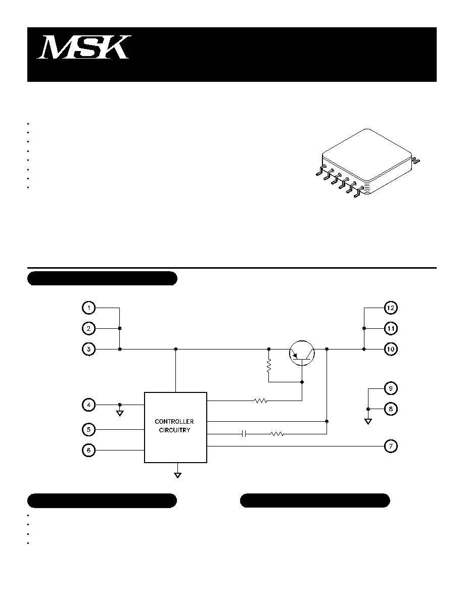
PIN-OUT INFORMATION
V
IN
A
V
IN
B
V
IN
C
GND 1
Latch
Shutdown
Total Dose Tested to 300K RAD
Ultra Low Dropout for Reduced Power Consumption
External Shutdown/Reset Function
Latching Overload Protection
Adjustable Output Using Two External Resistors
Output Current Limit
Surface Mount Package
Available to DSCC SMD # 5962-05220
1
2
3
4
5
6
Rev. F 2/06
1
V
OUT
A
V
OUT
B
V
OUT
C
GND 2
GND 2
FB
12
11
10
9
8
7
Input Voltage Range
Feedback Voltage
Feedback Pin Current
Quiescent Current
Line Regulation
Load Regulation
Dropout Voltage
Minimum Output Current
Output Voltage Range
Output Current Limit
Shutdown Threshold
Shutdown Hysteresis
Ripple Rejection
Phase Margin
Gain Margin
Equivalent Noise Voltage
Thermal Resistance
Storage Temperature Range
Lead Temperature Range
(10 Seconds)
Power Dissipation
Junction Temperature
ABSOLUTE MAXIMUM RATINGS
+10V
4A
-55∞C to +125∞C
-40∞C to +85∞C
Supply Voltage
Output Current
Case Operating Temperature Range
MSK5900RH K/H/E
MSK5900RH
-65∞C to +150∞C
300∞C
See SOA Curve
150∞C
1
2
3
4
5
6
7
8
9
10
T
ST
T
LD
P
D
T
C
+V
IN
I
OUT
T
C
Unless otherwise specified, V
IN
=5.0V, R1=1.62K, V
SHUTDOWN
=0V and I
OUT
=10mA. See Figure 2.
Guaranteed by design but not tested. Typical parameters are representative of actual device performance but are for reference only.
Industrial grade and "E" suffix devices shall be tested to subgroups 1 and 4 unless otherwise requested.
Military grade devices ("H" suffix) shall be 100% tested to subgroups 1,2,3 and 4.
Subgroup 5 and 6 testing available upon request.
Subgroup 1,4 T
C
=+25∞C
Subgroup 2,5 T
C
=+125∞C
Subgroup 3,6 T
A
=-55∞C
Output current limit is dependent upon the values of V
IN
and V
OUT
. See Figure 1 and typical performance curves.
Minimum V
IN
at -55∞C and I
OUT
=1.0A is 4.0V due to current limit circuitry.
Consult factory for post radiation limits.
Continuous operation at or above absolute maximum ratings may adversely effect the device performance and/or life cycle.
NOTES:
Group A
Subgroup
1
2,3
1
2,3
1,2,3
1
2,3
1
2,3
1
2,3
1
2,3
1
2,3
-
1
2,3
1
2,3
1
2,3
4
5,6
4,5,6
4,5,6
4,5,6
-
10mA
I
OUT
1.0A
10mA
I
OUT
1.0A R1=187
V
FB
=1.265V 10mA
I
OUT
1.0A
V
IN
=7.5V
Not Including I
OUT
I
OUT
=10mA 2.8V
V
IN
7.5V
R1=187
10mA
I
OUT
1.0A
Delta FB=1% I
OUT
=1.0A
2.8V
V
IN
7.5V
R1=187
V
IN
=7.5V
V
IN
=4.4V V
OUT
=3.3V
V
OUT
0.2V (OFF)
V
OUT
=Nominal (ON)
Difference between voltage
threshold of V
SDI
(ON) and V
SDI
(OFF)
f=1KHz to 10KHz
10mA
I
OUT
1.0A 1.0V=V
IN
-V
OUT
Referred to Feedback Pin
Junction to Case @ 125∞C Output Device
Typ.
-
-
1.265
-
-
14
14
±0.01
-
±0.06
-
0.22
0.26
8
9
-
1.75
1.75
1.3
1.3
0.02
0.03
-
-
70
18
-
6.9
Test Conditions
Max.
7.5
7.5
1.305
1.305
5.0
20
20
±0.50
±0.50
±0.80
±0.80
0.70
0.70
10
10
6.8
2.0
2.2
1.6
1.6
0.2
0.2
-
-
-
-
50
7.5
Min.
2.8
2.8
1.225
1.225
0
-
-
-
-
-
-
-
-
-
-
1.5
1.5
1.3
1.0
1.0
-
-
20
20
30
10
-
-
Min.
2.8
-
1.202
-
0
-
-
-
-
-
-
-
-
-
-
1.5
1.3
-
1.0
-
-
-
20
-
30
10
-
-
Max.
7.5
-
1.328
-
5.0
20
-
±0.60
-
±1.0
-
0.75
-
10
-
6.7
2.2
-
1.6
-
0.2
-
-
-
-
-
50
7.8
Typ.
-
-
1.265
-
-
14
-
0.01
-
0.06
-
0.22
-
8
-
-
1.75
-
1.3
-
0.02
-
-
-
70
18
-
6.9
V
V
V
V
µA
mA
mA
%V
OUT
%V
OUT
%V
OUT
%V
OUT
V
V
mA
mA
V
A
A
V
V
V
V
dB
dB
degrees
dB
µV
RMS
∞C/W
MSK5900K/H/E
MSK5900
Parameter
ELECTRICAL SPECIFICATIONS
2
Rev. F 2/06
Units
1
8
2
2
2
7
2
2
2
2
2
2
9
7
10
APPLICATION NOTES
PIN FUNCTIONS
V
IN
A,B,C - These pins provide power to all internal
circuitry including bias, start-up, thermal limit and
overcurrent latch. Input voltage range is 2.8V to 7.5V.
All three pins must be connected for proper operation.
GND1 - Internally connected to input ground, these pins
should be connected externally by the user to the circuit
ground and the GND2 pins.
LATCH - The MSK 5900RH has a timed latch-off circuit
which provides overcurrent protection. An overcurrent
or output short condition will saturate the internal drive
transistor. The time-out latch will then be triggered and
turn off the regulator. The time-out period is determined
by an external capacitor connected between the latch
and GND pins. Once the overcurrent condition is removed,
the latch can be reset by pulling the SHUTDOWN pin
high, grounding the LATCH pin or cycling power off,
then on. Under normal conditions, the voltage at the
LATCH pin is zero. When the device is latched off, the
voltage at the LATCH pin will be 1.6V at 25∞C.
SHUTDOWN - There are two functions to the SHUT-
DOWN pin. It may be used to disable the output voltage
or to reset the LATCH pin. To activate the shutdown/
reset functions the user must apply a voltage greater
than 1.3V to the SHUTDOWN pin. The output voltage
will turn on when the SHUTDOWN pin is pulled below
the threshold voltage. If the SHUTDOWN pin is not used,
it should be connected to ground.
FB - The FB pin is the inverting input of the internal error
amplifier. The non-inverting input is connected to an in-
ternal 1.265V reference. This error amplifier controls the
drive to the output transistor to force the FB pin to
1.265V. An external resistor divider is connected to the
output, FB pin and ground to set the output voltage.
GND2 - Internally connected to output ground, these pins
should be connected externally by the user to the circuit
ground and the GND1 pins.
V
OUT
A,B,C - These are the output pins for the device.
All three pins must be connected for proper operation.
To maximize transient response and minimize power
supply transients it is recommended that a 33µF
minimum tantalum capacitor is connected between V
IN
and ground. A 0.1µF ceramic capacitor should also be
used for high frequency bypassing.
OUTPUT CAPACITOR SELECTION
Typically, large bulk capacitance is required at the
output of a linear regulator to maintain good load tran-
sient response. However, with the MSK 5900RH this is
not the case. A 47µF surface mount tantalum capacitor
in parallel with a 0.1µF ceramic capacitor from the out-
put to ground should suffice under most conditions. If
the user finds that tighter voltage regulation is needed
during output transients, more capacitance may be added.
If more capacitance is added to the output, the band-
width may suffer.
OVERCURRENT LATCH-OFF/LATCH PIN
CAPACITOR SELECTION
As previously mentioned, the LATCH pin provides over
current/output short circuit protection with a timed latch-
off circuit. The latch off time out is determined with an
external capacitor connected from the LATCH pin to
ground. The time-out period is equal to the time it takes
to charge this external capacitor from 0V to 1.6V. The
latch charging current is provided by an internal current
source. This current is a function of input voltage and
temperature (see latch charging current curve). For in-
stance, at 25∞C, the latch charging current is 7.2µA at
V
IN
=3V and 8µA at V
IN
=7V.
In the latch-off mode, some additional current will be
drawn from the input. This additional latching current is
also a function of input voltage and temperature (see
latching current curve).
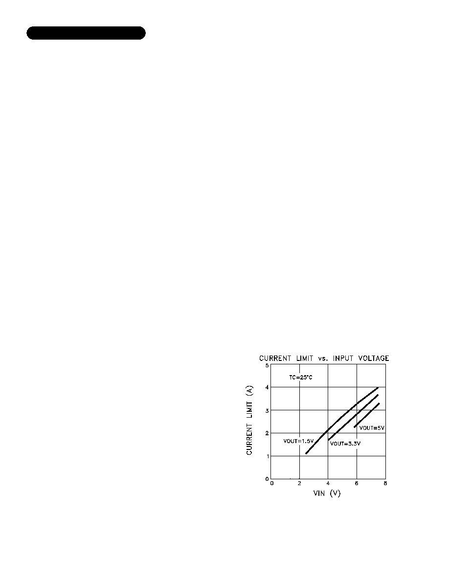
FIGURE 1
POWER SUPPLY BYPASSING
3
Rev. F 2/06
The MSK 5900RH current limit function is directly
affected by the input and output voltages. Figure 1
illustrates the relationship between V
IN
and I
CL
for three
output voltages.
APPLICATION NOTES CONT.
4
Rev. F 2/06
HEAT SINK SELECTION
To select a heat sink for the MSK 5900RH, the follow-
ing formula for convective heat flow may be used.
Governing Equation:
T
J
=
P
D
X (R
JC
+ R
CS
+ R
SA
) + T
A
Where
T
J
= Junction Temperature
P
D
= Total Power Dissipation
R
JC
= Junction to Case Thermal Resistance
R
CS
= Case to Heat Sink Thermal Resistance
R
SA
= Heat Sink to Ambient Thermal Resistance
T
A
= Ambient Temperature
Power Dissipation=(V
IN
-V
OUT
) x I
OUT
Next, the user must select a maximum junction tem-
perature. The absolute maximum allowable junction tem-
perature is 150∞C. The equation may now be rearranged
to solve for the required heat sink to ambient thermal
resistance (R
SA
).
Example:
An MSK 5900RH is connected for V
IN
=+5V and
V
OUT
=+3.3V. I
OUT
is a continuous 1A DC level. The
ambient temperature is +25∞C. The maximum desired
junction temperature is +125∞C.
R
JC
=7.5∞C/W and R
CS
=0.15∞C/W for most thermal
greases
Power Dissipation=(5V-3.3V) x (1A)
=1.7Watts
Solve for R
SA:
125∞C - 25∞C
1.7W
= 51.2∞C/W
In this example, a heat sink with a thermal resistance
of no more than 51∞C/W must be used to maintain a
junction temperature of no more than 125∞C.
THERMAL LIMITING
The MSK 5900RH control circuitry has a thermal shut-
down temperature of approximately 150∞C. This ther-
mal shutdown can be used as a protection feature, but
for continuous operation, the junction temperature of the
pass transistor must be maintained below 150∞C. Proper
heat sink selection is essential to maintain these condi-
tions.
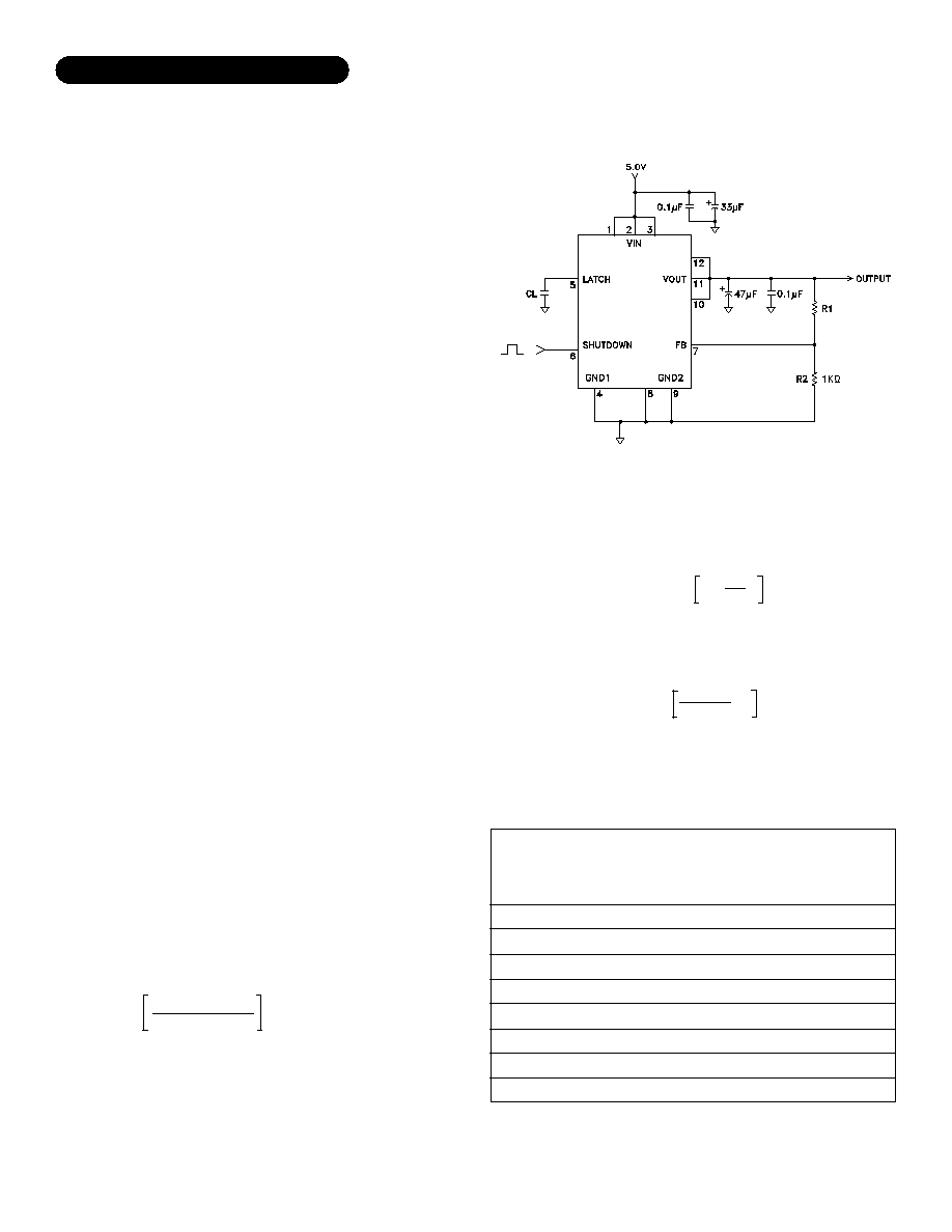
TYPICAL APPLICATIONS CIRCUIT
V
OUT
=1.265(1+R1/R2)
OUTPUT VOLTAGE SELECTION
As noted in the above typical applications circuit,
the formula for output voltage selection is
A good starting point for this output voltage selection is
to set R2=1K. By rearranging the formula it is simple to
calculate the final R1 value.
Table 1 below lists some of the most probable resistor
combinations based on industry standard usage.
TABLE 1
R1
R2
1+
V
OUT
=1.265
V
OUT
1.265
-1
R1=R2
1.5
1.8
2.0
2.5
2.8
3.3
4.0
5.0
R2
(
)
1K
1K
1K
1K
1K
1K
1K
1K
R1 (nearest 1%)
(
)
187
422
576
976
1.21K
1.62K
2.15K
2.94K
R
SA
= -7.5∞C/W - 0.15∞C/W
OUTPUT
VOLTAGE
(V)
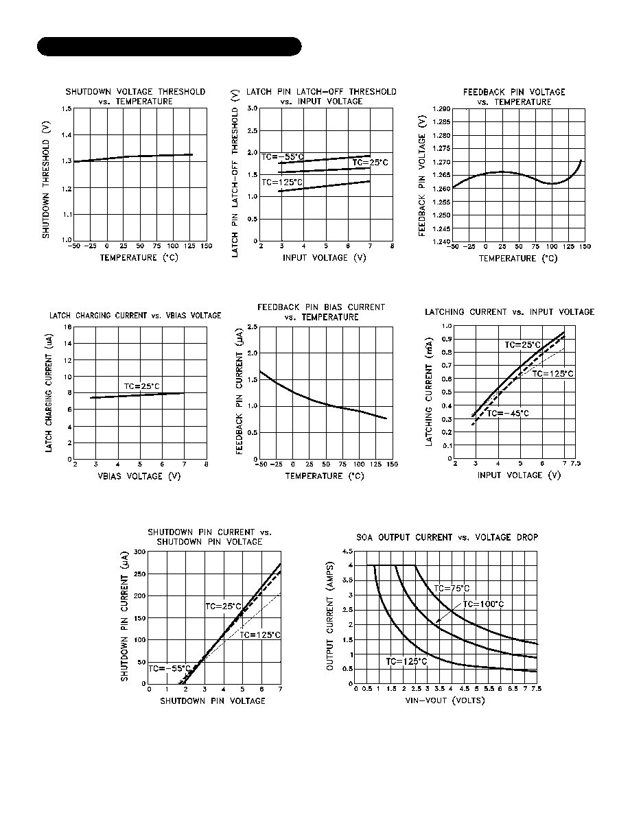
TYPICAL PERFORMANCE CURVES
Rev. F 2/06
5