4707 Dey Road Liverpool, N.Y. 13088
M.S.KENNEDY CORP.
(315) 701-6751
FEATURES:
Ultra Low Quiescent Current - ±15mA for High Voltage
150V Peak to Peak Output Voltage Swing
Slew Rate - 4200V/µS Typical
Gain Bandwidth Product - 550 MHz Typical
Full Power Output Frequency - 9 MHz Typical
Output Current - 250mA Peak
Adjustable VHV Power Supply Minimizes Power Dissipation
Compact Package Offers Superior Power Dissipation
WIDE BANDWIDTH
HIGH VOLTAGE AMPLIFIER
600
+VHV
+VSC
OUTPUT
CASE/GROUND
-VSC
-VHV
1
2
3
4
5
6
12
11
10
9
8
7
COMP
+VCC
GROUND
-VCC
-INPUT
NO CONNECTION
Wideband High Voltage Amplifier
High Resolution CRT Monitor
Ultra High Performance Video Processing
CRT Beam Intensity Control
Varactor Tuned VCO Driver
Automatic Test Equipment
PIN-OUT INFORMATION
TYPICAL APPLICATIONS
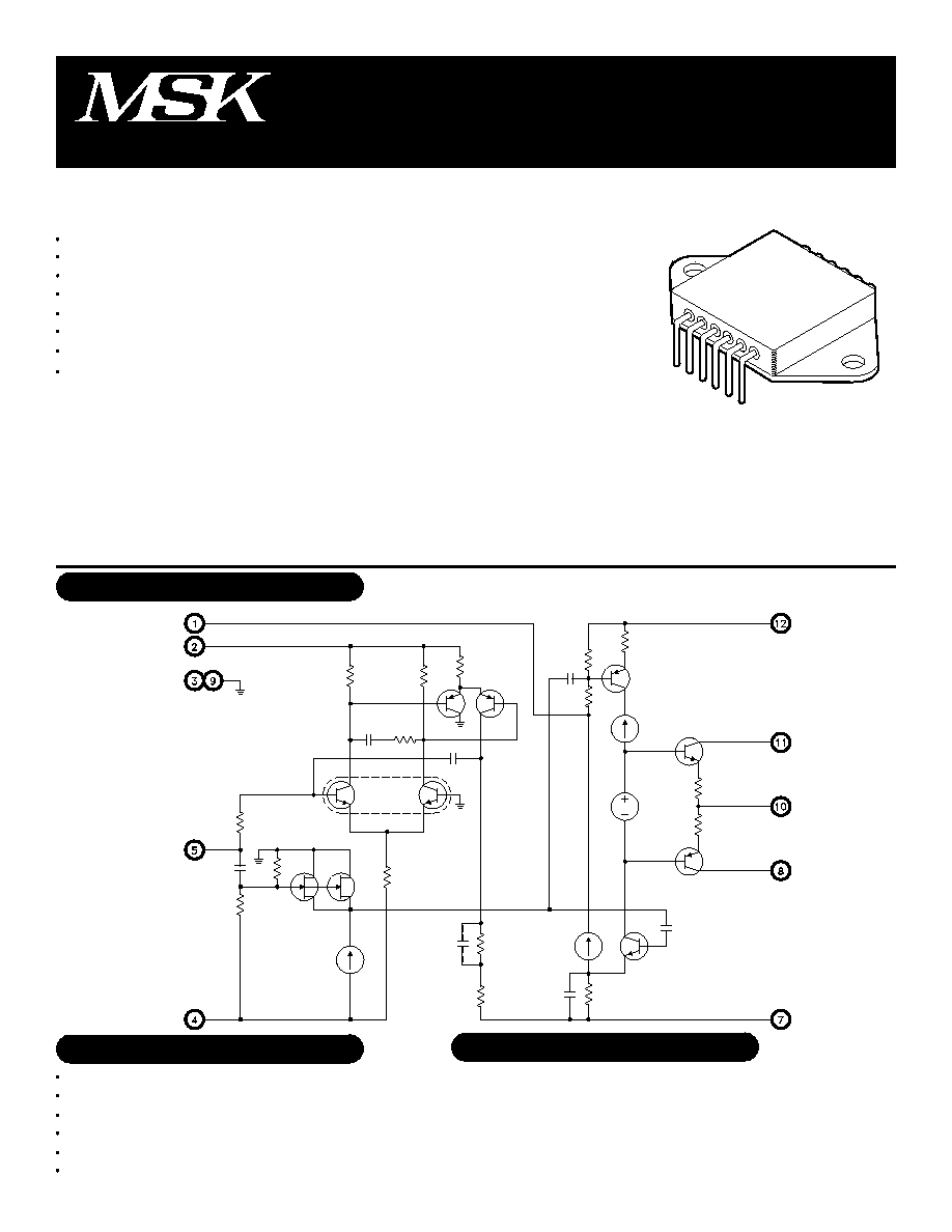
The MSK 600(B) is a high voltage wideband amplifier designed to provide large voltage swings at high slew rates
in wideband systems. The true inverting op-amp topology employed in the MSK 600 provides excellent D.C. specifi-
cations such as input offset voltage and input bias current. These attributes are important in amplifiers that will be
used in high gain configurations since the input error voltages will be multiplied by the system gain. The MSK 600
achieves impressive slew rate specifications by employing a feed forward A.C. path through the amplifier, however,
the device is internally configured in inverting mode to utilize this benefit. Internal compensation for gains of -5V/V or
greater keeps the MSK 600 stable in this range. The MSK 600 is packaged in a space efficient, hermetically sealed,
12 pin power dual in line package that has a high thermal conductivity for efficient device cooling.
DESCRIPTION:
EQUIVALENT SCHEMATIC
MIL-PRF-38534 QUALIFIED
ISO 9001 CERTIFIED BY DSCC
Rev. A 8/00
1
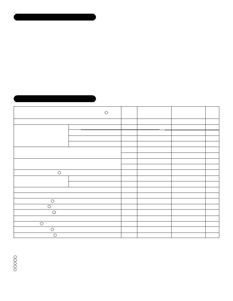
STATIC
Input Offset Voltage Drift
DYNAMIC CHARACTERISTICS
Output Voltage Swing
Peak Output Current
Full Power Output
Unity Gain Bandwidth
Slew Rate
Voltage Gain
Settling Time to 1%
Settling Time to 0.1%
Group A
Subgroup
1,2,3
1,2,3
1,2,3
1,2,3
1
2,3
1
2,3
2,3
-
-
4
-
-
-
4
4
-
-
±90V
DC
±V
CC
±18V
DC
30°C/W
-65°C to +150°C
300°C
-40°C to +85°C
-55°C to +125°C
150°C
ABSOLUTE MAXIMUM RATINGS
T
ST
T
LD
T
C
T
J
Storage Temperature Range
Lead Temperature Range
(10 Seconds)
Case Operating Temperature
MSK600
MSK600B
Junction Temperature
Supply Voltage
Input Voltage Range
Supply Voltage (Input Stage)
Thermal Resistance
(Output Devices)
±V
HV
±V
IN
±V
CC
JC
Typ.
1.0
12
15
15
±1.0
±2.0
50
100
±10
±15
±80
±72
±250
9
100
4200
100
200
500
Min.
-
-
-
-
-
-
-
-
-
±12
±50
±70
±200
2
80
3000
94
-
-
Max.
1.5
17
25
25
±5.0
±10.0
250
300
±50
±18
±90
-
-
-
-
-
-
-
-
Min.
-
-
-
-
-
-
-
-
-
±12
±50
±70
±200
1
80
2500
90
-
-
Max.
2.0
20
28
28
±10
-
500
-
-
±18
±90
-
-
-
-
-
-
-
-
MSK 600B
MSK 600
Parameter
Test Conditions
ELECTRICAL SPECIFICATIONS
1
mA
mA
mA
mA
mV
mV
nA
nA
µV/°C
V
V
V
mA
MHz
MHz
V/µS
dB
nS
nS
Units
Typ.
1.0
15
15
15
±1.0
±2.0
50
100
±10
±15
±80
±72
±250
9
100
4200
100
200
500
1
2
3
4
5
Unless otherwise specified, ±V
CC
=±15V
DC
, ±V
HV
=±80V
DC
, C
L
=8pF (probe capacitance) and A
V
=10V/V.
This parameter is guaranteed by design but not tested. Typical parameters are representative of actual device performance but are for reference only.
Industrial grade devices shall be tested to subgroups 1 and 4 unless otherwise specified.
Military grade devices ('B' suffix) shall be 100% tested to subgroups 1,2,3 and 4.
Subgroup 1,4 T
A
=T
C
=+25°C
Subgroup 2,5 T
A
=T
C
=+125°C
Subgroup 3,6 T
A
=T
C
=-55°C
NOTES:
Quiescent Current
Input Offset Voltage
Input Bias Current
V
IN
=0
V
IN
=0 @ +V
CC
V
IN
=0 @ -V
CC
V
IN
=0 @ +V
HV
V
IN
=0 @ -V
HV
V
IN
=0
±V
CC
±V
HV
f=1KHz
f=1KHz
V
0
=±70V
V
0
=±1.0V
V
0
=±70V
f=1KHz
A
V
=-10V/V V
O
=±60V
A
V
=-10V/V V
O
=±60V
Power Supply Range
2
2
2
2
2
2
2
Rev. A 8/00
2
APPLICATION NOTES
The MSK 600 employs a circuit topology known as "feed
forward". This inverting configuration allows the user to real-
ize the excellent D.C. input characteristics of a differential am-
plifier without losing system bandwidth. The incoming signal
is split at the input into its A.C. and D.C. component. The D.C.
component is allowed to run through the differential amplifier
where any common mode noise is rejected. The A.C. compo-
nent is "fed forward" to the output section through a very high
speed linear amplifier where it is mixed back together with the
D.C. component. The result is an amplifier with most of the
benefits of a differential amplifier without the loss in system
bandwidth.
FEED FORWARD TOPOLOGY
Transition time optimization of the MSK 600 follows the same
basic rules as most any other amplifier. Best transition times
will be realized with minumum load capacitance, minimum ex-
ternal feedback resistance and lowest circuit gain. Transition
times will degrade if the output is driven too close to either
supply rail. Feedback and input resistor values will affect tran-
sition time as well. See Figure 1 and Table 1 for recommended
component values.
Figure 1
CURRENT LIMIT
Figure 2 is the recommended active short circuit protection
scheme for the MSK 600. The following formula may be used
for setting current limit:
Current Limit
0.6V / Rsc
R
BASE
must be selected based on the value of ±V
HV
as fol-
lows:
R
BASE
= ((+V
HV
- (-V
HV
)) - 1.2V) / 4mA
This formula guarantees that Q2 and Q4 will always have suf-
ficient base current to be in operation. This circuit can be made
tolerant of high frequency output current spikes with the addi-
tion of C
SC
. The corresponding time constant would be:
T = (R
SC
) (C
SC
)
A common value for C
SC
is approximately 1000pF. If current
limit is unnecessary, short pin 7 to pin 8 and pin 11 to pin 12 as
shown in Figure 1.
1K
249
100
-R
IN
-10V/V
-20V/V
-50V/V
C
F
0.5-5pF
N/A
N/A
10K
5K
5K
VOLTAGE
GAIN
R
F
Table 1
Figure 2
INTERNAL COMPENSATION
Since the MSK 600 is a high voltage amplifier, it is com-
monly used in circuits employing large gains. Therefore, the
internal compensation was chosen for gains of -5V/V or greater.
In circuits running at gains of less than -5V/V, the user can
further compensate the device by adding compensation net-
works at the input or feedback node. Pin 1 (comp) should be
bypassed with a 0.1uF ceramic capacitor to +V
HV
for all appli-
cations.
HIGH VOLTAGE SUPPLIES
The positive and negative high voltage supplies on the MSK
600 can be adjusted to reduce power dissipation. The output
of the MSK 600 will typically swing to within 8V of either high
voltage power supply rail. Therefore, if the system in question
only needs the output of the amplifier to swing ±40V peak,
the power supply rails could be set to ±50V safely. For best
performance, the minimum value of ±V
HV
should be ±50V
DC
.
Unbalanced power supply rails are also allowed as long as one
or the other is not decreased to below 30V or above 90V. The
high voltage and low voltage power supplies should be decoupled
as shown in Figure 1.
TRANSITION TIMES
Rev. A 8/00
3

