The MSK 645 is an amplifier designed specifically to suit the needs of todays high resolution CRT display moni-
tors. With a typical bandwidth of 150 MHz and transition times typically under 3.0nS the MSK 645 can easily drive
monitors with resolutions of up to 1280 x 1024. The output can swing up to 65 Vpp and gain is internally set to minimize
external component count. The MSK 645(B) is available screened to MIL-PRF-38534 and comes in a space efficient pack-
age that is electrically isolated from the internal circuitry and can be attached directly to a heat sink for efficient thermal
dissipation.
FEATURES:
4707 Dey Road Liverpool, N.Y. 13088
M.S.KENNEDY CORP.
(315) 701-6751
HIGH PERFORMANCE,
HIGH VOLTAGE
VIDEO DISPLAY DRIVER
645
ISO-9001 CERTIFIED BY DSCC
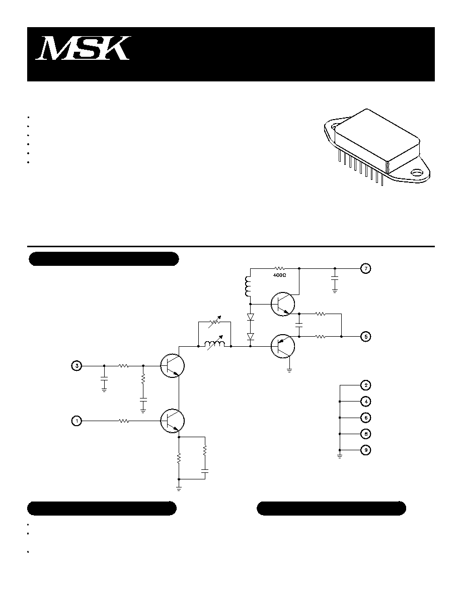
EQUIVALENT SCHEMATIC
65 Vpp Output Voltage
150 MHz Typical Bandwidth
Transition Times Typically <3.0 nS
Cost and Space Efficient Package
Electrically Isolated Case
Gain Fixed Internally
DESCRIPTION:
MIL-PRF-38534 CERTIFIED
CRT Driver for SVGA
Display Driver for Systems with up to
1280 x 1024 Display Resolution
High Voltage Fixed Gain Amplifier
PIN-OUT INFORMATION
1
2
3
4
5
6
7
8
9
TYPICAL APPLICATIONS
Video Input
Ground
V
BIAS
Ground
Video Output
Ground
+V
HV
Ground
Ground
Rev. D 10/05
1
2.0
0.5
80
10
1.3
-
10
80
±3.0
5.0
12
-
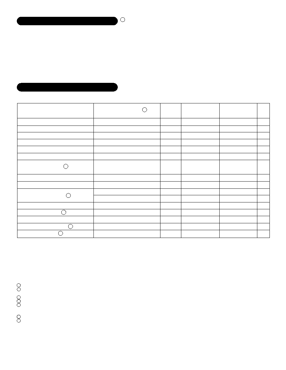
STATIC CHARACTERISTICS
Quiescent Current (V
HV
)
Quiescent Current (+V
BIAS
)
V
HV
Power Supply Range
V
BIAS
Power Supply Range
Video Input Voltage
DYNAMIC CHARACTERISTICS
Video Gain
Video Gain Flatness 2
Video Output Rise/Fall Time
Video Output Overshoot 2
Bandwidth -3dB 2
mA
mA
V
V
V
V
V
V/V
dB
nS
%
MHz
Storage Temperature Range
Lead Temperature Range
(Solder 10 Seconds)
Junction Temperature
Case Operating Temperature
MSK645
MSK645(B)
+V
HV
+V
IN
+V
BIAS
I
OUT
High Voltage Supply
Input Voltage
Bias Input Voltage
Peak Output Current
+80V
±5V
+10V
200mA
T
ST
T
LD
T
J
T
C
ABSOLUTE MAXIMUM RATINGS
-65∞C to +150∞C
+300∞C
+175∞C
-40∞C to +85∞C
-55∞C to +125∞C
ELECTRICAL SPECIFICATIONS
Min. Typ. Max.
V
IN
=No Connect R
L
=
V
IN
=No Connect R
L
=
V
OUT
=+50VDC
Output Stage
Junction to Case @ 125∞C
High Level
Low Level
F=1MHz;V
OUT
=+15Vto+45V
F=10Hz to 60MHz;V
OUT
=30V
PP
V
OUT
=+15Vto+45V
V
OUT
=10V
PP
V
IN
T
R
=10nS
-
-
20
4
0.4
50
-
45
-
-
-
100
0.6
0.01
60
5
0.85
59
5
60
±1.0
3.0
-
150
-
-
20
4
0.5
50
-
45
-
-
-
100
0.6
0.01
60
5
0.85
59
5
62
±1.0
3.0
-
150
1,2,3
1,2,3
-
-
1,2,3
4
4
4
-
4
-
4
Min. Typ. Max.
MSK 645(B) MSK 645
Video Output Voltage
2.0
0.5
80
10
1.2
-
10
80
±2.0
4.0
10
-
1
2
3
4
5
6
7
NOTES:
+V
HV
=60V; +V
BIAS
=5V; R
L
=10K
; unless otherwise specified.
Parameter is guaranteed by design but not tested. Typical specifications are representative of actual device
performance at 25∞C but are for reference only.
Military grade devices ('B' suffix) shall be 100% tested to subgroups 1,2,3 and 4.
Subgroup 5 and 6 testing available upon request.
Subgroup 1,4 T
A
=T
C
=+25∞C
Subgroup 2,5 T
A
=T
C
=+125∞C
Subgroup 3,6 T
A
=T
C
=-55∞C
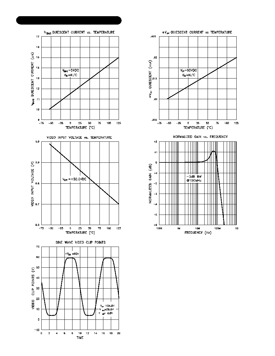
Refer to the video clip point curve on the Typical Performance Curves page.
Continuous operation at or above absolute maximum ratings may adversely effect the device performance
and/or life cycle.
6
Parameter
Test Conditions
Group A
Subgroup
1
Units
Rev. D 10/05
2
Thermal Resistance 2
-
-
26
30
26
32
-
∞C/W
7

APPLICATION NOTES
BLACK LEVEL CONTROL
Unlike many currently available video amplifiers, the MSK 645
is a D.C. coupled device. D.C. coupling affords the user direct
black level control. A video input voltage of approximately
0.85 volts will set the output voltage to 50VDC (black level for
+V
HV
=60VDC). Black level control grants the user flexibility
in the application of the amplifier. For example, the user could
apply a 0.85VDC level to the video input to bias the output at
the black level (approximately 50V for V
HV
=60V) and have
input video information swing from 0.85 to 1.5V causing the
output to swing from the black level towards white (zero).
This configuration would dissipate the least amount of power
and is most common. Another possible circuit configuration
could be to D.C. bias the video input pin so that the output is
at 1/2V
HV
. The output video signal could then swing linearly
from (+V
HV
-10V) to (ground + 10V). Careful consideration
must be paid to device power dissipation in this configuration
since it will be very high.
VBIAS INPUT
The V
BIAS
pin is connected to the base of the cascode tran-
sistor in the equivalent schematic. The purpose of the cascode
transistor is to isolate the input transistor from the high volt-
age supply. The input transistor must have a very high transi-
tion frequency specification and this is difficult to find in high
voltage transistors. By using the cascode transistor to relieve
the input transistor of its high BVceo requirement, high speed,
low breakdown transistors can be used. The voltage applied
to pin three minus a base to emitter voltage drop of approxi-
mately 0.6 volts is the voltage present at the collector of the
input transistor that acts as the voltage to current convertor.
The voltage applied to the V
BIAS
pin has a practical upper limit
of 10.0 volts. Above 10.0 volts the device may not be able to
reach white level without going into cutoff. The practical lower
limit for this pin is approximately 2.0 volts. Below 2.0 volts
the input transistor will be dangerously close to cutoff. The
MSK 645 functions best with V
BIAS
set to 5.0 volts ±1.0 volt.
OUTPUT CONSIDERATIONS
The output of the MSK 645 is driven by a complimentary
push-pull buffer. The output stage isolates the capacitive load
from the amplifier thereby making rising and falling edges rela-
tively load independent. The bandwidth of the MSK 645 is
limited by the RC time constant made up of the resistance
from +V
HV
to the base of the NPN buffer and the capacitance
from the NPN buffer base to ground. The coils in the equiva-
lent schematic are chosen at the factory to moderately peak
the amplifiers response (10%). For application specific user
adjustable peaking, see the Typical Connection Circuit page.
OUTPUT PROTECTION
High voltage arcing can occur in the CRT being driven and
cause severe damage to the MSK 645 output unless certain
precautions are taken. The clamp diodes D1 and D2 (see fig-
ure 1) will keep the voltage at the output at a safe level. These
diodes should have a low series resistance and shunt capaci-
tance as well as a high surge rating (FDH400 is recommended).
In the event of an arcover, Rb limits the current flowing through
the clamp diode and Ra limits the current into the MSK 645
output. The recommended values shown in figure 1 should
not be deviated from without checking the monitor performance
since increasing these values will adversely affect transistion
times.
HEAT SINK SELECTION
To calculate what size heat sink is needed for a particular ap-
plication, the following formula must be used:
Tj = Pd (R
jc + R
sa) + Ta
where:
Tj=junction temperature = 150∞C max.
R
jc=30∞C/W max.
Ta is the ambient temperature and Pd is the device power dis-
sipation. R
sa is the heat sink thermal resistance.
EXAMPLE:
In an application an MSK 645 is dissipating 4 watts of power
and the ambient temperature is +25∞C. Plugging in all the
known variables and rearranging the equation it can be seen
that:
R
sa = ((150∞C - 25∞C)/4W) - 30∞C/W
= 1.2∞C/W
A heat sink with a thermal resistance of no more than 1.2∞C/W
must be used to maintain a junction temperature of 150∞C max.
POWER DISSIPATION
The most efficient method to reduce device power dissipa-
tion when using the MSK 645 is to fix the black level at a point
as close to +V
HV
as possible and maintain the peak to peak
video output voltage to as small an excursion as possible. The
case of the MSK 645 is electrically isolated from internal cir-
cuitry and therefore the user should attach the heat sink di-
rectly to the case of the device.
POWER SUPPLY DECOUPLING
Both the +V
HV
and the V
BIAS
input pins are decoupled inter-
nally with 0.1µF capacitors to contain line noise. However it is
good practice to decouple the MSK 645 externally with at least
a 4.7µF electrolytic capacitor placed as close as possible to
the associated device pins.
Rev. D 10/05
3