 | ÐлекÑÑоннÑй компоненÑ: MSK738 | СкаÑаÑÑ:  PDF PDF  ZIP ZIP |
Äîêóìåíòàöèÿ è îïèñàíèÿ www.docs.chipfind.ru
4707 Dey Road Liverpool, N.Y. 13088
M.S.KENNEDY CORP.
(315) 701-6751
FEATURES:
738
ISO-9001 CERTIFIED BY DSCC
INVERTING
Very Fast Settling Time
Very Fast Slew Rate
Wide Bandwidth
Low Noise
Very Accurate (Low Offset)
MIL-PRF-38534 CERTIFIED
DESCRIPTION:
The MSK 738 is an inverting operational amplifier that exhibits an impressive combination of high speed and precision
D.C. characteristics. The Op-amp's very fast slew rate, very fast settling time and wide bandwidth, along with its ex-
tremely low input offset voltage, offset drift and low noise, make it an outstanding performer.
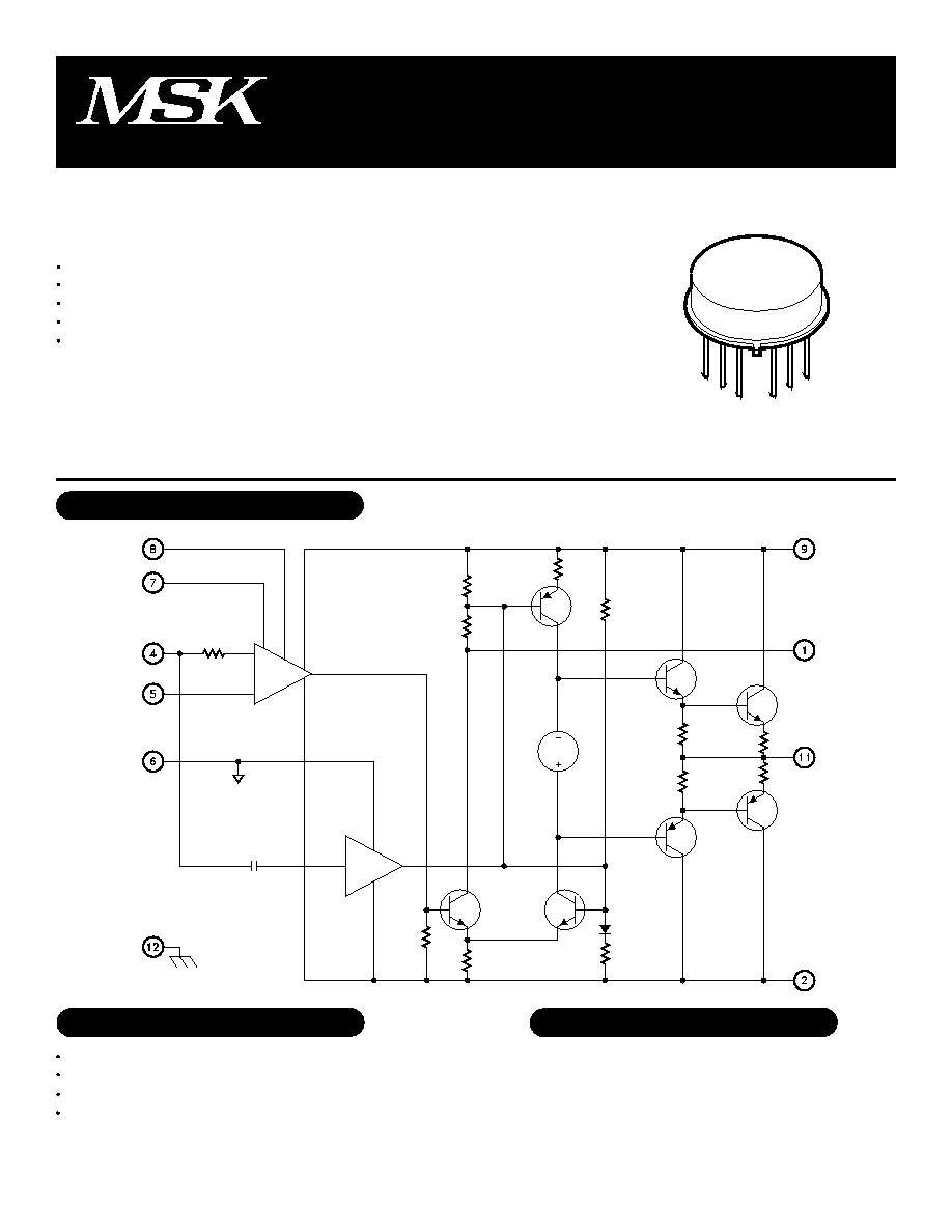
EQUIVALENT SCHEMATIC
TYPICAL APPLICATIONS
TYPICAL APPLICATIONS
PIN-OUT INFORMATION
High Performance Data Aquisition
Coaxial Line Driver
Data Conversion Circuits
High Speed Communications
Compensation
Negative Power Supply
NC
Inverting Input
Non-Inverting Input
Ground
1
2
3
4
5
6
Balance
Balance
Positive Power Supply
NC
Output
Case Connection
7
8
9
10
11
12
Rev. B 6/03
1
EQUIVALENT SCHEMATIC
OPERATIONAL AMPLIFIER
STATIC
Supply Voltage Range
Quiescent Current
Thermal Resistance
INPUT
Input Offset Voltage
Input Offset Voltage Drift
Input Offset Adjust
Input Bias Current
Input Offset Current
Input Impedance
Power Supply Rejection Ratio
Input Noise Voltage
Input Noise Voltage Density
Input Noise Current Density
OUTPUT
Output Voltage Swing
Output Current
Settling Time
1
Full Power Bandwidth
Bandwidth (Small Signal)
TRANSFER CHARACTERISTICS
Supply Voltage
Peak Output Current
Differential Input Voltage
Case Operating Temperature Range
(MSK 738B/E) -55°C to+125°C
(MSK 738) -40°C to +85°C
Storage Temperature Range -65°C to +150°C
Lead Temperature Range
300°C
(10 Seconds Soldering)
Power Dissipation See Curve
Junction Temperature 150°C
Group A
Subgroup
-
1
2,3
-
1
2,3
1
2,3
1
2,3
1
2,3
-
-
-
-
-
4
4
4
4
4
4
4
V
mA
mA
°C/W
µV
µV/°C
m V
m V
nA
nA
nA
nA
M
µV/V
µVp-p
nV
Hz
pA
Hz
V
mA
nS
MHz
MHz
V/µS
V
IN
=0V
A
V
=-1V/V
Junction to Case Output Devices
Bal. Pins=NC V
IN
=0V A
V
=-100V/V
V
IN
=0V
R
POT
=10K
To+V
CC
A
V
=-1V/V
V
CM
=0V
Either Input
V
CM
=0V
F=DC Differential
V
CC
=±5V
F= 0.1Hz To 10Hz
F=1KHz
F=1KHz
R
L
=100
A
V
=-3V/V F
20MHz
A
V
=-3V/V T
J
<150°C
0.1% 10V step
R
L
=100
Vo=±10V
R
L
=100
V
OUT
=±10V R
L
=100
Av=-1.5V/V
+18V
±200mA
±12V
±V
CC
I
OUT
V
IN
T
C
Parameter
T
ST
T
LD
P
D
T
J
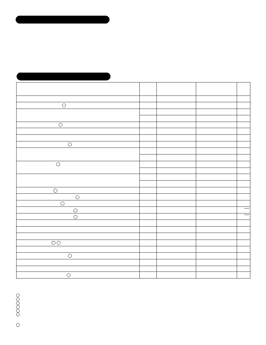
ELECTRICAL SPECIFICATIONS
ABSOLUTE MAXIMUM RATINGS
Test Conditions
NOTES:
AV= -1, measured in false summing junction circuit.
Guaranteed by design but not tested. Typical parameters are representative of actual device performance but are for reference only.
Industrial grade and "E" suffix devices shall be tested to subgroups 1 and 4 unless otherwise specified.
Military grade devices ("B" suffix) shall be 100% tested to subgroups 1,2,3 and 4.
Subgroups 5 and 6 testing available upon request.
Subgroup 1,4
Subgroup 2,5
Subgroup 3,6
Measurement taken 0.5 seconds after application of power using automatic test equipment.
T
A
=T
C
=+25°C
T
A
=T
C
=+125°C
T
A
=T
C
=-55°C
MSK 738B/E
Min.
±12
-
-
-
-
-
-
-
-
-
-
-
-
-
-
±10
±100
-
20
175
Typ.
±15
±39
±40
46
±25
±0.5
±10
±20
2
5
5
1
0.15
3.8
0.6
±12
±120
30
22
200
3500
Max.
±18
±40
±42
-
±75
±1
±40
±80
20
40
-
10
-
-
-
-
-
40
-
-
-
Typ.
±15
±39
-
46
±50
-
-
±20
-
10
-
5
2
0.2
4
0.7
±11.8
±120
35
20
190
MSK 738
Min.
±12
-
-
-
-
-
-
-
-
-
-
-
-
-
-
-
±10
±100
-
15
165
3500
Max.
±18
±42
-
-
±100
-
-
±60
-
30
-
-
20
-
-
-
-
-
45
-
-
-
Units
Rev. B 6/03
2
Slew Rate
3200
3200
100
110
-
95
105
-
dB
2
2
±Vcc=±15V Unless Otherwise Specified
1
5
7
3
4
2
6
Adjust to zero
Adjust to zero
2
2
2
2
2
7
2
Adjust to zero
2
2
2
Open Loop Voltage Gain R
L
=1K
F=1KHz
V
OUT
=±10V
APPLICATION NOTES
HEAT SINKING
To determine if a heat sink is necessary for your application and
if so, what type, refer to the thermal model and governing equation
below.
Governing Equation:
Example
:
This example demonstrates a worst case analysis for the op-amp
output stage. This occurs when the output voltage is 1/2 the power
supply voltage. Under this condition, maximum power transfer oc-
curs and the output is under maximum stress.
Conditions:
V
CC
=±16VDC
V
O
=±8Vp Sine Wave, Freq.=1KHz
R
L
=100
For a worst case analysis we will treat the +8Vp sine wave
as an 8VDC output voltage.
1.) Find Driver Power Dissipation
P
D
=(VCC-VO) (VO/RL)
=(16V-8V) (8V/100
)
=0.64W
2.) For conservative design, set T
J
=+125°C
3.) For this example, worst case T
A
=+90°C
4.) R
JC
=46°C/W from MSK 738B Data Sheet
5.) R
CS
=0.15°C/W for most thermal greases
6.) Rearrange governing equation to solve for R
SA
R
SA
=((
T
J
-
T
A
)/
P
D
) - (
R
JC
) - (
R
CS
)
=((125°C -90°C)/0.64W) - 45°C/W - 0.15°C/W
=54.7 - 46.15
=8.5°C/W
Rev. B 6/03
3
T
J
=
P
D
x
(R
JC +
R
CS
+
R
SA
)
+
T
A
Where
T
J=
Junction Temperature
P
D=
Total Power Dissipation
R
JC=
Junction to Case Thermal Resistance
R
CS=
Case to Heat Sink Thermal Resistance
R
SA=
Heat Sink to Ambient Thermal Resistance
T
C=
Case Temperature
T
A=
Ambient Temperature
T
S=
Sink Temperature
Potentiometer values ranging from 1K
to 1M
can be used with
only a small amount of degradation (typically 0.15 to 0.25µV/°C) of
input offset voltage drift. If the input offset voltage is to be trimmed
to a value other than "zero", the following formula can be used to
approximate the change in input offset voltage drift:
V
OSD
=V
OS
(trimmed)/250
Recommended External Component Selection Guide
APPROXIMATE
DESIRED GAIN
RI(+) RI(-) Rf(Ext) Cf
-1 499
1K
1K
-2 330
499
1K
-5 169
200
1K
-8 100
124
1K
90.9
100
1K
-20
-10
100
100
2K
1 The positive input resistor is selected to minimize any bias current induced offset
voltage.
2 The feedback capacitor will help compensate for stray input capacitance. The value of
this capacitor can be dependent on individual applications. A 2 to 9 pf capacitor is
usually optimum for most applications.
Thermal Model:
The heat sink in this example must have a thermal resistance of
no more than 8.5°C/W to maintain a junction temperature of no
more than +125°C.
OFFSET NULL
Typically, the MSK 738(B) has an input offset voltage of less than
±25µV. If it is desirable to adjust the offset closer to "zero", or to
a value other than "zero", the circuit below is recommended. R
P
should be a ten-turn 10K
potentiometer. Typical offset adjust is
±5mV.
2
2
2
2
2
2
1
1
1
1
1
1
1µf
1µf
1µf
1µf
1µf
1µf
C1
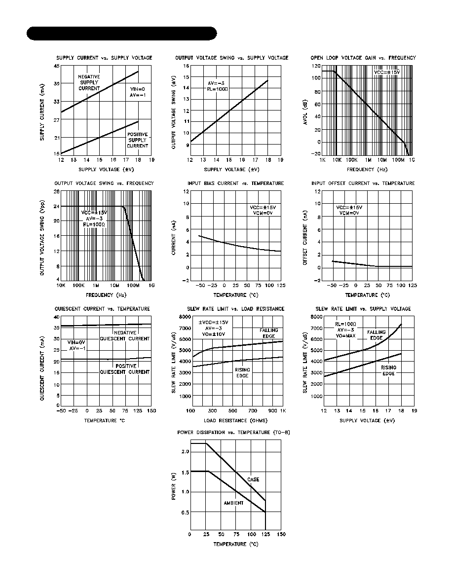
TYPICAL PERFORMANCE CURVES
Rev. B 6/03
4
The information contained herein is believed to be accurate at the time of printing. MSK reserves the right to make
changes to its products or specifications without notice, however, and assumes no liability for the use of its products.
Please visit our website for the most recent revision of this datasheet.
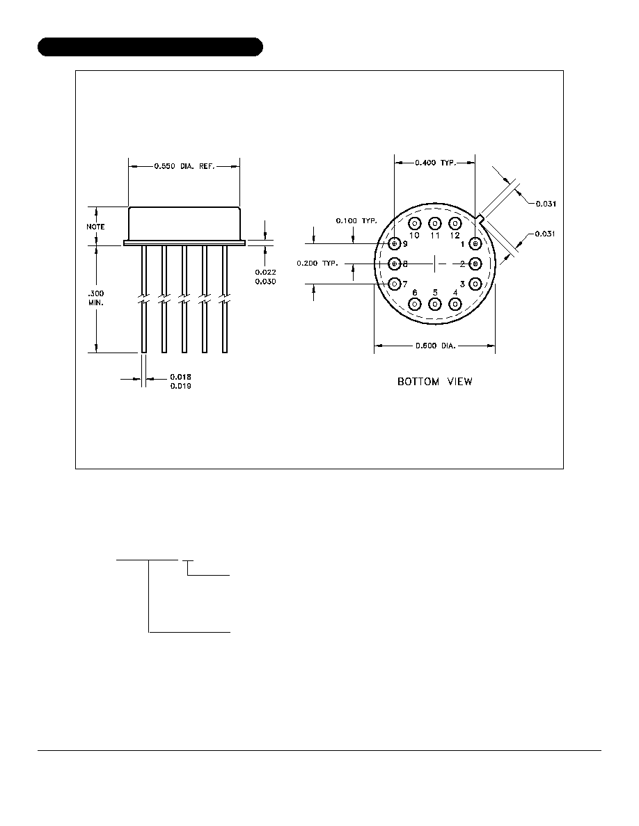
MECHANICAL SPECIFICATIONS
M.S. Kennedy Corp.
4707 Dey Road, Liverpool, New York 13088
Phone (315) 701-6751
FAX (315) 701-6752
www.mskennedy.com
NOTE: ALL DIMENSIONS ARE ±0.010 INCHES UNLESS OTHERWISE LABELED.
ORDERING INFORMATION
Rev. B 6/03
5
NOTE:Standard cover height:
MSK 738 0.200 Max.
Alternate lid heights available
MSK738 B
SCREENING
GENERAL PART NUMBER
BLANK=INDUSTRIAL; B=MIL-PRF-38534 CLASS H
E=EXTENDED RELIABILITY