Document Outline
- ˛ˇ
- ˛ˇ
- ˛ˇ
- ˛ˇ
- ˛ˇ
- ˛ˇ
- ˛ˇ
- ˛ˇ
- ˛ˇ
- ˛ˇ
- ˛ˇ
- ˛ˇ
- ˛ˇ
- ˛ˇ
- ˛ˇ
- ˛ˇ
- ˛ˇ
- ˛ˇ
- ˛ˇ
- ˛ˇ
- ˛ˇ
- ˛ˇ
- ˛ˇ

Murata
Manufacturing Co., Ltd.
Cat.No.P25E-3
CERAFILr(Filters/Traps/Discriminators) for TV/VCR
CERAFILr
(FILTERS/TRAPS
/DISCRIMINATORS)
FOR TV/VCR
Please read CAUTION and Notice in this catalog for safety. This catalog has only typical specifications. Therefore you are requested
to approve our product specification or to transact the approval sheet for product specification, before your ordering.
P25E3.pdf 01.10.17
1
2
3
4
5
6
7
8
9
10
11
12
13
14
Part Numbering
2
CERAFILr Chip Type SFSKA Series
4
CERAFILr Chip Type Notice
5
CERAFILr Picture Band Low-Suprious SFSRA Series
6
CERAFILr Low-profile SFSRL Series
11
CERAFILr High-selectivity Type SFTRD Series
14
CERAFILr Chroma Signal SFSRA/H/L Series
17
CERAFILr Lead Type Notice
19
Ceramic Traps Chip Type TPSKA Series
20
Double Trap Chip Type TPWKA Series
21
Ceramic Trap Chip Type Notice
22
Ceramic Traps Three-terminals TPSRA Series
23
Ceramic Traps Two-terminals TPSRD Series
26
Ceramic Traps TPSRD Series for 2ch Sound TV in Germany
29
Double Traps TPWRD Series
30
Triple Traps TPTRD Series
32
Ceramic Trap Lead Type Notice
33
Discriminators Wide-Band Type CDSRH Series
34
Discriminators Low-Profile Type CDSRL Series
36
Ceramic Discriminator Notice
38
Chip Type Packaging
39
Lead Type Packaging
40
CONTENTS
CERAFILr in this catalog are the trademarks of Murata Manufacturing Co., Ltd.
2
1
3
4
5
6
7
8
9
10
11
12
13
14
Please read CAUTION and Notice in this catalog for safety. This catalog has only typical specifications. Therefore you are requested
to approve our product specification or to transact the approval sheet for product specification, before your ordering.
P25E3.pdf 01.10.17

2
u
-B0
e
RA
w
S
r
4M50
y
00
t
CF
q
SF
(Global Part Number)
qProduct ID
wOscillation/Numbers of Element
CERAFIL
r
for TV/VCR
SF
Ceramic Filters
Product ID
tProduct Specification Code (1)
AF
BF
CF
DF
EF
Code
Product Specification Code (1)
Radial taping is applied to lead type and plastic taping to chip type.
With non-standard products, two-digit alphanumerics indicating
"Individual Specification" is added between "
tProduct Specification
Code (1)" and "
yProduct Specification Code (2)".
eStructure/Size
Bulk
Radial Taping H
0
=18mm
Plastic Taping ¯=330mm
Standard Bandwidth Type
Tight Bandwidth Type
Standard Bandwidth Type
Broad Bandwidth Type
Ultra-broad Bandwidth Type
yProduct Specification Code (2)
00
Code
Product Specification Code (2)
Standard Type
uPackaging
-B0
-A0
-R1
Code
Packaging
2 Elements Thickness Shear mode
3 Elements Thickness Expander mode
S
T
Code
Oscillation/Numbers of Element
Lead Type
Chip Type
R
p
K
p
Code
Structure/Size
p is expressed "
A
" or subsequent code, which indicates the size.
The code
AF
is only applied to
SFT
series.
rNominal Center Frequency
Expressed by four-digit alphanumerics. The unit is in hertz (MHz).
Decimal point is expressed by capital letter "M".
o
Part Numbering
The structure of the "Global Part Numbers" that have been adopted since June 2001 and the meaning of each code are described herein.
If you have any questions about details, inquire at your usual Murata sales office or distributor.
(
)
y
00
u
-B0
e
RA
w
S
r
4M50
t
B
q
TP
(Global Part Number)
qProduct ID
wFunction
Ceramic Traps
TP
Ceramic Traps
Product ID
tProduct Specification Code (1)
B
C
Code
Product Specification (1)
Radial taping is applied to lead type and plastic taping to chip type.
With non-standard products, three-digit alphanumerics indicating
"Individual Specification" is added between "
yProduct Specification
Code (2)" and "
uPackaging".
eStructure/Size
Bulk
Radial Taping H
0
=18mm
Plastic Taping ¯=330mm
Broad-bandwidth Type
Low-capacitance Type
yProduct Specification Code (2)
00
Code
Product Specification Code (2)
Standard Type
uPackaging
-B0
-A0
-R1
Code
Packaging
Single Traps
Triple Traps
Double Traps
S
T
W
Code
Function
Lead Type
Chip Type
R
p
K
p
Code
Structure/Size
p is expressed "
A
" or subsequent code, which indicates the size.
rNominal Center Frequency
Expressed by four-digit alphanumerics. The unit is in hertz (MHz).
Decimal point is expressed by capital letter "M".
Please read CAUTION and Notice in this catalog for safety. This catalog has only typical specifications. Therefore you are requested
to approve our product specification or to transact the approval sheet for product specification, before your ordering.
P25E3.pdf 01.10.17

3
e
RH
w
S
r
4M50
t
E
y
K
i
-A0
u
048
q
CD
(Global Part Number)
qProduct ID
wOscillation
Discriminators for TV/VCR
CD
Discriminators
Product ID
tProduct Specification Code (1)
C
E
Code
Product Specification Code (1)
With non-standard products, an alphabet Indicating "Individual
Specification" is added between "
uIC" and "iPackaging".
eStructure/Size
Bulk
Radial Taping H
0
=18mm
Three-terminals
Two-terminals
yProduct Specification Code (2)
K
Code
Product Specification Code (2)
Specification
uIC
048
Code
IC
Applicable IC control code
iPackaging
-B0
-A0
Code
Packaging
Thickness Shear mode
S
Code
Oscillation
Standard Type
Low-profile
RH
RL
Code
Structure/Size
rNominal Center Frequency
Expressed by four-digit alphanumerics. The unit is in hertz (MHz).
Decimal point is expressed by capital letter "M".
Please read CAUTION and Notice in this catalog for safety. This catalog has only typical specifications. Therefore you are requested
to approve our product specification or to transact the approval sheet for product specification, before your ordering.
P25E3.pdf 01.10.17

Please read CAUTION and Notice in this catalog for safety. This catalog has only typical specifications. Therefore you are requested
to approve our product specification or to transact the approval sheet for product specification, before your ordering.
P25E3.pdf 01.10.17
4
1
CERAFILr(Filters/Traps/Discriminators) for TV/VCR
CERAFIL
r
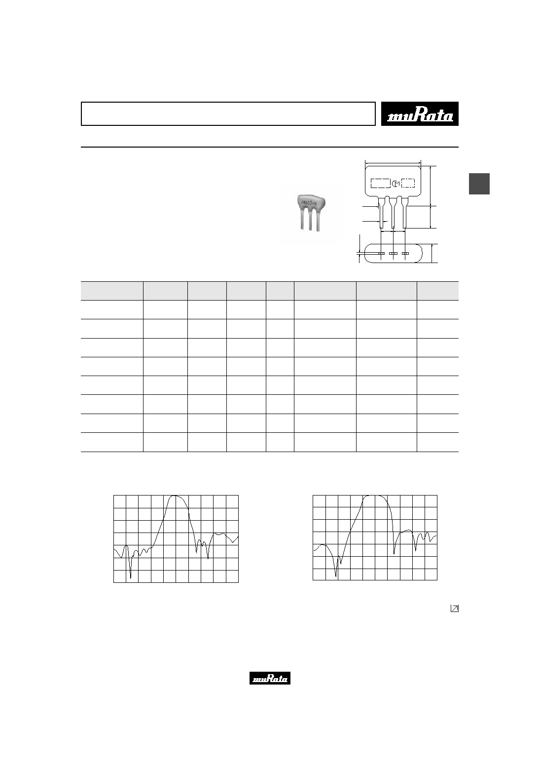
Chip Type SFSKA Series
SMD ceramic filter SFSKA_CF is a small and thin SMD
filter sealed with a metal cap.
Recommended for LCD-TVs, and small and thin tuners.
s Features
1. High attenuation outside bandwidth.
2. Small and thin pakage.
3. Reflow-solderable.
(1) : Input
(2) : Ground
(3) : Output
: Vender's Code
: EIAJ monthly Code
7.9
±
0.2
3.0
±
0.1
8.5
±
0.2
3.8
±
0.2
1.8
±
0.2
0.5
±
0.1
0.6
±
0.2
1.0
±
0.1
1.3
±
0.2
2.5
±
0.2 2.5
±
0.2
0.3
±
0.1
1.3
±
0.2
(1)
(2)
(3)
Electrode
in mm
Part Number
Nominal Center
Frequency (fn)
(MHz)
3dB
Bandwidth
(kHz)
20dB
Bandwidth
(kHz)
Insertion
Loss
(dB)
Spurious
Attenuation(1)
(dB)
Spurious
Attenuation(2)
(dB)
Input/Output
Impedance
(ohm)
SFSKA4M50CF00-R1
4.500
fn
±
60 min.
600 max.
6.0 max.
20 min.
[within 0 to fn]
15 min.
[within fn to 7.0MHz]
1000
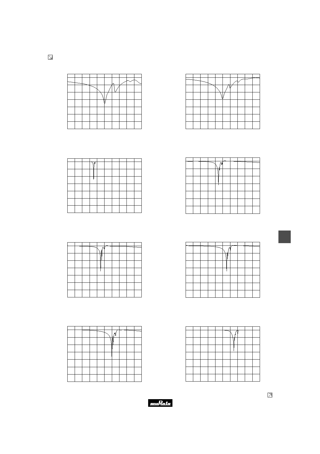
s Frequency Characteristics
3.5
3.9
3.7
4.1
4.5
4.9
5.3
4.3
Attenuation (dB)
4.7
Frequency (MHz)
5.1
5.5
0
10
20
30
40
50
60
70
s Spurious Response
0.0
2.0
4.0
Attenuation (dB)
6.0
Frequency (MHz)
8.0
10.0
0
10
20
30
40
50
60
70
s Test Circuit
E2
C2
R2
RF
Voltmeter
Rg
E1
R1
S.S.G.
(1) (2) (3)
R1+Rg=R2=1000
±
5%, Rg=50
C2=10pF (Including stray capacitance and Input capacitance of RF Voltmeter)
E1:S.S.G. Output voltage
(1) Input
(2) Ground
(3) Output
s Standard Land Pattern Dimensions
1.0
1.0
1.5
1.5
4.8
1.0
(in mm)

Please read CAUTION and Notice in this catalog for safety. This catalog has only typical specifications. Therefore you are requested
to approve our product specification or to transact the approval sheet for product specification, before your ordering.
P25E3.pdf 01.10.17
CERAFIL
r
Chip Type Notice
5
1
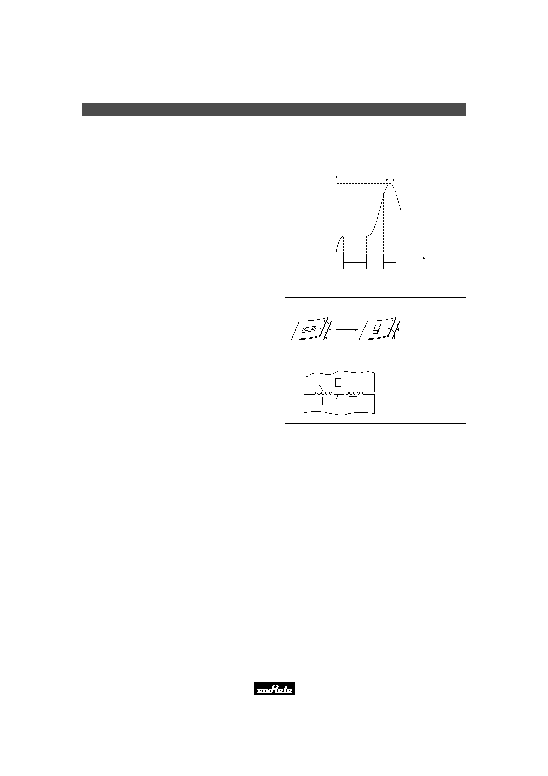
s Notice (Soldering and Mounting)
Filter is soldered one time within the following
temperature condition and then being placed in natural
condition for 4 hours.
1. Standard Reflow Soldering Condition
(1) Reflow
The component cannot be withstand washing.
2. Wash
Lead terminal is directly contacted with the tip of
soldering iron of 280
±
5
∞
C for 3.0 seconds
±
0.5 seconds,
and then being placed in natural condition for 4 hours.
(2) Soldering Iron
60
30
5 sec.
240
230
150
T
e
m
p
e
r
a
t
u
r
e
(
∞
C
)
Gradual
Cooling
Time (sec.)
s Notice (Handling)
1. The component may be damaged if excess mechanical
stress is applied to it mounted on the printed circuit
board.
2. Design layout of components on the PC board to
minimize the stress imposed on the wrap or flexure of the
board.
3. After installing chips, if solder is excessively applied to
the circuit board, mechanical stress will cause destruction
resistance characteristics to lower. To prevent this, be
extremly careful in determining shape and dimension
before designing the circuit board diagram.
4. When the positioning claws and pick up nozzle are worn,
the load is applied to the chip while positioning is
concentrated to one positioning accuracy, etc. Careful
checking and maintenance are necessary to prevent
unexpected trouble.
5. When correcting chips with a soldering iron, the tip of the
soldering iron should not directly touch the chip
component.
6. Cleaning or washing of the component is not acceptable
due to non sealed construction.
7. In case of covering filter with over coat, conditions such
as material of resin, cure temperature, and so on should
be evaluated well.
8. Accurate test circuit values are required to measure
electrical characteristics. It may be a cause of miss-
correlation if there is any deviation, especially stray
capacitance, from the test circuit in the specification.
[Component direction]
[Component layout close to board]
Put the compon-
ent lateral to
the direction in
which stress
acts.
Susceptibility to
stress is in the order
of;A>C>B
B
A
C
Slit
Perforation

Please read CAUTION and Notice in this catalog for safety. This catalog has only typical specifications. Therefore you are requested
to approve our product specification or to transact the approval sheet for product specification, before your ordering.
P25E3.pdf 01.10.17
6
2
CERAFILr(Filters/Traps/Discriminators) for TV/VCR
CERAFIL
r
Picture Band Low-Suprious SFSRA Series
As part of the environment protection activity, solder
for terminal plating and terminal-element connection
inside of ceramic filter SFSRA series contain no
lead(Pb).
This series also features thickness shear vibration
mode same as SFSRH series(current type), which
provides very low spurious response within video
signal band.
s Features
1. Excellent spurious suppression characteristics
within video signal band.
2. Available 4 pass bandwidth variation to meet
various requests.
3. Low profile (H=7.0mm max.)
4. Lead dimension : Improved mounting reliability
(cut & clinch) due to round terminal.
M
10.0 max.
7.0
(Ref.)
2.5
±
0.2
2.5
±
0.2
7
.
0
m
a
x
.
3
.
5
±
0
.
5
0
.
4
8
±
0
.
1
0
.
9
(
R
e
f
.
)
4
.
0
m
a
x
.
3--0.8
(3)
(2)
(1)
(in mm)
Part Number
Nominal Center
Frequency (fn)
(MHz)
3dB
Bandwidth
(kHz)
20dB
Bandwidth
(kHz)
Insertion
Loss
(dB)
Spurious
Attenuation(1)
(dB)
Spurious
Attenuation(2)
(dB)
Input/Output
Impedance
(ohm)
SFSRA4M50CF00-B0
4.500
fn
±
60 min.
600 max.
6.0 max.
30 min.
[within 0 to fn]
20 min.
[within fn to 7.0MHz]
1000
SFSRA4M50DF00-B0
4.500
fn
±
70 min.
750 max.
6.0 max.
30 min.
[within 0 to fn]
20 min.
[within fn to 7.0MHz]
1000
SFSRA4M50EF00-B0
4.500
fn
±
125 min.
850 max.
6.0 max.
25 min.
[within 0 to fn]
18 min.
[within fn to 7.0MHz]
1000
SFSRA5M50BF00-B0
5.500
fn
±
50 min.
400 max.
8.0 max.
30 min.
[within 0 to fn]
20 min.
[within fn to 7.57MHz]
600
SFSRA5M50CF00-B0
5.500
fn
±
60 min.
600 max.
6.0 max.
30 min.
[within 0 to fn]
20 min.
[within fn to7.5MHz]
600
SFSRA5M50DF00-B0
5.500
fn
±
80 min.
750 max.
6.0 max.
30 min.
[within 0 to fn]
20 min.
[within fn to 7.5MHz]
600
SFSRA5M74BF00-B0
5.742
fn
±
50 min.
400 max.
8.0 max.
30 min.
[within 0 to fn]
20 min.
[within fn to 8.0MHz]
600
SFSRA5M74CF00-B0
5.742
fn
±
60 min.
600 max.
6.0 max.
30 min.
[within 0 to fn]
20 min.
[within fn to 7.5MHz]
600
SFSRA6M00CF00-B0
6.000
fn
±
60 min.
600 max.
6.0 max.
30 min.
[within 0 to fn]
20 min.
[within fn to 8.0MHz]
470
SFSRA6M00DF00-B0
6.000
fn
±
80 min.
750 max.
6.0 max.
30 min.
[within 0 to fn]
20 min.
[within fn to 8.0MHz]
470
SFSRA6M50CF00-B0
6.500
fn
±
70 min.
650 max.
6.0 max.
30 min.
[within 0 to fn]
20 min.
[within fn to 8.5MHz]
470
SFSRA6M50DF00-B0
6.500
fn
±
80 min.
800 max.
6.0 max.
30 min.
[within 0 to fn]
20 min.
[within fn to 8.5MHz]
470

Please read CAUTION and Notice in this catalog for safety. This catalog has only typical specifications. Therefore you are requested
to approve our product specification or to transact the approval sheet for product specification, before your ordering.
P25E3.pdf 01.10.17
7
2
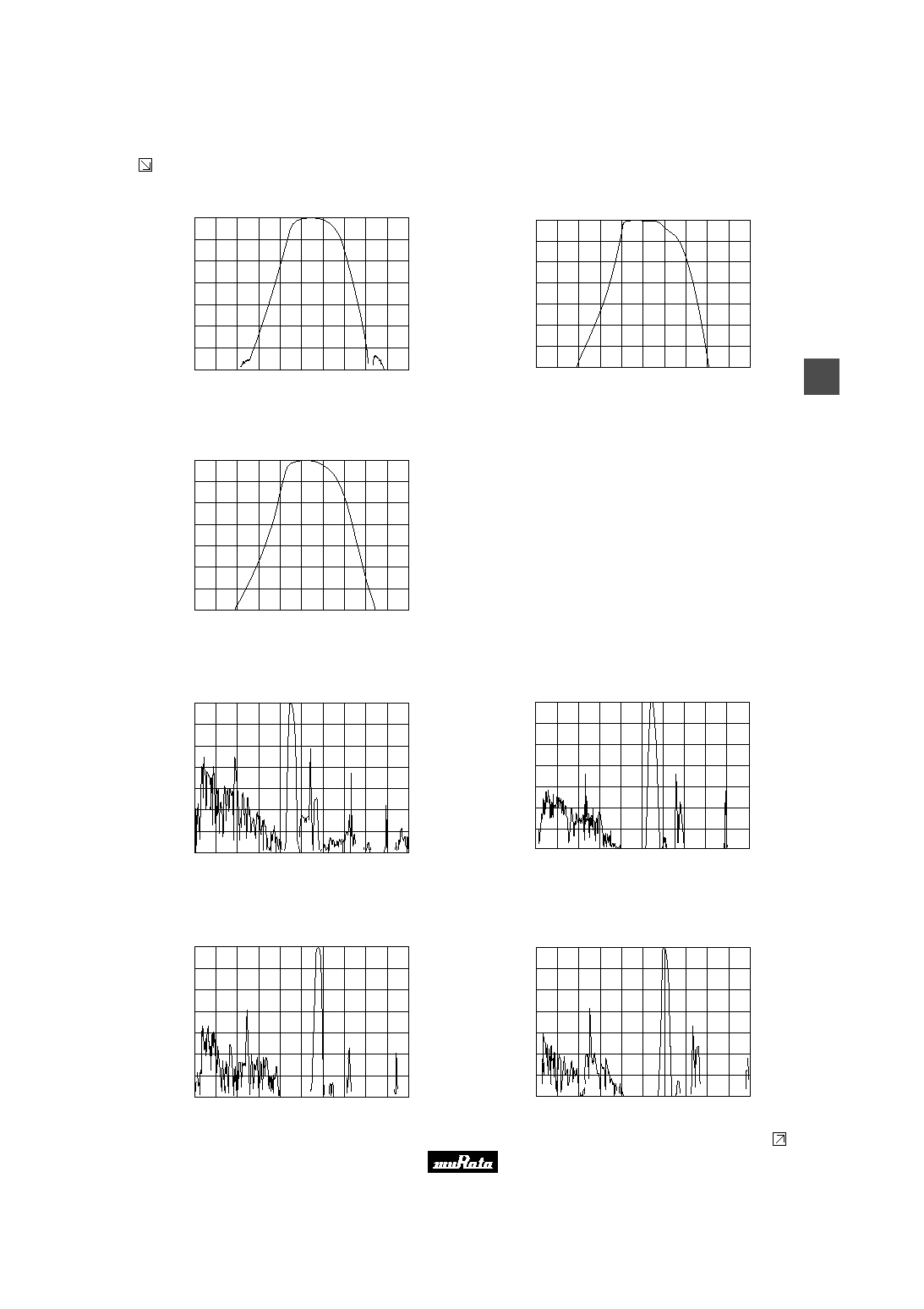
s Frequency Characteristics
SFSRA4M50CF00-B0
3.5
3.7
3.9
4.1
4.3
4.5
Frequency (MHz)
4.7
4.9
5.1
5.3
5.5
50
60
70
40
30
20
10
0
A
t
t
e
n
u
a
t
i
o
n
.
(
d
B
)
SFSRA4M50DF00-B0
3.5
3.7
3.9
4.1
4.3
4.5
Frequency (MHz)
4.7
4.9
5.1
5.3
5.5
50
60
70
40
30
20
10
0
A
t
t
e
n
u
a
t
i
o
n
.
(
d
B
)
SFSRA4M50EF00-B0
3.5
3.7
3.9
54
4.3
4.5
Frequency (MHz)
4.7
4.9
5.1
5.3
5.5
50
60
70
40
30
20
10
0
A
t
t
e
n
u
a
t
i
o
n
.
(
d
B
)
SFSRA5M50BF00-B0
4.5
4.7
4.9
5.1
5.3
5.5
Frequency (MHz)
5.7
5.9
6.1
6.3
6.5
50
60
70
40
30
20
10
0
A
t
t
e
n
u
a
t
i
o
n
.
(
d
B
)
SFSRA5M50CF00-B0
4.5
4.7
4.9
5.1
5.3
5.5
Frequency (MHz)
5.7
5.9
6.1
6.3
6.5
50
60
70
40
30
20
10
0
A
t
t
e
n
u
a
t
i
o
n
.
(
d
B
)
SFSRA5M50DF00-B0
4.5
4.7
4.9
5.1
5.3
5.5
Frequency (MHz)
5.7
5.9
6.1
6.3
6.5
50
60
70
40
30
20
10
0
A
t
t
e
n
u
a
t
i
o
n
.
(
d
B
)
SFSRA5M74BF00-B0
4.7
4.9
5.1
5.3
5.5
Frequency (MHz)
5.7
5.9
6.1
6.3
6.5
6.7
50
60
70
40
30
20
10
0
A
t
t
e
n
u
a
t
i
o
n
.
(
d
B
)
SFSRA5M74CF00-B0
4.7
4.9
5.1
5.3
5.5
Frequency (MHz)
5.7
5.9
6.1
6.3
6.5
6.7
50
60
70
40
30
20
10
0
A
t
t
e
n
u
a
t
i
o
n
.
(
d
B
)
Continued on the following page.

Please read CAUTION and Notice in this catalog for safety. This catalog has only typical specifications. Therefore you are requested
to approve our product specification or to transact the approval sheet for product specification, before your ordering.
P25E3.pdf 01.10.17
8
2
Continued from the preceding page.
s Frequency Characteristics
SFSRA6M00CF00-B0
5.0
5.2
5.4
5.6
5.8
6.0
6.2
6.4
6.6
6.8
7.0
50
60
70
40
30
20
10
0
A
t
t
e
n
u
a
t
i
o
n
(
d
B
)
Frequency (MHz)
SFSRA6M00DF00-B0
A
t
t
e
n
u
a
t
i
o
n
(
d
B
)
Frequency (MHz)
5.0
5.2
5.4
5.6
5.8
6.0
6.2
6.4
6.6
6.8
7.0
50
60
70
40
30
20
10
0
SFSRA6M50CF00-B0
A
t
t
e
n
u
a
t
i
o
n
(
d
B
)
Frequency (MHz)
5.5
5.7
5.9
6.1
6.3
6.5
6.7
6.9
7.1
7.3
7.5
50
60
70
40
30
20
10
0
SFSRA6M50DF00-B0
A
t
t
e
n
u
a
t
i
o
n
(
d
B
)
Frequency (MHz)
5.5
5.7
5.9
6.1
6.3
6.5
6.7
6.9
7.1
7.3
7.5
50
60
70
40
30
20
10
0
s Spurious Response
SFSRA4M50CF00-B0
0.0
1.0
2.0
3.0
4.0
5.0
Frequency (MHz)
6.0
7.0
8.0
9.0
10.0
50
60
70
40
30
20
10
0
A
t
t
e
n
u
a
t
i
o
n
.
(
d
B
)
SFSRA4M50DF00-B0
0.0
1.0
2.0
3.0
4.0
5.0
Frequency (MHz)
6.0
7.0
8.0
9.0
10.0
50
60
70
40
30
20
10
0
A
t
t
e
n
u
a
t
i
o
n
.
(
d
B
)
SFSRA4M50EF00-B0
0.0
1.0
2.0
3.0
4.0
5.0
Frequency (MHz)
6.0
7.0
8.0
9.0
10.0
50
60
70
40
30
20
10
0
A
t
t
e
n
u
a
t
i
o
n
.
(
d
B
)
SFSRA5M50BF00-B0
0.0
1.0
2.0
3.0
4.0
5.0
Frequency (MHz)
6.0
7.0
8.0
9.0
10.0
50
60
70
40
30
20
10
0
A
t
t
e
n
u
a
t
i
o
n
.
(
d
B
)
Continued on the following page.

Please read CAUTION and Notice in this catalog for safety. This catalog has only typical specifications. Therefore you are requested
to approve our product specification or to transact the approval sheet for product specification, before your ordering.
P25E3.pdf 01.10.17
9
2
Continued from the preceding page.
s Spurious Response
SFSRA5M50CF00-B0
0.0
1.0
2.0
3.0
4.0
5.0
Frequency (MHz)
6.0
7.0
8.0
9.0
10.0
50
60
70
40
30
20
10
0
A
t
t
e
n
u
a
t
i
o
n
.
(
d
B
)
0.0
1.0
2.0
3.0
4.0
5.0
Frequency (MHz)
6.0
7.0
8.0
9.0
10.0
50
60
70
40
30
20
10
0
A
t
t
e
n
u
a
t
i
o
n
.
(
d
B
)
SFSRA5M50DF00-B0
SFSRA5M74BF00-B0
0.0
1.0
2.0
3.0
4.0
5.0
Frequency (MHz)
6.0
7.0
8.0
9.0
10.0
50
60
70
40
30
20
10
0
A
t
t
e
n
u
a
t
i
o
n
.
(
d
B
)
SFSRA5M74CF00-B0
0.0
1.0
2.0
3.0
4.0
5.0
Frequency (MHz)
6.0
7.0
8.0
9.0
10.0
50
60
70
40
30
20
10
0
A
t
t
e
n
u
a
t
i
o
n
.
(
d
B
)
SFSRA6M00CF00-B0
0.0
1.0
2.0
3.0
4.0
5.0
Frequency (MHz)
6.0
7.0
8.0
9.0
10.0
50
60
70
40
30
20
10
0
A
t
t
e
n
u
a
t
i
o
n
.
(
d
B
)
SFSRA6M00DF00-B0
0.0
1.0
2.0
3.0
4.0
5.0
Frequency (MHz)
6.0
7.0
8.0
9.0
10.0
50
60
70
40
30
20
10
0
A
t
t
e
n
u
a
t
i
o
n
.
(
d
B
)
SFSRA6M50CF00-B0
0.0
1.0
2.0
3.0
4.0
5.0
Frequency (MHz)
6.0
7.0
8.0
9.0
10.0
50
60
70
40
30
20
10
0
A
t
t
e
n
u
a
t
i
o
n
.
(
d
B
)
SFSRA6M50DF00-B0
0.0
1.0
2.0
3.0
4.0
5.0
Frequency (MHz)
6.0
7.0
8.0
9.0
10.0
50
60
70
40
30
20
10
0
A
t
t
e
n
u
a
t
i
o
n
.
(
d
B
)
Continued on the following page.

Please read CAUTION and Notice in this catalog for safety. This catalog has only typical specifications. Therefore you are requested
to approve our product specification or to transact the approval sheet for product specification, before your ordering.
P25E3.pdf 01.10.17
10
2
Continued from the preceding page.
s Test Circuit
RF
Voltmeter
1
S.S.G.
Rg
R1
R2
C
3
2
Rg+R1=R2=Input and Output Impedance
C=10pF (Including stray capacitance and
input capacitance of RF voltmeter)
Please read CAUTION and Notice in this catalog for safety. This catalog has only typical specifications. Therefore you are requested
to approve our product specification or to transact the approval sheet for product specification, before your ordering.
P25E3.pdf 01.10.17
11
3
CERAFILr(Filters/Traps/Discriminators) for TV/VCR
CERAFIL
r
Low-profile SFSRL Series
SFSRL series are the Low-profile type of standard
SFSRA series.
s Features
1. Installed height is 6.0mm, making it well suited
for compact, thin sets.
2. Electrical char. and performance are the same as
those of SFSRA series.
3. 2 types, narrow and middle bandwidth, are prepared.
5
.
0
±
1
.
0
0.5
±
0.1
1.1
±
0.1
10.0 max.
6
.
0
m
a
x
.
M A R K I N G
E I A J
C O D E
4
.
0
m
a
x
.
(3) (2) (1)
0
.
3
±
0
.
1
2.5
±
0.2
±
0.2
2.5
(in mm)
Part Number
Nominal Center
Frequency (fn)
(MHz)
3dB
Bandwidth
(kHz)
20dB
Bandwidth
(kHz)
Insertion
Loss
(dB)
Spurious
Attenuation(1)
(dB)
Spurious
Attenuation(2)
(dB)
Input/Output
Impedance
(ohm)
SFSRL4M50CF00-B0
4.500
fn
±
60 min.
600 max.
6.0 max.
30 min.
[within 0 to fn]
15 min.
[within fn to 7.0MHz]
1000
SFSRL4M50DF00-B0
4.500
fn
±
70 min.
750 max.
6.0 max.
30 min.
[within 0 to fn]
15 min.
[within fn to 5.7MHz]
1000
SFSRL5M50CF00-B0
5.500
fn
±
60 min.
600 max.
6.0 max.
30 min.
[within 0 to fn]
15 min.
[within fn to 7.0MHz]
600
SFSRL5M50DF00-B0
5.500
fn
±
80 min.
750 max.
6.0 max.
30 min.
[within 0 to fn]
15 min.
[within fn to 7.0MHz]
600
SFSRL6M00CF00-B0
6.000
fn
±
60 min.
600 max.
6.0 max.
30 min.
[within 0 to fn]
15 min.
[within fn to 7.5MHz]
470
SFSRL6M00DF00-B0
6.000
fn
±
80 min.
750 max.
6.0 max.
30 min.
[within 0 to fn]
15 min.
[within fn to 7.5MHz]
470
SFSRL6M50CF00-B0
6.500
fn
±
70 min.
650 max.
6.0 max.
30 min.
[within 0 to fn]
15 min.
[within fn to 8.5MHz]
470
SFSRL6M50DF00-B0
6.500
fn
±
80 min.
800 max.
6.0 max.
30 min.
[within 0 to fn]
15 min.
[within fn to 8.0MHz]
470
s Frequency Characteristics
SFSRL4M50CF00-B0
0
10
20
30
40
50
60
70
3.7
3.5
3.9
4.1
4.3
4.5
4.7
4.9
5.1
5.3
5.5
Frequency (MHz)
A
t
t
e
n
u
a
t
i
o
n
(
d
B
)
SFSRL4M50DF00-B0
3.5
3.7
3.9
4.1
4.3
4.5
4.7
4.9
5.1
5.3
5.5
0
10
20
30
40
50
60
70
Frequency (MHz)
A
t
t
e
n
u
a
t
i
o
n
(
d
B
)
Continued on the following page.

Please read CAUTION and Notice in this catalog for safety. This catalog has only typical specifications. Therefore you are requested
to approve our product specification or to transact the approval sheet for product specification, before your ordering.
P25E3.pdf 01.10.17
12
3
Continued from the preceding page.
s Frequency Characteristics
SFSRL5M50CF00-B0
0
10
20
30
40
50
60
70
4.7
4.5
4.9
5.1
5.3
5.5
5.7
5.9
6.1
6.3
6.5
Frequency (MHz)
A
t
t
e
n
u
a
t
i
o
n
(
d
B
)
SFSRL5M50DF00-B0
0
10
20
30
40
50
60
70
A
t
t
e
n
u
a
t
i
o
n
(
d
B
)
4.5
4.7
4.9
5.1
5.3
5.5
Frequency (MHz)
5.7
5.9
6.1
6.3
6.5
SFSRL6M00CF00-B0
0
10
20
30
40
50
60
70
Frequency (MHz)
A
t
t
e
n
u
a
t
i
o
n
(
d
B
)
5.0
5.6
5.8
6.2
6.6
5.2
5.4
6.0
6.4
6.8
7.0
SFSRL6M00DF00-B0
0
10
20
30
40
50
60
70
5.2
5.0
5.4
5.6
5.8
6.0
6.2
6.4
6.6
6.8
7.0
Frequency (MHz)
A
t
t
e
n
u
a
t
i
o
n
(
d
B
)
SFSRL6M50CF00-B0
0
10
20
30
40
50
60
70
Frequency (MHz)
A
t
t
e
n
u
a
t
i
o
n
(
d
B
)
5.5
6.1
6.3
6.7
7.1
5.7
5.9
6.5
6.9
7.3
7.5
SFSRL6M50DF00-B0
0
10
20
30
40
50
60
70
5.7
5.5
5.9
6.1
6.3
6.5
6.7
6.9
7.1
7.3
7.5
Frequency (MHz)
A
t
t
e
n
u
a
t
i
o
n
(
d
B
)
s Spurious Response
SFSRL4M50CF00-B0
0
10
20
30
40
50
60
70
1.0
0.0
2.0
3.0
4.0
5.0
6.0
7.0
8.0
9.0
10.0
Frequency (MHz)
A
t
t
e
n
u
a
t
i
o
n
(
d
B
)
SFSRL4M50DF00-B0
0.0
1.0
2.0
3.0
4.0
5.0
6.0
7.0
8.0
9.0
10.0
0
10
20
30
40
50
60
70
Frequency (MHz)
A
t
t
e
n
u
a
t
i
o
n
(
d
B
)
Continued on the following page.

Please read CAUTION and Notice in this catalog for safety. This catalog has only typical specifications. Therefore you are requested
to approve our product specification or to transact the approval sheet for product specification, before your ordering.
P25E3.pdf 01.10.17
13
3
Continued from the preceding page.
s Spurious Response
SFSRL5M50CF00-B0
0
10
20
30
40
50
60
70
1.0
0.0
2.0
3.0
4.0
5.0
6.0
7.0
8.0
9.0
10.0
Frequency (MHz)
A
t
t
e
n
u
a
t
i
o
n
(
d
B
)
SFSRL5M50DF00-B0
0
10
20
30
40
50
60
70
A
t
t
e
n
u
a
t
i
o
n
(
d
B
)
0.0
1.0
2.0
3.0
4.0
5.0
6.0
7.0
8.0
9.0 10.0
Frequency (MHz)
SFSRL6M00CF00-B0
0
10
20
30
40
50
60
70
Frequency (MHz)
A
t
t
e
n
u
a
t
i
o
n
(
d
B
)
0.0
3.0
4.0
6.0
8.0
1.0
2.0
5.0
7.0
9.0
10.0
SFSRL6M00DF00-B0
0
10
20
30
40
50
60
70
1.0
0.0
2.0
3.0
4.0
5.0
6.0
7.0
8.0
9.0
10.0
Frequency (MHz)
A
t
t
e
n
u
a
t
i
o
n
(
d
B
)
SFSRL6M50CF00-B0
0
10
20
30
40
50
60
70
Frequency (MHz)
A
t
t
e
n
u
a
t
i
o
n
(
d
B
)
0.0
3.0
4.0
6.0
8.0
1.0
2.0
5.0
7.0
9.0
10.0
SFSRL6M50DF00-B0
0
10
20
30
40
50
60
70
1.0
0.0
2.0
3.0
4.0
5.0
6.0
7.0
8.0
9.0
10.0
Frequency (MHz)
A
t
t
e
n
u
a
t
i
o
n
(
d
B
)
s Test Circuit
RF
Voltmeter
1
S.S.G.
Rg
R1
R2
C
3
2
Rg+R1=R2=Input and Output Impedance
C=10pF (Including stray capacitance and
input capacitance of RF voltmeter)

Please read CAUTION and Notice in this catalog for safety. This catalog has only typical specifications. Therefore you are requested
to approve our product specification or to transact the approval sheet for product specification, before your ordering.
P25E3.pdf 01.10.17
14
4
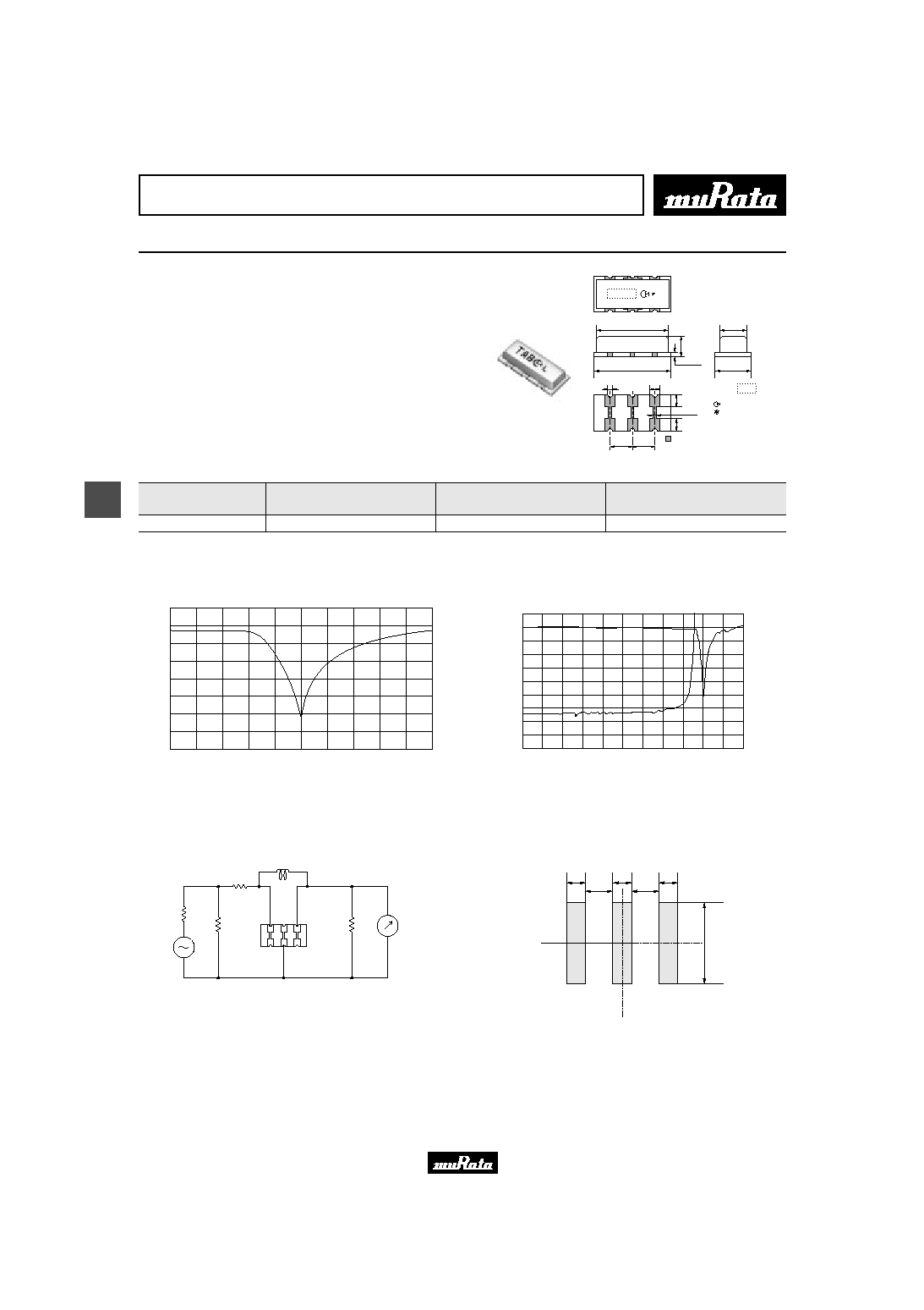
CERAFILr(Filters/Traps/Discriminators) for TV/VCR
CERAFIL
r
High-selectivity Type SFTRD Series
Ceramic filter SFTRD_AF series are high selectivity
filter which involves 3-elements filter unit.
s Features
1. Excellent shape factor.
2. Good performance for spurious suppression.
3. Four-terminals type.
4. Suitable for 2 channel Multi-sound TV of Germany
and Korea.
(1)
(2)
(3)
(4)
T
15.0
±
2.0
7
.
5
±
2
.
0
0.5
±
0.1
5
.
0
±
1
.
0
1.4
±
0.1
3
.
0
±
1
.
0
2.5
±
0.2
7.5
±
0.2
0
.
3
±
0
.
1
2.5
±
0.2
A
E I A J
C O D E
(in mm)
Part Number
Nominal Center
Frequency (fn)
(MHz)
3dB
Bandwidth
(kHz)
20dB
Bandwidth
(kHz)
Insertion
Loss
(dB)
Spurious
Attenuation(1)
(dB)
Spurious
Attenuation(2)
(dB)
Input/Output
Impedance
(ohm)
SFTRD4M50AF00-B0
4.500
fn
±
40 min.
370 max.
10.0 max.
50 min.
[within fn-1.0MHz to fn]
40 min.
[within fn to fn+0.8MHz]
1000
SFTRD5M50AF00-B0
5.500
fn
±
50 min.
350 max.
9.0 max.
50 min.
[within fn-1.0MHz to fn]
50 min.
[within fn to fn+1.0MHz]
600
SFTRD5M74AF00-B0
5.742
fn
±
50 min.
350 max.
9.0 max.
50 min.
[within fn-1.0MHz to fn]
50 min.
[within fn to fn+1.0MHz]
600
SFTRD6M00AF00-B0
6.000
fn
±
50 min.
400 max.
9.0 max.
50 min.
[within fn-1.0MHz to fn]
50 min.
[within fn to fn+1.0MHz]
470
SFTRD6M50AF00-B0
6.500
fn
±
50 min.
400 max.
9.0 max.
50 min.
[within fn-1.0MHz to fn]
50 min.
[within fn to fn+1.0MHz]
470
s Frequency Characteristics
SFTRD4M50AF00-B0
0
10
20
30
40
50
60
70
4.1
4.0
4.2
4.3
4.4
4.5
4.6
4.7
4.8
4.9
5.0
Frequency (MHz)
A
t
t
e
n
u
a
t
i
o
n
(
d
B
)
SFTRD5M50AF00-B0
4.5
4.7
4.9
5.1
5.3
5.5
5.7
5.9
6.1
6.3
6.5
0
10
20
30
40
50
60
70
Frequency (MHz)
A
t
t
e
n
u
a
t
i
o
n
(
d
B
)
Continued on the following page.
Please read CAUTION and Notice in this catalog for safety. This catalog has only typical specifications. Therefore you are requested
to approve our product specification or to transact the approval sheet for product specification, before your ordering.
P25E3.pdf 01.10.17
15
4
Continued from the preceding page.
s Frequency Characteristics
SFTRD5M74AF00-B0
0
10
20
30
40
50
60
70
Frequency (MHz)
A
t
t
e
n
u
a
t
i
o
n
(
d
B
)
5.2
5.5
5.6
5.8
6.0
5.3
5.4
5.7
5.9
6.1
6.2
SFTRD6M00AF00-B0
0
10
20
30
40
50
60
70
Frequency (MHz)
A
t
t
e
n
u
a
t
i
o
n
(
d
B
)
5.5
5.8
5.9
6.1
6.3
5.6
5.7
6.0
6.2
6.4
6.5
SFTRD6M50AF00-B0
0
10
20
30
40
50
60
70
6.1
6.0
6.2
6.3
6.4
6.5
6.6
6.7
6.8
6.9
7.0
Frequency (MHz)
A
t
t
e
n
u
a
t
i
o
n
(
d
B
)
s Spurious Response
SFTRD4M50AF00-B0
0
10
20
30
40
50
60
70
1.0
0.0
2.0
3.0
4.0
5.0
6.0
7.0
8.0
9.0
10.0
Frequency (MHz)
A
t
t
e
n
u
a
t
i
o
n
(
d
B
)
SFTRD5M50AF00-B0
1.0
2.0
3.0
4.0
5.0
6.0
7.0
8.0
9.0
10.0
0.0
0
10
20
30
40
50
60
70
Frequency (MHz)
A
t
t
e
n
u
a
t
i
o
n
(
d
B
)
SFTRD5M74AF00-B0
0
10
20
30
40
50
60
70
Frequency (MHz)
A
t
t
e
n
u
a
t
i
o
n
(
d
B
)
0.0
3.0
4.0
6.0
8.0
1.0
2.0
5.0
7.0
9.0
10.0
SFTRD6M00AF00-B0
0
10
20
30
40
50
60
70
Frequency (MHz)
A
t
t
e
n
u
a
t
i
o
n
(
d
B
)
0.0
3.0
4.0
6.0
8.0
1.0
2.0
5.0
7.0
9.0
10.0
Continued on the following page.

Please read CAUTION and Notice in this catalog for safety. This catalog has only typical specifications. Therefore you are requested
to approve our product specification or to transact the approval sheet for product specification, before your ordering.
P25E3.pdf 01.10.17
16
4
Continued from the preceding page.
s Spurious Response
SFTRD6M50AF00-B0
0
10
20
30
40
50
60
70
1.0
0.0
2.0
3.0
4.0
5.0
6.0
7.0
8.0
9.0
10.0
Frequency (MHz)
A
t
t
e
n
u
a
t
i
o
n
(
d
B
)
s Test Circuit
(1) (2)
(3)
C
S.S.G
R.F.
Voltmeter
Rg
R
1
R
2
Rg + R
1
= R
2
= 330
C = 10pF (Including stray capacitance and input
capacitance of RF voltmeter.)
(1) : Input
(2),(3) : Ground
(3) : Output
(4)

Please read CAUTION and Notice in this catalog for safety. This catalog has only typical specifications. Therefore you are requested
to approve our product specification or to transact the approval sheet for product specification, before your ordering.
P25E3.pdf 01.10.17
17
5
CERAFILr(Filters/Traps/Discriminators) for TV/VCR
CERAFIL
r
Chroma Signal SFSRA/H/L Series
Chroma signals frequency conversion process is
involved in VCRs video signal processing circuit.
These SFSRA/SFSRH/SFSRL series are suitable for B.P.F.
s Features
1. Frequency adjustment free.
2. Responsible for VHS. 8mm VCR system.
M
10.0 max.
7.0
(Ref.)
2.5
±
0.2
2.5
±
0.2
7
.
0
m
a
x
.
3
.
5
±
0
.
5
0
.
4
8
±
0
.
1
0
.
9
(
R
e
f
.
)
4
.
0
m
a
x
.
3--0.8
(3)
(2)
(1)
(in mm)
SFSRA Series
8
.
0
m
a
x
.
4
.
0
m
a
x
.
(3)
(2)
(1)
1.38
±
0.2
5
.
0
±
1
.
0
0.5
±
0.1
1.7
±
0.1
0
.
3
±
0
.
1
2.5
±
0.2
2.5
±
0.2
10.0 max.
F4.5D
M
(in mm)
(1) Input
(2) Ground
(3) Output
SFSRH Series
5
.
0
±
1
.
0
0.5
±
0.1
1.1
±
0.1
10.0 max.
6
.
0
m
a
x
.
M A R K I N G
E I A J
C O D E
4
.
0
m
a
x
.
(3) (2) (1)
0
.
3
±
0
.
1
2.5
±
0.2
±
0.2
2.5
(in mm)
SFSRL Series
Part Number
Nominal Center
Frequency (fn)
(MHz)
3dB
Bandwidth
(kHz)
20dB
Bandwidth
(kHz)
Insertion
Loss
(dB)
Spurious
Attenuation(1)
(dB)
Spurious
Attenuation(2)
(dB)
Input/Output
Impedance
(ohm)
SFSRA4M43CF00-B0
4.430
fn
±
60 min.
600 max.
6.0 max.
30 min.
[within 0 to fn]
20 min.
[within fn to 7.0MHz]
1000
SFSRH3M58CF00-B0
3.580
fn
±
40 min.
530 max.
6.0 max.
25 min.
[within 0 to fn]
15 min.
[within fn to 6.0MHz]
1000
SFSRL4M32DF00-B0
4.320
fn
±
70 min.
750 max.
6.0 max.
30 min.
[within 0 to fn]
15 min.
[within fn to 5.5MHz]
1000
SFSRL5M17DF00-B0
5.170
fn
±
70 min.
750 max.
7.5 max.
30 min.
[within 0 to fn]
15 min.
[within fn to 7.0MHz]
600
s Frequency Characteristics
SFSRA4M43CF00-B0
70
4.7
4.5
4.3
Frequency (MHz)
A
t
t
e
n
u
a
t
i
o
n
(
d
B
)
4.1
5.3
5.5
5.1
4.9
3.9
3.5
3.7
60
50
40
30
20
10
0
SFSRH3M58CF00-B0
70
3.9
3.7
3.5
Frequency (MHz)
A
t
t
e
n
u
a
t
i
o
n
(
d
B
)
3.3
4.5
4.7
4.3
4.1
3.1
2.7
2.9
60
50
40
30
20
10
0
Continued on the following page.

Please read CAUTION and Notice in this catalog for safety. This catalog has only typical specifications. Therefore you are requested
to approve our product specification or to transact the approval sheet for product specification, before your ordering.
P25E3.pdf 01.10.17
18
5
Continued from the preceding page.
s Frequency Characteristics
SFSRL4M32DF00-B0
70
3.3
4.7
4.5
4.3
Frequency (MHz)
A
t
t
e
n
u
a
t
i
o
n
(
d
B
)
4.1
5.3
5.1
4.9
3.9
3.5
3.7
60
50
40
30
20
10
0
SFSRL5M17DF00-B0
0
10
20
30
40
50
60
70
4.4
4.2
4.6
4.8
5.0
5.2
5.4
5.6
5.8
6.0
6.2
Frequency (MHz)
A
t
t
e
n
u
a
t
i
o
n
(
d
B
)
s Spurious Response
SFSRA4M43CF00-B0
70
0.0
7.0
6.0
5.0
4.0
10.0
9.0
8.0
3.0
1.0
2.0
60
50
40
30
20
10
0
Frequency (MHz)
A
t
t
e
n
u
a
t
i
o
n
(
d
B
)
SFSRH3M58CF00-B0
70
0.0
7.0
6.0
5.0
4.0
10.0
9.0
8.0
3.0
1.0
2.0
60
50
40
30
20
10
0
Frequency (MHz)
A
t
t
e
n
u
a
t
i
o
n
(
d
B
)
SFSRL4M32DF00-B0
70
0.0
7.0
6.0
5.0
4.0
10.0
9.0
8.0
3.0
1.0
2.0
60
50
40
30
20
10
0
Frequency (MHz)
A
t
t
e
n
u
a
t
i
o
n
(
d
B
)
SFSRL5M17DF00-B0
0
10
20
30
40
50
60
70
1.0
0.0
2.0
3.0
4.0
5.0
6.0
7.0
8.0
9.0
10.0
Frequency (MHz)
A
t
t
e
n
u
a
t
i
o
n
(
d
B
)
s Test Circuit
RF
Voltmeter
1
S.S.G.
Rg
R1
R2
C
3
2
Rg+R1=R2=Input and Output Impedance
C=10pF (Including stray capacitance and
input capacitance of RF voltmeter)

Please read CAUTION and Notice in this catalog for safety. This catalog has only typical specifications. Therefore you are requested
to approve our product specification or to transact the approval sheet for product specification, before your ordering.
P25E3.pdf 01.10.17
CERAFIL
r
Lead Type Notice
19
5
s Notice (Soldering and Mounting)
The component cannot be withstand washing.
s Notice (Handling)
1. Do not use this product with bend. The component
may be damaged if excess mechanical stress is
applied to it mounted on the printed circuit board.
2. The component may be damaged when an excess stress
will be applied.
3. All kinds of re-flow soldering must not be applied
on the component.
4. Do not clean or wash the component as it is not
hermetically sealed.
5. Please contact Murata or Murata representative for
soldering condition, in case of using lead free
solder.
6. Do not use strong acidity flux, more than 0.2wt%
chlorine content, in flow soldering.
7. In case of covering filter with over coat,
conditions such as material of resin, cure
temperature, and so on should be evaluated well.
8. Accurate test circuit values are required to
measure electrical characteristics. It may be a
cause of miss-correlation if there is any deviation,
especially stray capacitance, from the test circuit
in the specification.
Please read CAUTION and Notice in this catalog for safety. This catalog has only typical specifications. Therefore you are requested
to approve our product specification or to transact the approval sheet for product specification, before your ordering.
P25E3.pdf 01.10.17
20
6
CERAFILr(Filters/Traps/Discriminators) for TV/VCR
Ceramic Traps Chip Type TPSKA Series
SMD ceramic trap TPSKA_B is small and thin SMD trap
sealed with a metal cap. Recommended for LCD-TVs, and
small and thin tuners.
s Features
1. High attenuation and high performance group
delay time.
2. Small and thin pakage.
3. Reflow-solderable.
(1) : Input
(2) : Ground
(3) : Output
Marking : TAB
: Vender's Code
: EIAJ Monthly code
7.9
±
0.2
3.0
±
0.1
8.5
±
0.2
3.8
±
0.2
1.8
±
0.2
0.5
±
0.1
0.6
±
0.2
1.0
±
0.1
1.3
±
0.2
2.5
±
0.2 2.5
±
0.2
0.3
±
0.1
1.3
±
0.2
(1)
(2)
(3)
Electrode
in mm
Part Number
Nominal Center
Frequency (fn1)
(MHz)
Attenuation
(at fn1)
(dB)
30dB Attenuation
BW (fn1)
(kHz)
TPSKA4M50B00-R1
4.500
35 min.
50 min.
s Frequency Characteristics
A
t
t
e
n
u
a
t
i
o
n
(
d
B
)
Frequency (MHz)
4.0
4.2
4.1
4.3
4.5
4.7
4.9
4.4
4.6
4.8
5.0
0
10
20
30
40
50
60
70
s Spurious Response
A
t
t
e
n
u
a
t
i
o
n
(
d
B
)
Frequency (MHz)
0
1.0
2.0
3.0
4.0
5.0
G
.
D
.
T
.
(
n
s
e
c
)
0
10
20
30
40
50
60
70
80
700
600
500
400
300
200
100
0
s Test Circuit
RF
Voltmeter
Rg
R1
L
S.S.G.
Rg=50
R1=330
R2=1.0k
L=15
µ
H
50
R2
s Standard Land Pattern Dimensions
1.0
1.0
1.5
1.5
4
.
8
1.0

Please read CAUTION and Notice in this catalog for safety. This catalog has only typical specifications. Therefore you are requested
to approve our product specification or to transact the approval sheet for product specification, before your ordering.
P25E3.pdf 01.10.17
21
7
CERAFILr(Filters/Traps/Discriminators) for TV/VCR
Double Trap Chip Type TPWKA Series
SMD ceramic trap TPWKA is small and thin SMD trap
sealed with a metal cap. Recommended for LCD-TVs, and
small and thin tuners.
This series consist of 2 wafers with 2 trap
frequencies. Recommended for Multi standard set.
s Features
1. Good performance of attenuation.
2. Small and thin package.
3. Reflow-solderable.
M
7.9
±
0.2
4.2
±
0.1
8.5
±
0.2
5.0
±
0.2
0.4
±
0.2
1.0
±
0.1
0.3
±
0.1
0
.
4
±
0
.
1
1
.
5
±
0
.
2
1
.
3
±
0
.
2
1
.
3
±
0
.
2
2.5
±
0.2 2.5
±
0.2
: Electrode
(1) : Input or Output
(2) : Ground
(3) : Output or Input
(in mm)
(1)
(2)
(3)
Part Number
Nominal Center
Frequency (fn1)
(MHz)
Nominal Center
Frequency (fn2)
(MHz)
Attenuation
(at fn1)
(dB)
Attenuation
(at fn2)
(dB)
30dB Attenuation
BW (fn1)
(kHz)
TPWKA5M50B04-R1
5.500
5.742
30 min.
30 min.
50 min.
s Frequency Characteristics
4.5
4.7
4.9
5.1
5.3
5.5
5.7
5.9
6.1
6.3
6.5
50
60
70
40
30
20
10
0
A
t
t
e
n
u
a
t
i
o
n
.
(
d
B
)
Frequency (MHz)
s Spurious Response
0
1.0
2.0
3.0
4.0
5.0
6.0
7.0
8.0
9.0
10.0
0
200
400
600
800
50
60
70
40
30
20
10
0
G
.
D
.
T
.
(
n
e
s
c
)
A
t
t
e
n
u
a
t
i
o
n
.
(
d
B
)
Frequency (MHz)
s Test Circuit
50
L = 8.2
µ
H
RF
Voltmeter
R1
R2
Rg
Rg = 50
R1 = 150
R2 = 330
C2 = 10pF (Including stray capacitance and input capacitance of RF voltmeter)
L
S.S.G.
C2
s Standard Land Pattern Dimensions
1.2
1.3
1.3
1.2
1.2
1
.
9
1
.
9
5
.
8
(in mm)
Please read CAUTION and Notice in this catalog for safety. This catalog has only typical specifications. Therefore you are requested
to approve our product specification or to transact the approval sheet for product specification, before your ordering.
P25E3.pdf 01.10.17
Ceramic Trap Chip Type Notice
22
7
s Notice (Soldering and Mounting)
Trap is soldered one time within the following
temperature condition and then being placed in natural
condition for 4 hours.
1. Standard Reflow Soldering Condition
(1) Reflow
The component cannot be withstand washing.
2. Wash
Lead terminal is directly contacted with the tip of
soldering iron of 280
±
5
∞
C for 3.0 seconds
±
0.5 seconds,
and then being placed in natural condition for 4 hours.
(2) Soldering Iron
60
30
5 sec.
240
230
150
T
e
m
p
e
r
a
t
u
r
e
(
∞
C
)
Gradual
Cooling
Time (sec.)
s Notice (Handling)
1. The component may be damaged if excess mechanical
stress is applied to it mounted on the printed circuit
board.
2. Design layout of components on the PC board to
minimize the stress imposed on the wrap or flexure of the
board.
3. After installing chips, if solder is excessively applied to
the circuit board, mechanical stress will cause destruction
resistance characteristics to lower. To prevent this, be
extremly careful in determining shape and dimension
before designing the circuit board diagram.
4. When the positioning claws and pick up nozzle are worn,
the load is applied to the chip while positioning is
concentrated to one positioning accuracy, etc. Careful
checking and maintenance are necessary to prevent
unexpected trouble.
5. When correcting chips with a soldering iron, the tip of the
soldering iron should not directly touch the chip
component.
6. Cleaning or washing of the component is not acceptable
due to non sealed construction.
7. In case of covering filter with over coat, conditions such
as material of resin, cure temperature, and so on should
be evaluated well.
8. Accurate test circuit values are required to measure
electrical characteristics. It may be a cause of miss-
correlation if there is any deviation, especially stray
capacitance, from the test circuit in the specification.
[Component direction]
[Component layout close to board]
Put the compon-
ent lateral to
the direction in
which stress
acts.
Susceptibility to
stress is in the order
of;A>C>B
B
A
C
Slit
Perforation

Please read CAUTION and Notice in this catalog for safety. This catalog has only typical specifications. Therefore you are requested
to approve our product specification or to transact the approval sheet for product specification, before your ordering.
P25E3.pdf 01.10.17
23
8
CERAFILr(Filters/Traps/Discriminators) for TV/VCR
Ceramic Traps Three-terminals TPSRA Series
As part of the environment protection activity, solder
for terminal plating and terminal-element connection
inside of ceramic filter TPSRA series contain no
lead(Pb).
This series consist of 2 trap element on one wafer.
Suitable for the sound IF trap of CTV/VCR.
s Features
1. Good performance of attenuation.
2. Shape factor can be changed by the value of
Inductor "L".
3. Three-terminals type.
4. Low profile (H=7.0mm max.).
5. Lead dimension:
Improved mounting reliability(cut & clinch) due to
round terminal.
M
10.0 max.
7.0
(Ref.)
2.5
±
0.2
2.5
±
0.2
7
.
0
m
a
x
.
3
.
5
±
0
.
5
0
.
4
8
±
0
.
1
0
.
9
(
R
e
f
.
)
4
.
0
m
a
x
.
3--0.8
(in mm)
Part Number
Nominal Center
Frequency (fn1)
(MHz)
Attenuation
(at fn1)
(dB)
30dB Attenuation
BW (fn1)
(kHz)
TPSRA4M50B00-B0
4.500
35 min.
50 min.
TPSRA4M50C00-B0
4.500
30 min.
-
TPSRA5M50B00-B0
5.500
35 min.
70 min.
TPSRA5M74B00-B0
5.742
35 min.
70 min.
TPSRA6M00B00-B0
6.000
35 min.
70 min.
TPSRA6M50B00-B0
6.500
35 min.
70 min.
s Frequency Characteristics
TPSRA4M50B00-B0
50
60
70
40
30
20
10
0
A
t
t
e
n
u
a
t
i
o
n
(
d
B
)
Frequency (MHz)
4.0
4.1
4.2
4.3
4.4
4.5
4.6
4.7
4.8
4.9
5.0
TPSRA4M50C00-B0
50
60
70
40
30
20
10
0
A
t
t
e
n
u
a
t
i
o
n
(
d
B
)
Frequency (MHz)
4.0
4.1
4.2
4.3
4.4
4.5
4.6
4.7
4.8
4.9
5.0
Continued on the following page.

Please read CAUTION and Notice in this catalog for safety. This catalog has only typical specifications. Therefore you are requested
to approve our product specification or to transact the approval sheet for product specification, before your ordering.
P25E3.pdf 01.10.17
24
8
Continued from the preceding page.
s Frequency Characteristics
TPSRA5M50B00-B0
5.0
5.2
5.3
5.1
5.4
5.5
5.6
5.7
5.9
5.8
6.0
50
60
70
40
30
20
10
0
A
t
t
e
n
u
a
t
i
o
n
(
d
B
)
Frequency (MHz)
TPSRA5M74B00-B0
5.2
5.4
5.5
5.3
5.6
5.7
5.8
5.9
6.1
6.0
6.2
50
60
70
40
30
20
10
0
A
t
t
e
n
u
a
t
i
o
n
(
d
B
)
Frequency (MHz)
TPSRA6M00B00-B0
5.5
5.7
5.8
5.6
5.9
6.0
6.1
6.2
6.4
6.3
6.5
50
60
70
40
30
20
10
0
A
t
t
e
n
u
a
t
i
o
n
(
d
B
)
Frequency (MHz)
TPSRA6M50B00-B0
6.0
6.2
6.3
6.1
6.4
6.5
6.6
6.7
6.9
6.8
7.0
50
60
70
40
30
20
10
0
A
t
t
e
n
u
a
t
i
o
n
(
d
B
)
Frequency (MHz)
s Spurious Response
TPSRA4M50B00-B0
0
1.0
2.0
3.0
4.0
5.0
6.0
7.0
8.0
9.0
10.0
0
200
400
600
800
50
60
70
40
30
20
10
0
G
.
D
.
T
.
(
n
e
s
c
)
A
t
t
e
n
u
a
t
i
o
n
.
(
d
B
)
Frequency (MHz)
TPSRA4M50C00-B0
0
1.0
2.0
3.0
4.0
5.0
6.0
7.0
8.0
9.0
10.0
0
200
400
600
800
50
60
70
40
30
20
10
0
G
.
D
.
T
.
(
n
e
s
c
)
A
t
t
e
n
u
a
t
i
o
n
.
(
d
B
)
Frequency (MHz)
TPSRA5M50B00-B0
0
1.0
2.0
3.0
4.0
5.0
6.0
7.0
8.0
9.0
10.0
0
200
400
600
800
50
60
70
40
30
20
10
0
G
.
D
.
T
.
(
n
e
s
c
)
A
t
t
e
n
u
a
t
i
o
n
.
(
d
B
)
Frequency (MHz)
TPSRA5M74B00-B0
0
1.0
2.0
3.0
4.0
5.0
6.0
7.0
8.0
9.0
10.0
0
200
400
600
800
50
60
70
40
30
20
10
0
G
.
D
.
T
.
(
n
e
s
c
)
A
t
t
e
n
u
a
t
i
o
n
.
(
d
B
)
Frequency (MHz)
Continued on the following page.

Please read CAUTION and Notice in this catalog for safety. This catalog has only typical specifications. Therefore you are requested
to approve our product specification or to transact the approval sheet for product specification, before your ordering.
P25E3.pdf 01.10.17
25
8
Continued from the preceding page.
s Spurious Response
TPSRA6M00B00-B0
0
1.0
2.0
3.0
4.0
5.0
6.0
7.0
8.0
9.0
10.0
0
200
400
600
800
50
60
70
40
30
20
10
0
G
.
D
.
T
.
(
n
e
s
c
)
A
t
t
e
n
u
a
t
i
o
n
.
(
d
B
)
Frequency (MHz)
TPSRA6M50B00-B0
0
1.0
2.0
3.0
4.0
5.0
6.0
7.0
8.0
9.0
10.0
0
200
400
600
800
50
60
70
40
30
20
10
0
G
.
D
.
T
.
(
n
e
s
c
)
A
t
t
e
n
u
a
t
i
o
n
.
(
d
B
)
Frequency (MHz)
s Test Circuit
TPSRA4M50B00-B0
Rg=50ohm
S.S.G.
220ohm
8.2
µ
H
5
0
o
h
m
2
.
2
K
o
h
m
R.F.
Voltmeter
TPSRA4M50C00-B0
R.F.
Voltmeter
1
K
o
h
m
5
0
o
h
m
15
µ
H
Rg=50ohm
S.S.G.
330ohm
TPSRA5M50/5M74/6M00/6M50B00-B0
Rg=50ohm
S.S.G.
220ohm
15
µ
H
5
0
o
h
m
1
K
o
h
m
R.F.
Voltmeter

Please read CAUTION and Notice in this catalog for safety. This catalog has only typical specifications. Therefore you are requested
to approve our product specification or to transact the approval sheet for product specification, before your ordering.
P25E3.pdf 01.10.17
26
9
CERAFILr(Filters/Traps/Discriminators) for TV/VCR
Ceramic Traps Two-terminals TPSRD Series
Ceramic Trap TPSRD_J series are two-terminals type.
Which are recommended for the attenuation of sound IF
in B/W TV and the attenuation of chroma signal in
Video Camcorder.
s Features
1. Small-size, Light-weight.
2. High performance, durability.
3. Easy to design due to two-terminals type.
10.0 max.
5
.
0
±
1
.
0
1
0
.
0
m
a
x
.
0.5
±
0.1
1.38
±
0.2
0
.
3
±
0
.
1
5
.
0
m
a
x
.
5.0
±
0.2
T
E I A J
C O D E
J
in mm
Part Number
Nominal Center
Frequency (fn1)
(MHz)
Attenuation
(at fn1)
(dB)
30dB Attenuation
BW (fn1)
(kHz)
TPSRD3M58J00-B0
3.580
20 min.
20 min.[20dB Att.BW]
TPSRD4M43J00-B0
4.430
20 min.
40 min.[20dB Att.BW]
TPSRD4M50J00-B0
4.500
20 min.
30 min.[20dB Att.BW]
TPSRD5M50J00-B0
5.500
20 min.
30 min.[20dB Att.BW]
TPSRD6M00J00-B0
6.000
20 min.
40 min.[20dB Att.BW]
TPSRD6M50J00-B0
6.500
20 min.
40 min.[20dB Att.BW]
s Frequency Characteristics
TPSRD3M58J00-B0
0
10
20
30
40
50
60
70
Frequency (MHz)
A
t
t
e
n
u
a
t
i
o
n
(
d
B
)
3.1
3.4
3.5
3.7
3.9
3.2
3.3
3.6
3.8
4.0
4.1
TPSRD4M43J00-B0
0
10
20
30
40
50
60
70
Frequency (MHz)
A
t
t
e
n
u
a
t
i
o
n
(
d
B
)
3.9
4.2
4.3
4.5
4.7
4.0
4.1
4.4
4.6
4.8
4.9
TPSRD4M50J00-B0
0
10
20
30
40
50
60
70
Frequency (MHz)
A
t
t
e
n
u
a
t
i
o
n
(
d
B
)
4.0
4.3
4.4
4.6
4.8
4.1
4.2
4.5
4.7
4.9
5.0
TPSRD5M50J00-B0
0
10
20
30
40
50
60
70
Frequency (MHz)
A
t
t
e
n
u
a
t
i
o
n
(
d
B
)
5.0
5.3
5.4
5.6
5.8
5.1
5.2
5.5
5.7
5.9
6.0
Continued on the following page.
Please read CAUTION and Notice in this catalog for safety. This catalog has only typical specifications. Therefore you are requested
to approve our product specification or to transact the approval sheet for product specification, before your ordering.
P25E3.pdf 01.10.17
27
9
Continued from the preceding page.
s Frequency Characteristics
TPSRD6M00J00-B0
0
10
20
30
40
50
60
70
Frequency (MHz)
A
t
t
e
n
u
a
t
i
o
n
(
d
B
)
5.5
5.8
5.9
6.1
6.3
5.6
5.7
6.0
6.2
6.4
6.5
TPSRD6M50J00-B0
0
10
20
30
40
50
60
70
Frequency (MHz)
A
t
t
e
n
u
a
t
i
o
n
(
d
B
)
6.0
6.3
6.4
6.6
6.8
6.1
6.2
6.5
6.7
6.9
7.0
s Spurious Response
TPSRD3M58J00-B0
0
10
20
30
40
50
60
70
Frequency (MHz)
A
t
t
e
n
u
a
t
i
o
n
(
d
B
)
0.0
3.0
4.0
6.0
8.0
1.0
2.0
5.0
7.0
9.0
10.0
TPSRD4M43J00-B0
0
10
20
30
40
50
60
70
Frequency (MHz)
A
t
t
e
n
u
a
t
i
o
n
(
d
B
)
0.0
3.0
4.0
6.0
8.0
1.0
2.0
5.0
7.0
9.0
10.0
TPSRD4M50J00-B0
0
10
20
30
40
50
60
70
Frequency (MHz)
A
t
t
e
n
u
a
t
i
o
n
(
d
B
)
0.0
3.0
4.0
6.0
8.0
1.0
2.0
5.0
7.0
9.0
10.0
TPSRD5M50J00-B0
0
10
20
30
40
50
60
70
Frequency (MHz)
A
t
t
e
n
u
a
t
i
o
n
(
d
B
)
0.0
3.0
4.0
6.0
8.0
1.0
2.0
5.0
7.0
9.0
10.0
TPSRD6M00J00-B0
0
10
20
30
40
50
60
70
Frequency (MHz)
A
t
t
e
n
u
a
t
i
o
n
(
d
B
)
0.0
3.0
4.0
6.0
8.0
1.0
2.0
5.0
7.0
9.0
10.0
TPSRD6M50J00-B0
0
10
20
30
40
50
60
70
Frequency (MHz)
A
t
t
e
n
u
a
t
i
o
n
(
d
B
)
0.0
3.0
4.0
6.0
8.0
1.0
2.0
5.0
7.0
9.0
10.0
Continued on the following page.

Please read CAUTION and Notice in this catalog for safety. This catalog has only typical specifications. Therefore you are requested
to approve our product specification or to transact the approval sheet for product specification, before your ordering.
P25E3.pdf 01.10.17
28
9
Continued from the preceding page.
s Test Circuit
R.F.
Voltmeter
1
K
75
Rg=50
S.S.G.
5
0
Ceramic
Trap

Please read CAUTION and Notice in this catalog for safety. This catalog has only typical specifications. Therefore you are requested
to approve our product specification or to transact the approval sheet for product specification, before your ordering.
P25E3.pdf 01.10.17
29
10
CERAFILr(Filters/Traps/Discriminators) for TV/VCR
Ceramic Traps TPSRD Series for 2ch Sound TV in Germany
Ceramic trap TPSRD_W series has same structure as
TPSRD_B series. But they can trap 2 individual
frequencies in one time. Recommended for 2 channels
multi-sound TV system.
s Features
1. Space saving.
2. Three-terminals type.
T
1.38
±
0.2
7
.
0
±
2
.
0
7.0
±
2.0
5
.
0
±
1
.
0
0.5
±
0.1
3
.
0
±
1
.
0
1.7
±
0.1
0
.
3
±
0
.
1
2.5
±
0.2
±
0.2
2.5
(3)
(2)
(1)
E I A J
C O D E
in mm
Part Number
Nominal Center
Frequency (fn1)
(MHz)
Nominal Center
Frequency (fn2)
(MHz)
Attenuation
(at fn1)
(dB)
Attenuation
(at fn2)
(dB)
30dB Attenuation
BW (fn1)
(kHz)
TPSRD5M50W00-B0
5.500
5.742
32 min.
25 min.
70 min.
s Frequency Characteristics
0
10
20
30
40
50
60
70
Frequency (MHz)
A
t
t
e
n
u
a
t
i
o
n
(
d
B
)
5.0
5.3
5.4
5.6
5.8
5.1
5.2
5.5
5.7
5.9
6.0
s Spurious Response
0
10
20
30
40
50
60
70
Frequency (MHz)
A
t
t
e
n
u
a
t
i
o
n
(
d
B
)
0.0
3.0
4.0
6.0
8.0
1.0
2.0
5.0
7.0
9.0
10.0
s Test Circuit
R.F.
Voltmeter
1
K
o
h
m
5
0
o
h
m
15
µ
H
Rg=50ohm
S.S.G.
330ohm

Please read CAUTION and Notice in this catalog for safety. This catalog has only typical specifications. Therefore you are requested
to approve our product specification or to transact the approval sheet for product specification, before your ordering.
P25E3.pdf 01.10.17
30
11
CERAFILr(Filters/Traps/Discriminators) for TV/VCR
Double Traps TPWRD Series
Ceramic trap TPWRD_B series consist of 2 wafers with
2 trap frequencies. Recommended for Dual standard set.
s Features
1. Good performance of attenuation.
2. Small and thin package.
3. Three-terminals type.
1.38
±
0.2
7
.
0
±
2
.
0
7.0
±
2.0
5
.
0
±
1
.
0
1.7
±
0.1
2.5
±
0.2
2.5
±
0.2
T W
3
.
5
±
1
.
0
0
.
3
±
0
.
1
0.5
±
0.1
B
E I A J
C O D E
in mm
Part Number
Nominal Center
Frequency (fn1)
(MHz)
Nominal Center
Frequency (fn2)
(MHz)
Attenuation
(at fn1)
(dB)
Attenuation
(at fn2)
(dB)
30dB Attenuation
BW (fn1)
(kHz)
TPWRD5M50B02-B0
5.500
6.500
30 min.
30 min.
50 min.
TPWRD5M50B03-B0
5.500
6.000
30 min.
30 min.
50 min.
TPWRD5M50B04-B0
5.500
5.742
30 min.
30 min.
50 min.
TPWRD6M00B01-B0
6.000
6.500
30 min.
30 min.
70 min.
s Frequency Characteristics
TPWRD5M50B02-B0
0
10
20
30
40
50
60
70
Frequency (MHz)
A
t
t
e
n
u
a
t
i
o
n
(
d
B
)
5.0
5.6
5.8
6.2
6.6
5.2
5.4
6.0
6.4
6.8
7.0
TPWRD5M50B03-B0
0
10
20
30
40
50
60
70
Frequency (MHz)
A
t
t
e
n
u
a
t
i
o
n
(
d
B
)
4.5
5.1
5.3
5.7
6.1
4.7
4.9
5.5
5.9
6.3
6.5
TPWRD5M50B04-B0
0
10
20
30
40
50
60
70
Frequency (MHz)
A
t
t
e
n
u
a
t
i
o
n
(
d
B
)
4.5
5.1
5.3
5.7
6.1
4.7
4.9
5.5
5.9
6.3
6.5
TPWRD6M00B01-B0
0
10
20
30
40
50
60
70
Frequency (MHz)
A
t
t
e
n
u
a
t
i
o
n
(
d
B
)
5.0
5.6
5.8
6.2
6.6
5.2
5.4
6.0
6.4
6.8
7.0
Continued on the following page.

Please read CAUTION and Notice in this catalog for safety. This catalog has only typical specifications. Therefore you are requested
to approve our product specification or to transact the approval sheet for product specification, before your ordering.
P25E3.pdf 01.10.17
31
11
Continued from the preceding page.
s Spurious Response
TPWRD5M50B02-B0
0
10
20
30
40
50
60
70
Frequency (MHz)
A
t
t
e
n
u
a
t
i
o
n
(
d
B
)
0.0
3.0
4.0
6.0
8.0
1.0
2.0
5.0
7.0
9.0
10.0
TPWRD5M50B03-B0
0
10
20
30
40
50
60
70
Frequency (MHz)
A
t
t
e
n
u
a
t
i
o
n
(
d
B
)
0.0
3.0
4.0
6.0
8.0
1.0
2.0
5.0
7.0
9.0
10.0
TPWRD5M50B04-B0
0
10
20
30
40
50
60
70
Frequency (MHz)
A
t
t
e
n
u
a
t
i
o
n
(
d
B
)
0.0
3.0
4.0
6.0
8.0
1.0
2.0
5.0
7.0
9.0
10.0
TPWRD6M00B01-B0
0
10
20
30
40
50
60
70
Frequency (MHz)
A
t
t
e
n
u
a
t
i
o
n
(
d
B
)
0.0
3.0
4.0
6.0
8.0
1.0
2.0
5.0
7.0
9.0
10.0
s Test Circuit
Rg=50ohm
S.S.G.
150ohm
8.2
µ
H
5
0
o
h
m
3
3
0
o
h
m
R.F.
Voltmeter

Please read CAUTION and Notice in this catalog for safety. This catalog has only typical specifications. Therefore you are requested
to approve our product specification or to transact the approval sheet for product specification, before your ordering.
P25E3.pdf 01.10.17
32
12
CERAFILr(Filters/Traps/Discriminators) for TV/VCR
Triple Traps TPTRD Series
Ceramic trap TPTRD_B series consist of 3 wafers with
3 trap frequencies. Recommended for Multi standard set.
s Features
1. Good performance of attenuation.
2. Space saving for Multi set.
3. Three-terminals type.
1.38
±
0.2
7
.
0
±
2
.
0
8.0
±
2.0
5
.
0
±
1
.
0
1.7
±
0.1
2.5
±
0.2
2.5
±
0.2
T T
5
.
0
m
a
x
.
0
.
3
±
0
.
1
0.5
±
0.1
B
E I A J
C O D E
in mm
Part Number
Nominal Center
Frequency (fn1)
(MHz)
Nominal Center
Frequency (fn2)
(MHz)
Nominal Center
Frequency (fn3)
(MHz)
Attenuation
(at fn1)
(dB)
Attenuation
(at fn2)
(dB)
Attenuation
(at fn3)
(dB)
30dB Attenuation
BW (fn1)
(kHz)
TPTRD5M50B01-B0
5.500
6.000
6.500
30 min.
30 min.
30 min.
50 min.
s Frequency Characteristics
TPTRD5M50B01-B0
Frequency ( MHz )
70
60
50
40
30
20
10
0
5.000
5.500
6.000
6.500
7.000
A
t
t
e
n
u
a
t
i
o
n
(
d
B
)
90
80
s Spurious Response
TPTRD5M50B01-B0
Frequency ( MHz )
70
60
50
40
30
20
10
0
0.0
2.5
5.0
7.5
10.0
A
t
t
e
n
u
a
t
i
o
n
(
d
B
)
90
80
s Test Circuit
Rg=50ohm
S.S.G.
150ohm
8.2
µ
H
5
0
o
h
m
3
3
0
o
h
m
R.F.
Voltmeter

Please read CAUTION and Notice in this catalog for safety. This catalog has only typical specifications. Therefore you are requested
to approve our product specification or to transact the approval sheet for product specification, before your ordering.
P25E3.pdf 01.10.17
Ceramic Trap Lead Type Notice
33
12
s Notice (Soldering and Mounting)
The component cannot be withstand washing.
s Notice (Handling)
1. Do not use this product with bend. The component
may be damaged if excess mechanical stress is
applied to it mounted on the printed circuit board.
2. The component may be damaged when an excess stress
will be applied.
3. All kinds of re-flow soldering must not be applied
on the component.
4. Do not clean or wash the component as it is not
hermetically sealed.
5. Please contact Murata or Murata representative for
soldering condition, in case of using lead free
solder.
6. Do not use strong acidity flux, more than 0.2wt%
chlorine content, in flow soldering.
7. In case of covering filter with over coat,
conditions such as material of resin, cure
temperature, and so on should be evaluated well.
8. Accurate test circuit values are required to
measure electrical characteristics. It may be a
cause of miss-correlation if there is any deviation,
especially stray capacitance, from the test circuit
in the specification.

Please read CAUTION and Notice in this catalog for safety. This catalog has only typical specifications. Therefore you are requested
to approve our product specification or to transact the approval sheet for product specification, before your ordering.
P25E3.pdf 01.10.17
34
13
CERAFILr(Filters/Traps/Discriminators) for TV/VCR
Discriminators Wide-Band Type CDSRH Series
Ceramic discriminator CDSRH series is a wide band, low
profil type using thickness shear mode vibration.
s Features
1. Low profile 8.0mm type.
2. Suitable for Multi-sound Broadcasting system.
3. Two-terminals type and three-terminals type are
available.
10.0 max.
8
.
0
m
a
x
.
4
.
0
m
a
x
.
0.5
±
0.1
5
.
0
±
1
.
0
1.38
±
0.2
0
.
3
±
0
.
1
M A R K I N G
E I A J
C O D E
Unit : mm
5.0
±
0.2
CDSRH_EK Series
10.0 max.
8
.
0
m
a
x
.
4
.
0
m
a
x
.
(3) (2) (1)
1.38
±
0.2
5
.
0
±
1
.
0
0.5
±
0.1
1.7
±
0.1
0
.
3
±
0
.
1
2.5
±
0.2
2.5
±
0.2
M A R K I N G
EIAJ
CODE
(in mm)
CDSRH_CK Series
Part Number
Nominal Center
Frequency (fn)
(MHz)
Recovered
Audio 3dB BW
(kHz)
Recovered Audio
Output Voltage(at fn)
(mV)
Distortion
(%)
IC
Detection Method
CDSRH4M50EK020-B0
4.500
fn
±
80 min.
245 min.
1.0 max.
LA7550/7555
Quadrature
CDSRH4M50EK023-B0
4.500
fn
±
60 min.
230 min.
2.5 max.
M51496P
Quadrature
CDSRH4M50EK035-B0
4.500
fn
±
55 min.
240 min.
1.0 max.
LA7680/7681
Quadrature
CDSRH4M50EK049-B0
4.500
fn
±
100 min.
220 min.
1.0 max.
LA7577
Quadrature
CDSRH4M50EK060-B0
4.500
fn
±
90 min.
90 min.
1.0 max.
M52318SP
Quadrature
CDSRH4M50EK069-B0
4.500
fn
±
60 min.
320 min.
1.5 max.
TA8701N
Quadrature
CDSRH4M50EK070-B0
4.500
fn
±
50 min.
65 min.
1.5 max.
M52007FP
Quadrature
CDSRH5M50EK023-B0
5.500
fn
±
45 min.
220 min.
1.0 max.
M51496P
Quadrature
CDSRH5M50EK035-B0
5.500
fn
±
80 min.
350 min.
1.0 max.
LA7680/7681
Quadrature
CDSRH5M50EK049-B0
5.500
fn
±
60 min.
500 min.
1.0 max.
LA7577
Quadrature
CDSRH5M50EK054-B0
5.500
fn
±
100 min.
300 min.
1.2 max.
TDA3857
Quadrature
CDSRH5M50EK060-B0
5.500
fn
±
70 min.
190 min.
1.5 max.
M52318SP
Quadrature
CDSRH5M74EK054-B0
5.742
fn
±
90 min.
340 min.
1.2 max.
TDA3857
Quadrature
CDSRH6M00EK049-B0
6.000
fn
±
60 min.
500 min.
1.0 max.
LA7577
Quadrature
CDSRH6M00EK054-B0
6.000
fn
±
90 min.
340 min.
1.5 max.
TDA3857
Quadrature
CDSRH6M00EK060-B0
6.000
fn
±
60 min.
180 min.
2.5 max.
M52318SP
Quadrature
CDSRH6M50EK020-B0
6.500
fn
±
110 min.
350 min.
1.2 max.
LA7550/7555
Quadrature
CDSRH6M50EK049-B0
6.500
fn
±
60 min.
500 min.
1.0 max.
LA7577
Quadrature
CDSRH6M50EK054-B0
6.500
fn
±
90 min.
340 min.
1.5 max.
TDA3857
Quadrature
CDSRH6M50EK060-B0
6.500
fn
±
60 min.
160 min.
2.5 max.
M52318SP
Quadrature
CDSRH4M50CK020-B0
4.500
fn
±
50 min.
280 min.
2.0 max.
µ
PC1382C
Quadrature
CDSRH4M50CK026-B0
4.500
fn
±
40 min.
70 min.
1.2 max.
LA7530
Quadrature
CDSRH4M50CK029-B0
4.500
fn
±
65 min.
250 min.
1.2 max.
M51365SP
Quadrature
CDSRH4M50CK030-B0
4.500
fn
±
40 min.
within130 +30/-20mV
3.0 max.
M51348FP
Quadrature
Continued on the following page.

Please read CAUTION and Notice in this catalog for safety. This catalog has only typical specifications. Therefore you are requested
to approve our product specification or to transact the approval sheet for product specification, before your ordering.
P25E3.pdf 01.10.17
35
13
Part Number
Nominal Center
Frequency (fn)
(MHz)
Recovered
Audio 3dB BW
(kHz)
Recovered Audio
Output Voltage(at fn)
(mV)
Distortion
(%)
IC
Detection Method
Continued from the preceding page.
CDSRH5M50CK026-B0
5.500
fn
±
50 min.
500 min.
3.0 max.
LA7530
Quadrature
CDSRH5M50CK029-B0
5.500
fn
±
70 min.
420 min.
1.5 max.
M51365SP
Quadrature
CDSRH5M50CK030-B0
5.500
fn
±
55 min.
150 min.
3.0 max.
M51348FP
Quadrature
CDSRH6M00CK026-B0
6.000
fn
±
50 min.
400 min.
3.0 max.
LA7530
Quadrature
CDSRH6M00CK029-B0
6.000
fn
±
70 min.
450 min.
1.7 max.
M51365SP
Quadrature
CDSRH6M00CK030-B0
6.000
fn
±
55 min.
150 min.
3.0 max.
M51348FP
Quadrature
CDSRH6M50CK020-B0
6.500
fn
±
60 min.
480 min.
2.0 max.
µ
PC1382C
Quadrature
CDSRH6M50CK026-B0
6.500
fn
±
35 min.
400 min.
3.0 max.
LA7530
Quadrature
CDSRH6M50CK029-B0
6.500
fn
±
70 min.
430 min.
2.0 max.
M51365SP
Quadrature
Characteristics shown above is as of 100% Dev.
Part Numbers are varied with applied IC.
Please note circuits and specifications are also varied with IC. (->Please check TM1561)
s Frequency Characteristics
CDSRH4M50EK049-B0
300
100
10
1
10
1
0.1
4.3
4.5
4.7
Frequency (MHz)
R
e
c
o
v
e
r
e
d
A
F
O
u
t
p
u
t
V
o
l
t
a
g
e
(
m
V
)
D
i
s
t
o
r
i
t
o
n
(
%
)
Distoriton
AF Output
CDSRH4M50CK029-B0
D
i
s
t
o
r
i
t
o
n
(
%
)
300
100
10
1
10
1
0.1
4.3
4.5
4.7
Frequency (MHz)
R
e
c
o
v
e
r
e
d
A
F
O
u
t
p
u
t
V
o
l
t
a
g
e
(
m
V
)
AF Output
Distoriton
s Test Circuit
CDSRH4M50EK049-B0
IF-in
AF-out
1
5
n
5.6k
1
0
n
1
0
k
1
8
µ
1
0
n
6
8
0
LA7577 (SANYO)
12
11
10
8
7
6
5
4
3
2
24
13
14
15
16
17
18
19
20
21
22
23
1
1
0
n
1
0
0
µ
Vcc (12V)
9
CDSRH4M50CK029-B0
M51365SP
(MITSUBISHI)
14
13
(1)
0.01
µ
4.7
µ
10
µ
+
+
Ground
IN
Ground
DC Out
AF Out
Vcc=12V
(3)
(2)
18
17
19
10
7
12
12P
6
8
0
5
0
0
.
0
1
µ
0
.
0
1
µ
0
.
0
1
µ
6
8
0
3
.
3
k

Please read CAUTION and Notice in this catalog for safety. This catalog has only typical specifications. Therefore you are requested
to approve our product specification or to transact the approval sheet for product specification, before your ordering.
P25E3.pdf 01.10.17
36
14
CERAFILr(Filters/Traps/Discriminators) for TV/VCR
Discriminators Low-Profile Type CDSRL Series
Ceramic discriminator CDSRL series is a wide band, low
profile type using thickness shear mode vibration.
s Features
1. Low profile 6.0mm type.
2. Suitable for Multi-sound Broadcasting system.
3. Two-terminals type and three-terminals type are
available.
10.0 max.
6
.
0
m
a
x
.
4
.
0
m
a
x
.
0.5
±
0.1
5
.
0
±
1
.
0
1.0
±
0.2
0
.
3
±
0
.
1
M A R K I N G
E I A J
C O D E
Unit : mm
5.0
±
0.2
CDSRL_EK Series
10.0 max.
6
.
0
m
a
x
.
4
.
0
m
a
x
.
(3) (2) (1)
1.1
±
0.1
5
.
0
±
1
.
0
0.5
±
0.1
1.7
±
0.1
0
.
3
±
0
.
1
2.5
±
0.2
2.5
±
0.2
M A R K I N G
E I A J
C O D E
(in mm)
CDSRL_CK Series
Part Number
Nominal Center
Frequency (fn)
(MHz)
Recovered
Audio 3dB BW
(kHz)
Recovered Audio
Output Voltage(at fn)
(mV)
Distortion
(%)
IC
Detection Method
CDSRL4M50EK020-B0
4.500
fn
±
80 min.
245 min.
1.0 max.
LA7550/7555
Quadrature
CDSRL5M50EK020-B0
5.500
fn
±
100 min.
330 min.
1.2 max.
LA7550/7555
Quadrature
CDSRL4M50CK020-B0
4.500
fn
±
50 min.
280 min.
2.0 max.
µ
PC1382C
Quadrature
CDSRL4M50CK029-B0
4.500
fn
±
65 min.
250 min.
1.2 max.
M51365SP
Quadrature
CDSRL4M50CK030-B0
4.500
fn
±
40 min.
within130 +30/-20mV
3.0 max.
M51348FP
Quadrature
CDSRL5M50CK030-B0
5.500
fn
±
55 min.
150 min.
3.0 max.
M51348FP
Quadrature
CDSRL6M00CK029-B0
6.000
fn
±
70 min.
450 min.
1.7 max.
M51365SP
Quadrature
CDSRL6M00CK030-B0
6.000
fn
±
55 min.
150 min.
3.0 max.
M51348FP
Quadrature
CDSRL6M50CK020-B0
6.500
fn
±
60 min.
480 min.
2.0 max.
µ
PC1382C
Quadrature
CDSRL6M50CK026-B0
6.500
fn
±
35 min.
400 min.
3.0 max.
LA7530
Quadrature
Characteristics shown above is as of 100% Dev.
Part Numbers are varied with applied IC.
Please note circuits and specifications are also varied with IC. (->Please check TM1561)

Please read CAUTION and Notice in this catalog for safety. This catalog has only typical specifications. Therefore you are requested
to approve our product specification or to transact the approval sheet for product specification, before your ordering.
P25E3.pdf 01.10.17
37
14
s Frequency Characteristics
CDSRL4M50EK020-B0
500
100
10
1
10
1
0.1
4.3
4.5
4.7
300
Frequency (MHz)
R
e
c
o
v
e
r
e
d
A
F
O
u
t
p
u
t
V
o
l
t
a
g
e
(
m
V
)
D
i
s
t
o
r
i
t
o
n
(
%
)
AF Output
Distoriton
CDSRL4M50CK029-B0
300
100
10
1
10
1
0.1
4.3
4.5
4.7
Distoriton
Frequency (MHz)
AF Output
R
e
c
o
v
e
r
e
d
A
F
O
u
t
p
u
t
V
o
l
t
a
g
e
(
m
V
)
D
i
s
t
o
r
i
t
o
n
(
%
)
s Test Circuit
CDSRL4M50EK020-B0
LA7550 (SANYO)
1
2
6
7
8
9
11
12
24
SIF IN
Vcc 9V
DC5V Chang
0.01
µ
0.01
µ
100
µ
2
2
µ
0
.
0
1
µ
0
.
0
1
µ
0
.
0
1
µ
0
.
0
1
µ
0
.
0
1
µ
0
.
0
1
µ
0
.
0
1
5
µ
1
.
2
k
5
.
6
k
+
-
AF OUT
20
15
19
18
17
14
13
CDSRL4M50CK029-B0
M51365SP
(MITSUBISHI)
14
13
(1)
0.01
µ
4.7
µ
10
µ
+
+
Ground
IN
Ground
DC Out
AF Out
Vcc=12V
(3)
(2)
18
17
19
10
7
12
12P
6
8
0
5
0
0
.
0
1
µ
0
.
0
1
µ
0
.
0
1
µ
6
8
0
3
.
3
k

Please read CAUTION and Notice in this catalog for safety. This catalog has only typical specifications. Therefore you are requested
to approve our product specification or to transact the approval sheet for product specification, before your ordering.
P25E3.pdf 01.10.17
Ceramic Discriminator Notice
38
14
s Notice (Soldering and Mounting)
The component cannot be withstand washing.
s Notice (Handling)
1. Do not use this product with bend. The component
may be damaged if excess mechanical stress is
applied to it mounted on the printed circuit board.
2. The component may be damaged when an excess stress
will be applied.
3. All kinds of re-flow soldering must not be applied
on the component.
4. Do not clean or wash the component as it is not
hermetically sealed.
5. Please contact Murata or Murata representative for
soldering condition, in case of using lead free
solder.
6. Do not use strong acidity flux, more than 0.2wt%
chlorine content, in flow soldering.
7. In case of covering filter with over coat,
conditions such as material of resin, cure
temperature, and so on should be evaluated well.
8. Accurate test circuit values are required to
measure electrical characteristics. It may be a
cause of miss-correlation if there is any deviation,
especially stray capacitance, from the test circuit
in the specification.

Please read CAUTION and Notice in this catalog for safety. This catalog has only typical specifications. Therefore you are requested
to approve our product specification or to transact the approval sheet for product specification, before your ordering.
P25E3.pdf 01.10.17
Chip Type Packaging
39
14
s Chip Type Minimum Quantity
3000 pcs./dia. 330mm Reel
500 pcs./Bag (TPWKA series only)
s SFSKA/TPSKA Series
User direction of feed
Chip filter
Cover tape
Peeling strength
(20-60gr.)
+0.1
≠0.0
+
0
.
1
≠
0
.
0
5
¯1.5
2.0
±
0.1 4.0
±
0.1
1
.
7
5
±
0
.
1
7
.
5
±
0
.
1
1
6
.
0
±
0
.
2
2
.
3
±
0
.
1
2
.
1
0
.
3
±
0
.
0
5
9
.
0
±
0
.
1
4.3
±
0.1
3∞ max.
10∞ max.
8.0
±
0.1
Part Number marked side is always facing upside.
21.5
±
0.5
(
¯
3
3
0
)
(
¯
8
0
)
17.5
±
1.5
Empty
240-280 min.
400-560
40-190
Components
Empty
Trailer
Leader
Cover Film
2.2
±
0.5
¯13.0
±
0.2
(in mm)
Dimensions of carrier tape
Dimensions of Reel
+0.1
≠0.0
¯1.5
s TPWKA Series
+0.1
≠0.0
¯1.5
+0.1
≠0.0
¯1.5
+
0
.
1
≠
0
.
0
5
1
.
7
5
Part Number marked side is always facing upside.
21.5
±
0.5
(
¯
3
3
0
)
(
¯
8
0
)
17.5
±
1.5
Empty
240-280 min.
400-560
40-190
Components
Empty
Trailer
Leader
Cover Film
2.2
±
0.5
¯13.0
±
0.2
(in mm)
Dimensions of carrier tape
Dimensions of Reel
2.0
±
0.1
5.5
±
0.1
8.0
±
0.1
4.0
±
0.1
1
.
7
5
±
0
.
1
1
6
.
0
±
0
.
2
7
.
5
±
0
.
1
9
.
0
±
0
.
1
0
.
3
±
0
.
0
5
1
.
9
5
±
0
.
1
Chip filter
3∞ max.
10∞ max.
The cover film peel
strength force 0.1--0.7N
Cover tape
User direction of feed
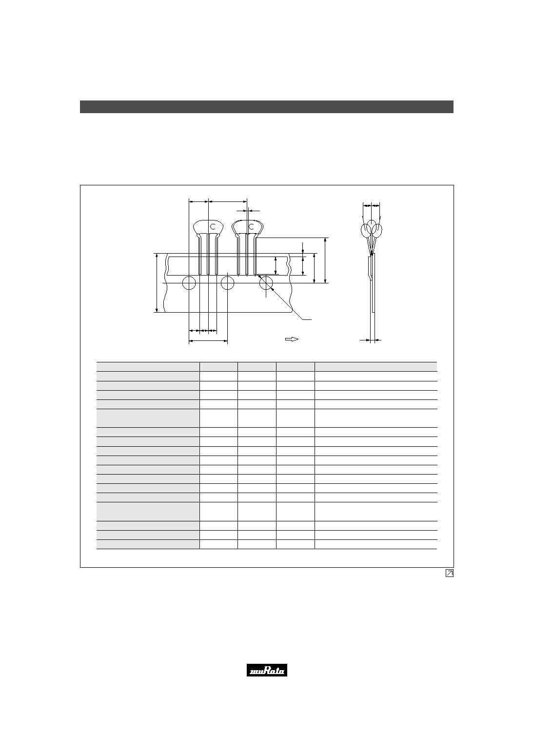
Please read CAUTION and Notice in this catalog for safety. This catalog has only typical specifications. Therefore you are requested
to approve our product specification or to transact the approval sheet for product specification, before your ordering.
P25E3.pdf 01.10.17
Lead Type Packaging
40
14
s Lead Type Minimum Quantity
Bulk : 500 pcs.
Ammo Pack : 2000 pcs. (SFSRA/TPSRA series)
1500 pcs. (CDSRH/TPWRD/TPTRD series)
s SFSRA/TPSRA Series
(in mm)
Lead length under the hole down tape
Pitch of component
Pitch of sprocket hole (I)
Length from hole center to lead
Length from hole center to
component center
Lead spacing (I)
Lead spacing (II)
Slant to the forward or backward
Slant to the left or right
Width of carrier tape
Width of hold down tape
Position of Sprocket hole
Gap of hold down tape and carrier Tape
Distance between the center of
sprocket hole and lead stopper
Diameter of sprocket hole
Total tape thickness
Pitch of sprocket hole (II)
Item
Code
Dimensions
Tolerance
Remarks
L
1
P
P
0
P
1
P
2
F
1
F
2
h
S
W
W
0
W
1
W
2
H
0
D
0
t
P
0
20
5.0 min.
12.7
12.7
3.85
6.35
2.5
2.5
0
0
18.0
6.0 min.
9.0
0
18.0
¯4.0
0.6
254.0
±
0.5
±
0.2
±
0.5
±
0.5
±
0.2
±
0.2
±
1.0
±
1.0
±
0.5
±
0.5
±
0.5
±
0.2
±
0.2
±
1.5
Tolerance for Pitches 10
Z
P
0
=127
±
1
Hold down tape doesn't exceed the carrier tape.
The pitch of 20 sprocket holes
M
M
P
2
P
S
W
H
0
W
1
W
0
L
1
W
2
D
0
t
P
0
P
1
F
1
F
2
Direction Feed
h
h
+0.5
≠0
Continued on the following page.

Please read CAUTION and Notice in this catalog for safety. This catalog has only typical specifications. Therefore you are requested
to approve our product specification or to transact the approval sheet for product specification, before your ordering.
P25E3.pdf 01.10.17
Lead Type Packaging
41
14
Continued from the preceding page.
s TPSRD/CDSRH_EK Series
(in mm)
Hold down tape doesn't exceed the carrier tape
The pitch of 20 sprocket holes
P
2
P
P
1
P
0
F
W
L
1
W
0
W
1
H
0
W
2
D
0
t
S
1
Item
Code
Dimensions
Tolerance
Remarks
Lead length under the hole down tape
Pitch of component
Pitch of sprocket hole (1)
Length from hole center to lead
Length from hole center to component center
Lead spacing
Slant to the forward or backward
Slant to the left or right
Width of carrier tape
Width of hold down tape
Position of sprocket hole
Diameter of sprocket hole
Total tape thickness
Pitch of sprocket hole (2)
L
1
P
P
0
P
1
P
2
F
h
S
1
W
W
0
W
1
W
2
H
0
D
0
t
Po20
3.0 min.
12.7
12.7
3.85
6.35
5.0
0
0
18.0
6.0 min.
9.0
0
18.0
¯4.0
0.6
254.0
------
±
0.5
±
0.2
±
0.5
±
0.5
±
1.0
±
1.0
±
0.5
------
±
0.5
±
0.5
±
0.2
±
0.2
±
1.5
+0.5
-0.0
+0.5
-0.2
h
h
Gap of hold down tape and
Carrier tape
Distance between the center of
sprocket hole and lead stopper
Continued on the following page.

Please read CAUTION and Notice in this catalog for safety. This catalog has only typical specifications. Therefore you are requested
to approve our product specification or to transact the approval sheet for product specification, before your ordering.
P25E3.pdf 01.10.17
Lead Type Packaging
42
14
Continued from the preceding page.
s TPSRD_W/TPWRD/TPTRD/CDSRH_CK Series
(in mm)
Lead Length under the Hold Down Tape
Length of Cat off
Pitch of Components
Pitch of Sprocket Hole (1)
Length from Hole Center to Lead
Length from Hole Center to Component Center
Pitch of the Terminal (1)
Pitch of the Terminal (2)
Slant to the Forward or Backward
Slant to the Left or Right
Width of Carrier Tape
Width of Hold Down Tape
Position of Sprocket Hole
Gap of Hold Down Tape and Carrier Tape
Distance Between the Center of Sprocket
Hole and Lead Stpper
Diameter of Sprocket Hole
Total Tape Thickness
Pitch of Sprocket Hole (2)
Item
Code
Dimensions
Tolerance
Remarks
L
1
L
2
P
P
0
P
1
P
2
F
F
1
h
S
1
W
W
0
W
1
W
2
H
0
D
0
t
P
0
20
3.0 min.
2.0 max.
12.7
12.7
3.85
6.35
5.0
2.5
0
0
18.0
6.0 min.
9.0
0
18.0
¯4.0
0.6
254.0
To distinguish the direction
Must not protrude to the carrier tape
The pitch of 20 sprocket holes
±
0.5
±
0.2
±
0.5
±
0.5
±
0.2
±
1.0
±
1.0
±
0.5
±
0.5
±
0.5
±
0.2
±
0.2
±
1.5
+0.5
≠0.2
+0.5
≠0
P
2
P
P
1
P
0
F
F
1
F
1
W
L
1
L
2
W
0
W
1
H
0
W
2
D
0
t
S
1
h
h

Head Office
2-26-10, Tenjin Nagaokakyo-shi, Kyoto 617-8555, Japan Phone:81-75-951-9111
International Division
3-29-12, Shibuya, Shibuya-ku, Tokyo 150-0002, Japan
Phone:81-3-5469-6123 Fax:81-3-5469-6155 E-mail:intl@murata.co.jp
http://www.murata.co.jp/products/
Please read CAUTION and Notice in this catalog for safety. This catalog has only typical specifications. Therefore you are requested
to approve our product specification or to transact the approval sheet for product specification, before your ordering.
P25E3.pdf 01.10.17
Note:
1. Export Control
<
For customers outside Japan
>
Murata products should not be used or sold for use in the development, production, stockpiling or utilization of any conventional weapons or mass-destructive
weapons (nuclear weapons, chemical or biological weapons, or missiles), or any other weapons.
<
For customers in Japan
>
For products which are controlled items subject to the "Foreign Exchange and Foreign Trade Law" of Japan, the export license specified by the law is required
for export.
2. Please contact our sales representatives or product engineers before using our products listed in this catalog for the applications listed below which require
especially high reliability for the prevention of defects which might directly cause damage to the third party's life, body or property, or when intending to use one
of our products for other applications than specified in this catalog.
q
Aircraft equipment
w
Aerospace equipment
e
Undersea equipment
r
Power plant equipment
t
Medical equipment
y
Transportation equipment (vehicles, trains, ships, etc.)
u
Traffic signal equipment
i
Disaster prevention / crime prevention equipment
o
Data-processing equipment
!0
Application of similar complexity and/or reliability requirements to the applications listed in the above
3. Product specifications in this catalog are as of September 2001. They are subject to change or our products in it may be discontinued without advance notice.
Please check with our sales representatives or product engineers before your ordering. If there are any questions, please contact our sales representatives or
product engineers.
4. Please read CAUTION and Notice in this catalog for safety. This catalog has only typical specifications. Therefore you are requested to approve our product
specification or to transact the approval sheet for product specification, before your ordering.
5. Please note that unless otherwise specified, we shall assume no responsibility whatsoever for any conflict or dispute that may occur in connection with the effect
of our and/or third party's intellectual property rights and other related rights in consideration of your using our products and/or information described or
contained in our catalogs. In this connection, no representation shall be made to the effect that any third parties are authorized to use the rights mentioned
above under licenses without our consent.
6. None of ozone depleting substances (ODS) under the Montreal Protocol is used in manufacturing process of us.