 | –≠–ª–µ–∫—Ç—Ä–æ–Ω–Ω—ã–π –∫–æ–º–ø–æ–Ω–µ–Ω—Ç: MU9C4480B | –°–∫–∞—á–∞—Ç—å:  PDF PDF  ZIP ZIP |
Document Outline
- Application Benefits
- Distinctive Characteristics
- General Description
- Operational Overview
- Pin Descriptions
- /E (Chip Enable, Input, TTL)
- /W (Write Enable, Input, TTL)
- /CM (Data/Command Select, Input, TTL)
- /EC (Enable Daisy Chain, Input, TTL)
- DQ15Ö0 (Data Bus, I/O, TTL)
- /MF (Match Flag, Output, TTL)
- /MI (Match Input, Input, TTL)
- /MA (Device Match Flag, Output, TTL)
- /MM (Device Multiple Match Flag, Output, TTL)
- /FF (Full Flag, Output, TTL)
- /FI (Full Input, Input, TTL)
- /RESET (Reset, Input, TTL)
- TEST1, TEST2 (Test, Input, TTL)
- VCC, GND (Positive Power Supply, Ground)
- Functional Description
- Operational Characteristics
- Instruction Set Descriptions
- Instruction Set Summary
- Register Bit Assignments
- Electrical
- Switching
- Timing Diagrams
- Dual Footprint Connections
- Packages
- Ordering Information
Data Sheet Draft
MUSIC Semiconductors, the MUSIC logo, and the phrase "MUSIC Semiconductors" are
October 20, 2000 Rev. 1
Registered trademarks of MUSIC Semiconductors. MUSIC is a trademark of
MUSIC Semiconductors.
APPLICATION BENEFITS
∑
New low-cost LANCAM family in a space-saving
TQFP package
∑
Fast speed allows processing of both DA and SA
within 450 ns, equivalent to 138 ports of 10 Base-T or
13 ports of 100 Base-T Ethernet
∑
Full CAM features allow all operations to be masked
on a bit-by-bit basis
∑
Powerful, LANCAM A/L compatible instruction set
for any list processing need
∑
Shiftable Comparand and Mask registers assist in
proximate matching algorithms
∑
Cascadable to any practical length with no
performance penalties
∑
Industrial temperature grades for harsh environments
∑
Dual footprint connections to conserve board space
∑
3.3 Volt for lower power systems
DISTINCTIVE CHARACTERISTICS
∑
High density CMOS Content Addressable Memory
(CAM)
∑
1K (1480B), 4K (4480B), 8K (8480B) words
∑
64-bit per word memory organization
∑
16-bit I/O
∑
Fast 50 ns compare speed
∑
Dual configuration register set for rapid context
switching
∑
16-bit CAM/RAM segments with MUSIC's patented
partitioning
∑
/MA and /MM output flags to enable faster system
performance
∑
Readable Device ID
∑
Selectable faster operating mode with no wait states
after a no-match
∑
Validity bit setting accessible from the Status register
∑
Single cycle reset for Segment Control register
∑
44- and 64-pin TQFP package
∑
3.3 Volt operation
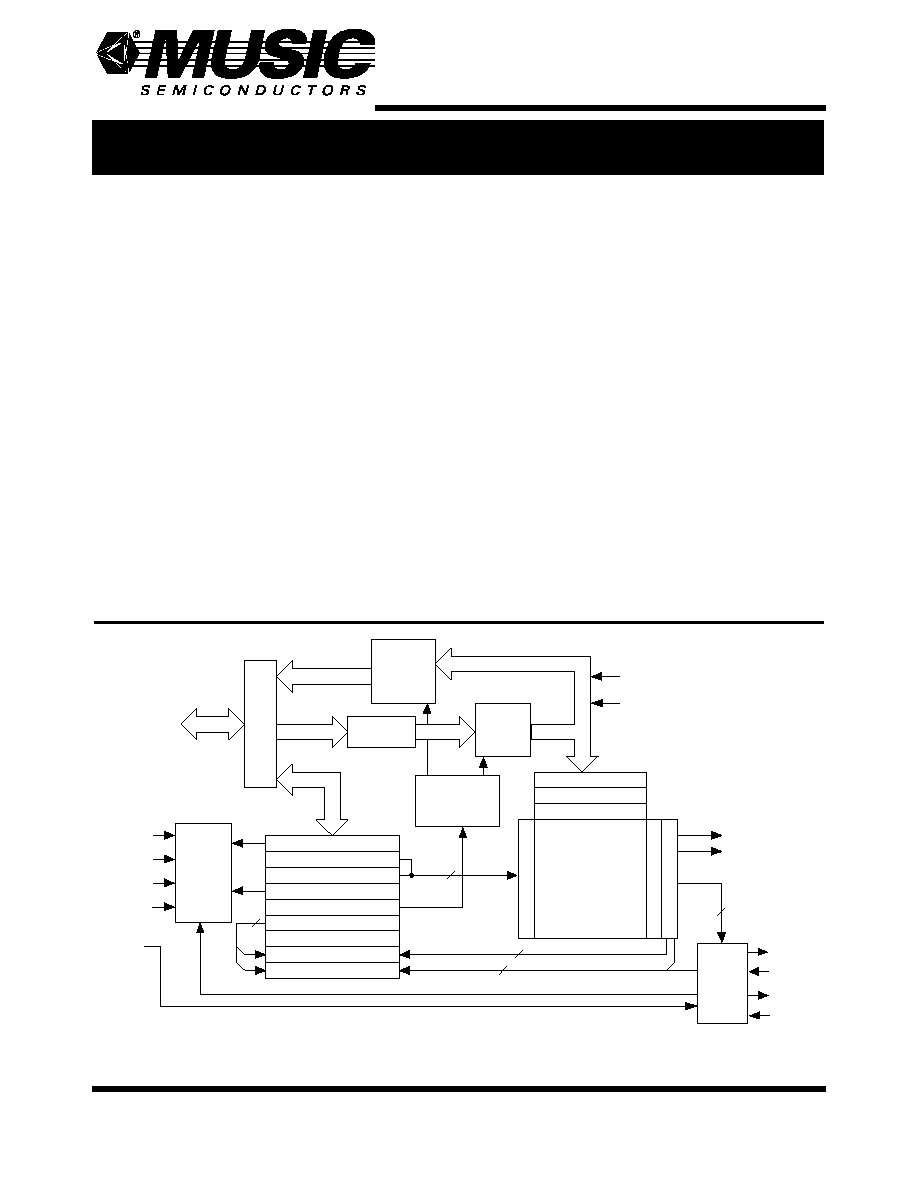
Figure 1: LANCAM B Family Block Diagram
/EC
DQ (15--0)
(16)
CAM ARRA Y
2
N
WORDS
X 64 BITS
COMPARAND*
MASK 1
MASK 2
2
N
X 2 VALIDITY BITS
PRIORITY ENCODER
COMMANDS & STATUS
2
N
DATA (16)
TRANSLATE
802 .3/80 2.5
DATA (16)
DEMUX
NEXT FREE ADDRESS (R/O)
CONTROL
SEGMENT CONTROL
PAGE ADDRESS (LOCAL )
DEVICE SELECT (GLOBAL)
ADDRESS
STATUS (31-16) (R/O)
REGISTER SET
2
MATCH ADDR
& /MA F LAG
/MM, /FL
DATA (16)
(16)
DATA (64)
DATA (64)
ADDRESS DECODER
/MA
/MM
N+1
16
I/O BUFFERS
CONTROL
SOURCE AND
DESTINATION
SEGMENT
COUNTERS
MUX
VCC
GND
/FF
/FI
/MF
/MI
MATCH
AND
FLAG
LOGIC
/W
/E
/CM
/RESET
INSTRUCTION (W/O)*
STATUS (15-0) ( R/O)*
LANCAM B Family
LANCAM B Family
LANCAM B Family
LANCAM B Family

LANCAM B Family
General Description
2
Rev. 1
GENERAL DESCRIPTION
The LANCAM consists of various depths of 64-bit
Content Addressable Memories (CAMs), with a 16-bit
wide interface.
CAMs, also known as associative memories, operate in the
converse way to random access memories (RAM). In
RAM, the input to the device is an address and the output
is the data stored at that address. In CAM, the input is a
data sample and the output is a flag to indicate a match and
the address of the matching data. As a result, CAM
searches large databases for matching data in a short,
constant time period, no matter how many entries are in
the database. The ability to search data words up to 64 bits
wide allows large address spaces to be searched rapidly
and efficiently. A patented architecture links each CAM
entry to associated data and makes this data available for
use after a successful compare operation.
The MUSIC LANCAMs are ideal for address filtering and
translation applications in LAN switches and routers. The
LANCAMs are also well suited to encryption, database
accelerators, and image processing.
OPERATIONAL OVERVIEW
To use the LANCAM, the user loads the data into the
Comparand register, which is automatically compared to
all valid CAM locations. The device then indicates
whether or not one or more of the valid CAM locations
contains data that matches the target data. The status of
each CAM location is determined by two validity bits at
each memory location. The two bits are encoded to render
four validity conditions: Valid, Empty, Skip, and RAM,
shown in Status Register Bits on page 24 (bits 29:28). The
memory can be partitioned into CAM and associated
RAM segments on 16-bit boundaries, but by using one of
the two available Mask registers, the CAM/RAM
partitioning can be set at any arbitrary size between zero
and 64 bits.
The LANCAM's internal data path is 64 bits wide for
rapid internal comparison and data movement. Vertical
cascading of additional LANCAMs in a daisy chain
fashion extends the CAM memory depth for large
databases. Cascading requires no external logic. Loading
data to the Control, Comparand, and Mask registers
automatically triggers a compare. Compares also may be
initiated by a command to the device. Associated RAM
data is available immediately after a successful compare
operation. The Status register reports the results of
compares including all flags and addresses. Two Mask
registers are available and can be used in two different
ways: to mask comparisons or to mask data writes. The
RAM validity type allows additional masks to be stored in
the CAM array where they may be retrieved rapidly.
A simple four-wire control interface and commands
loaded into the Instruction decoder control the device. A
powerful instruction set increases the control flexibility
and minimizes software overhead. Additionally, dedicated
pins for match and multiple-match flags enhance
performance when the device is controlled by a state
machine. These and other features make the LANCAM a
powerful associative memory that drastically reduces
search delays.

Pin Descriptions
LANCAM B Family
Rev. 1
3
PIN DESCRIPTIONS
Note: All signals are implemented in CMOS technology with TTL levels. Signal names that start with a slash ("/") are active LOW.
Inputs should never be left floating. The CAM architecture draws large currents during compare operations, mandating the use of good
layout and bypassing techniques. Refer to the DC Electrical Characteristics on page 25 for more information.
Figure 2: 44-Pin TQFP
Figure 3: 64-Pin TQFP
/E (Chip Enable, Input, TTL)
The /E input enables the device while LOW. The falling
edge registers the control signals /W, /CM, and /EC. The
rising edge locks the daisy chain, turns off the DQ pins,
and clocks the Destination and Source Segment counters.
The four cycle types enabled by /E are shown in Table 1.
/W (Write Enable, Input, TTL)
The /W input selects the direction of data flow during a
device cycle. /W LOW selects a Write cycle and /W HIGH
selects a Read cycle.
/CM (Data/Command Select, Input, TTL)
The /CM input selects whether the input signals on
DQ15≠0 are data or commands. /CM LOW selects
Command cycles and /CM HIGH selects Data cycles.
/EC (Enable Daisy Chain, Input, TTL)
The /EC signal performs two functions. The /EC input
enables the /MF output to show the results of a
comparison, as shown in Figure 9 on page 14. If /EC is
LOW at the falling edge of /E in a given cycle, the /MF
output is enabled. Otherwise, the /MF output is held
HIGH.
The /EC signal also enables the /MF≠/MI daisy chain,
which serves to select the device with the highest-priority
match in a string of LANCAMs. Table 4 explains the
effect of the /EC signal on a device with or without a
match in both Standard and Enhanced modes. /EC must be
HIGH during initialization.
DQ15≠0 (Data Bus, I/O, TTL)
The DQ15≠0 lines convey data, commands, and status to
and from the LANCAM. /W and /CM control the direction
and nature of the information that flows to or from the
device. When /E is HIGH, DQ15≠0 go to HIGH-Z.
/MF (Match Flag, Output, TTL)
The /MF output goes LOW when one or more valid
matches occur during a compare cycle. /MF becomes valid
after /E goes HIGH on the cycle that enables the daisy
chain (on the first cycle that /EC is registered LOW by the
previous falling edge of /E; see Figure 9 on page 14). In a
daisy chain, valid match(es) in higher priority devices are
passed from the /MI input to /MF. If the daisy chain is
enabled but the match flag is disabled in the Control
register, the /MF output only depends on the /MI input of
the device (/MF=/MI). /MF is HIGH if there is no match
or when the daisy chain is disabled (/E goes HIGH when
/EC was HIGH on the previous falling edge of /E). The
System Match flag is the /MF pin of the last device in the
daisy chain. /MF is reset when the active configuration
register set is changed.
44-Pin TQFP
(Top View)
/MM
/FF
/FI
/CM
/EC
GND
DQ0
DQ1
DQ2
DQ3
VCC
GND
DQ4
DQ5
VCC
VCC
TEST2
GND
GND
DQ6
DQ7
VCC
GND
DQ15
DQ14
DQ13
DQ12
GND
DQ11
DQ10
DQ9
DQ8
GND
/MA
/MI
/MF
GND
/RESET
VCC
VCC
TEST1
/E
/W
GND
22
21
20
19
18
17
16
15
14
13
12
33
32
31
30
29
28
27
26
25
24
23
1
2
3
4
5
6
7
8
9
10
11
34
35
36
37
38
39
40
41
42
43
44
DQ15
DQ14
DQ13
DQ12
16
15
14
13
12
1
2
3
4
5
6
7
8
9
10
11
22
21
20
19
18
17
24
23
28
27
26
25
32
31
30
29
37
38
39
40
41
42
43
44
33
34
35
36
45
46
47
48
58
59
60
61
62
63
56
57
52
53
54
55
49
50
64
51
NC
DQ4
DQ5
VCC
VCC
TEST2
GND
GND
DQ6
DQ7
VCC
NC
GND
GND
GND
NC
GND
GND
DQ11
DQ10
DQ9
DQ8
GND
NC
GND
GND
GND
NC
/MA
/MI
/MF
GND
/RESET
VCC
VCC
TEST1
/E
/W
GND
NC
NC
GND
GND
NC
64-Pin TQFP
(Top View)
/MM
/FF
/FI
/CM
/EC
GND
DQ0
DQ1
DQ2
DQ3
VCC
NC
NC
GND
NC
NC
Table 1: I/O Cycles
/W
/CM
Cycle Type
LOW
LOW
Command Write Cycle
LOW
HIGH
Data Write Cycle
HIGH
LOW
Command Read Cycle
HIGH
HIGH
Data Read Cycle

LANCAM B Family
Pin Descriptions
4
Rev. 1
/MI (Match Input, Input, TTL)
The /MI input prioritizes devices in vertically cascaded
systems. It is connected to the /MF output of the previous
device in the daisy chain. The /MI pin on the first device in
the chain must be tied HIGH.
/MA (Device Match Flag, Output, TTL)
The /MA output is LOW when one or more valid matches
occur during the current or the last previous compare
cycle. The /MA output is not qualified by /EC or /MI, and
reflects the match flag from that specific device's Status
register. /MA is reset when the active register set is
changed.
/MM (Device Multiple Match Flag, Output, TTL)
The /MM output is LOW when more than one valid match
occurs during the current or the last previous compare
cycle. The /MM output is not qualified by /EC or /MI, and
reflects the multiple match flag from that specific device's
Status register. /MM is reset when the active register set is
changed.
/FF (Full Flag, Output, TTL)
If enabled in the Control register, the /FF output goes
LOW when no empty memory locations exist within the
device (and in the daisy chain above the device as
indicated by the /FI pin). The System Full flag is the /FF
pin of the last device in the daisy chain, and the Next Free
address resides in the device with /FI LOW and /FF
HIGH. If disabled in the Control register, the /FF output
only depends on the /FI input (/FF = /FI).
/FI (Full Input, Input, TTL)
The /FI input generates a CAM-Memory-System-Full
indication in vertically cascaded systems. It is connected
to the /FF output of the previous device in the daisy chain.
The /FI pin on the first device in a chain must be tied
LOW.
/RESET (Reset, Input, TTL)
/RESET must be driven LOW to place the device in a
known state before operation, which resets the device to
the conditions shown in Table 3 on page 11. The /RESET
pin should be driven by TTL levels, not directly by an RC
timeout. /E must be kept HIGH during /RESET.
TEST1, TEST2 (Test, Input, TTL)
These pins enable MUSIC production test modes that are
not usable in an application. They should be connected to
ground, either directly or through a pull-down resistor, or
they may be left unconnected. These pins may not be
implemented on all versions of these products.
VCC, GND (Positive Power Supply, Ground)
These pins are the power supply connections to the
LANCAM. VCC must meet the voltage supply
requirements in the Operating Conditions section relative
to the GND pins, which are at 0 volts (system reference
potential), for correct operation of the device. All the
ground and power pins must be connected to their
respective planes with adequate bulk and high frequency
bypassing capacitors in close proximity to the device.

Functional Description
LANCAM B Family
Rev. 1
5
FUNCTIONAL DESCRIPTION
The LANCAM is a Content Addressable Memory (CAM)
with 16-bit I/O for network address filtering and
translation, virtual memory, data compression, caching,
and table lookup applications. The memory consists of
static CAM, organized in 64-bit data fields. Each data field
can be partitioned into a CAM and a RAM subfield on
16-bit boundaries. The contents of the memory can be
randomly accessed or associatively accessed by the use of
a compare. During automatic comparison cycles, data in
the Comparand register is automatically compared with
the "Valid" entries in the memory array. The Device ID
can be read using a TCO PS instruction (see Persistent
Source Register Bits on page 24).
Data Input and Output Characteristics
The data inputs and outputs of the LANCAM are
multiplexed for data and instructions over a 16-bit I/O bus.
Internally, data is handled on a 64-bit basis, since the
Comparand register, the Mask registers, and each memory
entry are 64 bits wide. Memory entries are globally
configurable into CAM and RAM segments on 16-bit
boundaries, as described in US Patent 5,383,146 assigned
to MUSIC Semiconductors. Seven different CAM/RAM
splits are possible, with the CAM width going from one to
four segments, and the remaining RAM width going from
three to zero segments. Finer resolution on compare width
is possible by invoking a Mask register during a compare,
which allows global masking on a bit basis. The CAM
subfield contains the associative data, which enters into
compares, while the RAM subfield contains the associated
data, which is not compared. In LAN bridges, the RAM
subfield could hold, for example, port-address and aging
information related to the destination or source address
information held in the CAM subfield of a given location.
In a translation application, the CAM field could hold the
dictionary entries, while the RAM field holds the
translations, with almost instantaneous response.
Validity Bits
Each entry has two validity bits associated with it to define
its particular type: Empty, Valid, Skip, or RAM. When
data is written to the active Comparand register, and the
active Segment Control register reaches its terminal count,
the contents of the Comparand register are automatically
compared with the CAM portion of all the valid entries in
the memory array. For added versatility, the Comparand
register can be barrel-shifted right or left one bit at a time.
A Compare instruction then can be used to force another
compare between the Comparand register and the CAM
portion of memory entries of any one of the four validity
types. After a Read or Move from Memory operation, the
validity bits of the location read or moved are copied into
the Status register, where they can be read using
Command Read cycles.
Data Movement (Read/Write)
Data can be moved from one of the data registers (CR,
MR1, or MR2) to a memory location that is based on the
results of the last comparison (Highest-Priority Match or
Next Free), or to an absolute address, or to the location
pointed to by the active Address register. Data can also be
written directly to the memory from the DQ bus using any
of the above addressing modes. The Address register may
be directly loaded and may be set to increment or
decrement, allowing DMA-type reading or writing from
memory.
Configuration Register Sets
Two sets of configuration registers (Control, Segment
Control, Address, Mask Register 1, and Persistent Source
and Destination) are provided to permit rapid context
switching between foreground and background activities.
The currently active set of configuration registers controls
writes, reads, moves, and compares. The foreground set
typically would be pre-loaded with values useful for
comparing input data, often called filtering, while the
background set would be pre-loaded with values useful for
housekeeping activities such as purging old entries.
Moving from the foreground task of filtering to the
background task of purging can be done by issuing a
single instruction to change the current set of
configuration registers. The match condition of the device
is reset whenever the active register set is changed.
Control Register
The active Control register determines the operating
conditions within the device. Conditions set by this
register's contents are reset, enable or disable Match flag,
enable or disable Full flag, CAM/RAM partitioning,
disable or select masking conditions, disable or select
auto-incrementing or auto-decrementing the Address
register, and select Standard or Enhanced mode. The
active Segment Control register contains separate counters
to control the writing of 16-bit data segments to the
selected persistent destination, and to control the reading
of 16-bit data segments from the selected persistent
source.
Mask Registers
There are two active Mask registers at any one time, which
can be selected to mask comparisons or data writes. Mask
Register 1 has both a foreground and background mode to
support rapid context switching. Mask Register 2 does not
have this mode, but can be shifted left or right one bit at a
time. For masking comparisons, data stored in the active
selected Mask register determines which bits of the
comparand are compared against the valid contents of the
memory. If a bit is set HIGH in the Mask register, the same
bit position in the Comparand register becomes a "don't