 | –≠–ª–µ–∫—Ç—Ä–æ–Ω–Ω—ã–π –∫–æ–º–ø–æ–Ω–µ–Ω—Ç: CS5852 | –°–∫–∞—á–∞—Ç—å:  PDF PDF  ZIP ZIP |
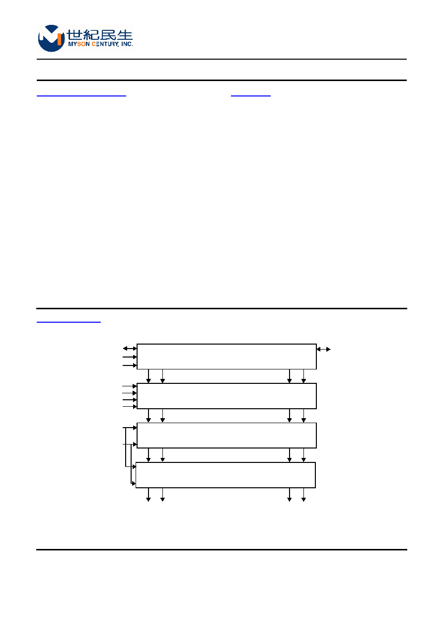
BLOCK DIAGRAM
GENERAL DESCRIPTION
FEATURES
CS5852
TFT Gate Driver (256 Outputs)
USA:
4020 Moorpark Avenue Suite 115
San Jose, CA, 95117
Tel: 408-243-8388 Fax: 408-243-3188
Sales@myson.com.tw
www.myson.com.tw
Rev. 1.0 January 2003
page 1 of 11
Myson Century, Inc.
Taiwan:
No. 2, Industry East Rd. III,
Science-Based Industrial Park, Hsin-Chu, Taiwan
Tel: 886-3-5784866 Fax: 886-3-5784349
The CS5852 is a TFT LCD gate driver with 256
outputs for XGA/SXGA display systems. The logic
and control portion is implemented in standard
CMOS circuits while the output drivers use high
voltage CMOS design. The low voltage part includes
a 256-stage bidirectional shift register with right and
left shift I/O for cascading. The output of the shift
register is then level translated to drive the high
voltage output buffer. There are four supply voltages
for the CS5852. VDD/VLL are the supply voltages for
logic interfaces. Typically VDD is at 3.3V while VLL is
0V. VGON and VSS are the supply voltages for the
output driver. VSS is the most negative supply
voltage for the internal substrate of the CS5852.
The CS5852 allows three output enable controls
(OE1-3) and one global enable signal (XON).
∑ 256 gate drive outputs
∑ Bidirectional shift control and cascadable
∑ Output enable and global on control
∑ Maximum shift clock frequency up to 100KHz
∑ 3.3V CMOS logic I/O
∑ High voltage output drive
∑ Operating supply range
Logic (VDD-VLL: 3.3V)
Output Drive (VGON -VSS: 40V)
∑ TCP package
DIOL
SCLK
SHIFT CONTROL REGISTER
CS5852
ENABLE CONTROL
OUTPUT BUFFER
LEVEL SHIFT
DIOR
RL
OE1,2,3
XON
VGON
OUT1 OUT2
OUT255 OUT256
VDD
VLL
VSS
CS5852
page 2 of 11
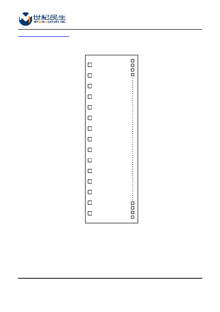
PIN CONNECTION DIAGRAM
Figure-1
IC top view. This diagram shows CS5852's pin configuration only. The VAA and RESETN pins
are used for internal tests and are not shown in the pad layout. Usage of these two pins is not
compulsory.
VSS
VSS
VLL
DIOL
RL
SCLK
XON
OE1
OE2
OE3
DIOR
VDD
VGON
VAA
RESETN
OUT1
OUT2
OUT3
OUT4
OUT253
OUT254
OUT255
OUT256
CS5852
CS5852
page 3 of 11
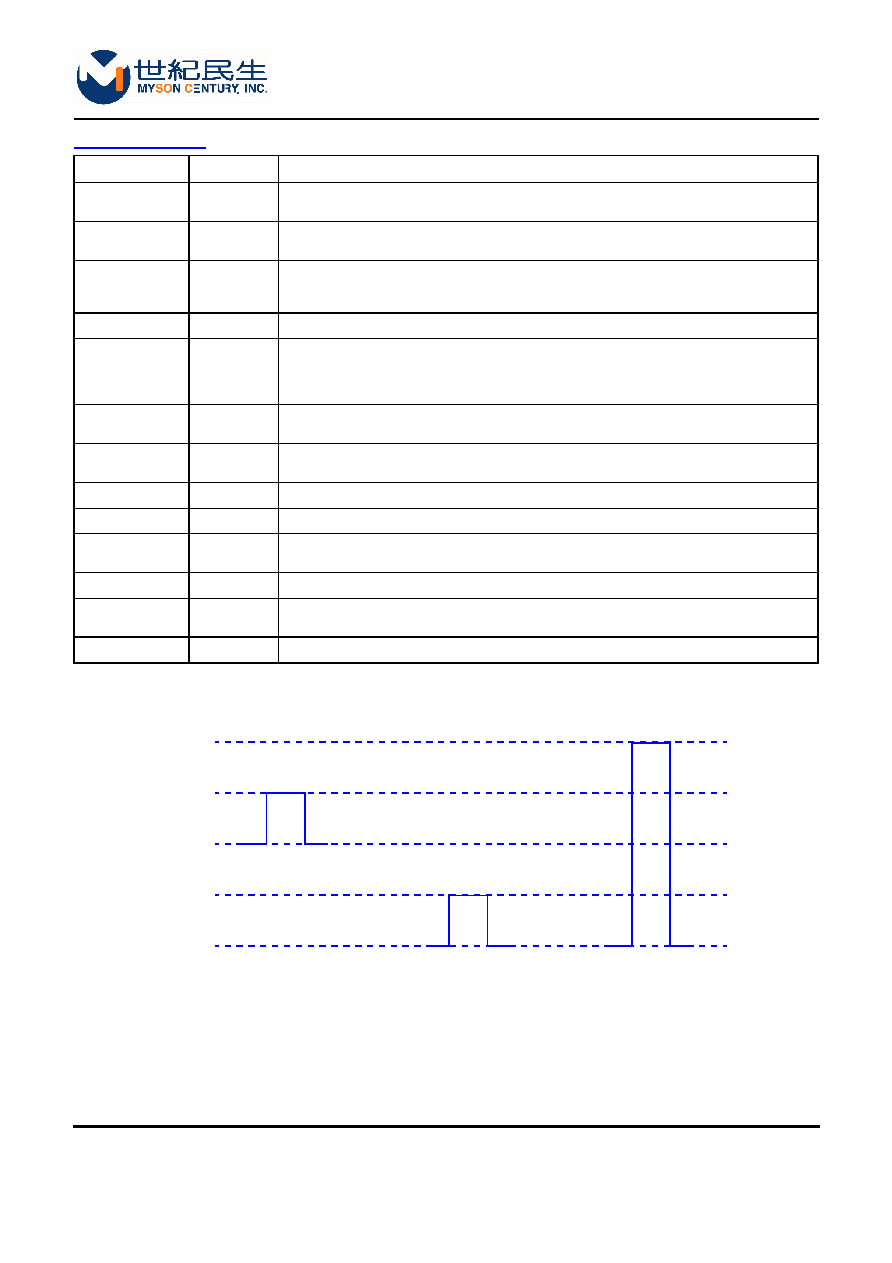
PIN DESCRIPTION
Note: RESETN and VAA is not connected to the TCP package.
Figure-2
Name Pin
Description
SCLK
I
Shift clock. This is a 3.3V CMOS level input for shift register clock. The rising edge of
SCLK is used.
RL
I
Right/Left shift control. RL=1 is shift right (OUT1 -> OUT256), RL=0 is shift left (OUT256
-> OUT1).
DIOR
I/O
Right Data I/O. This is a bidirectional shift data for the right side. It is an output when
RL=1, and an input when RL=0. DIOR and DIOL are used to cascade multiple CS5852s
to form more than 256 outputs.
DIOL
I/O
Left Data I/O. This is the bidirectional shift data for the left side.
OE1,
OE2,
OE3
I
Output enable control. The output is forced low when OE is high.
OE1 controls output 1,4,...,253,256. The control is asynchronous to SCLK.
OE2 controls output 2,5,...,251,254. The control is asynchronous to SCLK.
OE3 controls output 3,6,...,252,255. The control is asynchronous to SCLK.
XON
I
Global on control. When XON=0, all outputs are forced high. XON is asychronous to
SCLK. Internal pulled high with a 50K
resistor.
OUT
[1-256]
O
Output drive. These are the gate drive outputs. The high level is VGON and the low level
is VSS.
VDD
P
Positive supply for the CMOS logic I/O. This is typically 3.3V.
VLL
P
Negative supply for the CMOS logic I/O. This is typically 0V.
VGON
P
Positive supply for the output driver. This is typically the most positive supply voltage to
CS5852.
VAA
P
Positive supply for the internal logic circuits.
VSS
P
Negative supply for the output drive and the substrate. This is the most negative supply
voltage to CS5852.
RESETN
I
Active low reset pin. This signal uses to reset internal shift registers.
VGON
VDD
VLL
VAA
VSS
Input
DIOR
DIOL
Internal logic
LCD drive output
CS5852
page 4 of 11
FUNCTIONAL DESCRIPTION
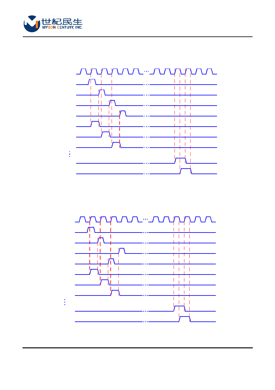
1. When RL is "HIGH" and a start pulse inputs the DIOL pin, this pulse is shifted right by the shift control register
at the rising edge of SCLK. While the output of the shift control register is "HIGH", the OUTn [n=1, 2, 3,..., 256]
is pulled to VGON. If the output of the shift control register is "LOW", OUTn [n=1, 2, 3,..., 256] is pushed to
VSS; DIOR is pulled to high at the falling edge of the 256th clock of SCLK and is pushed to low at the falling
edge of the 257th clock of SCLK. Please refer to operating waveform (1).
2. When RL is "LOW" and a start pulse inputs the DIOR pin, this pulse is shifted left by the shift control register at
the rising edge of SCLK. While the output of the shift control register is "HIGH", the OUTn [n=256, 255, 254,...,
1] is pulled to VGON. If the output of the shift control register is "LOW", OUTn [n=256, 255, 254,..., 1] is
pushed to VSS; DIOL is pulled to high at the falling edge of the 256th clock of SCLK and is pushed to low at
the
falling edge of the 257th clock of SCLK. Please refer to operating waveform (2).
3. OE1, OE2, and OE3 can disable OUTn [n=1, 2, 3,..., 256]. They are asynchronous to SCLK.
OUTn [n=1, 4, 7,..., 253, 256] is pushed to VSS when OE1 is "HIGH".
OUTn [n=2, 5, 8,..., 251, 254] is pushed to VSS when OE2 is "HIGH".
OUTn [n=3, 6, 9,..., 252, 255] is pushed to VSS when OE3 is "HIGH".
Please refer to operating waveform (1) and (2).
4. The global on control XON can enable OUTn [n=1, 2, 3,..., 256]. It is asynchronous to SCLK. Whenever XON
is "LOW", all outputs of CS5852 are pulled to VGON at the same time. Please refer to operating waveform (3).
CS5852
page 5 of 11
TIMING DIAGRAM
Figure-3 Operating Waveforms (1)
Figure-4 Operating Waveforms (2)
1
2
SCLK
DIOL
OE1
3
4
5
254
255
OE2
DIOR
OUT1
OE3
256
257
OUT2
OUT3
OUT256
RL=1, shift right
1
2
SCLK
DIOR
OE1
3
4
5
254
255
OE2
DIOL
OUT256
OE3
256
257
OUT255
OUT254
OUT1
RL=0, shift left