 | –≠–ª–µ–∫—Ç—Ä–æ–Ω–Ω—ã–π –∫–æ–º–ø–æ–Ω–µ–Ω—Ç: CS6707 | –°–∫–∞—á–∞—Ç—å:  PDF PDF  ZIP ZIP |
CS6707
200Mbps Fiber-Optic LED Driver
USA:
4020 Moorpark Avenue Suite 115
San Jose, CA, 95117
Tel: 408-243-8388 Fax: 408-243-3188
Sales@myson.com.tw
www.myson.com.tw
Rev.1.4 November 2002
page 1 of 13
Myson Century, Inc.
Taiwan:
No. 2, Industry East Rd. III,
Science-Based Industrial Park, Hsin-Chu, Taiwan
Tel: 886-3-5784866 Fax: 886-3-5784349
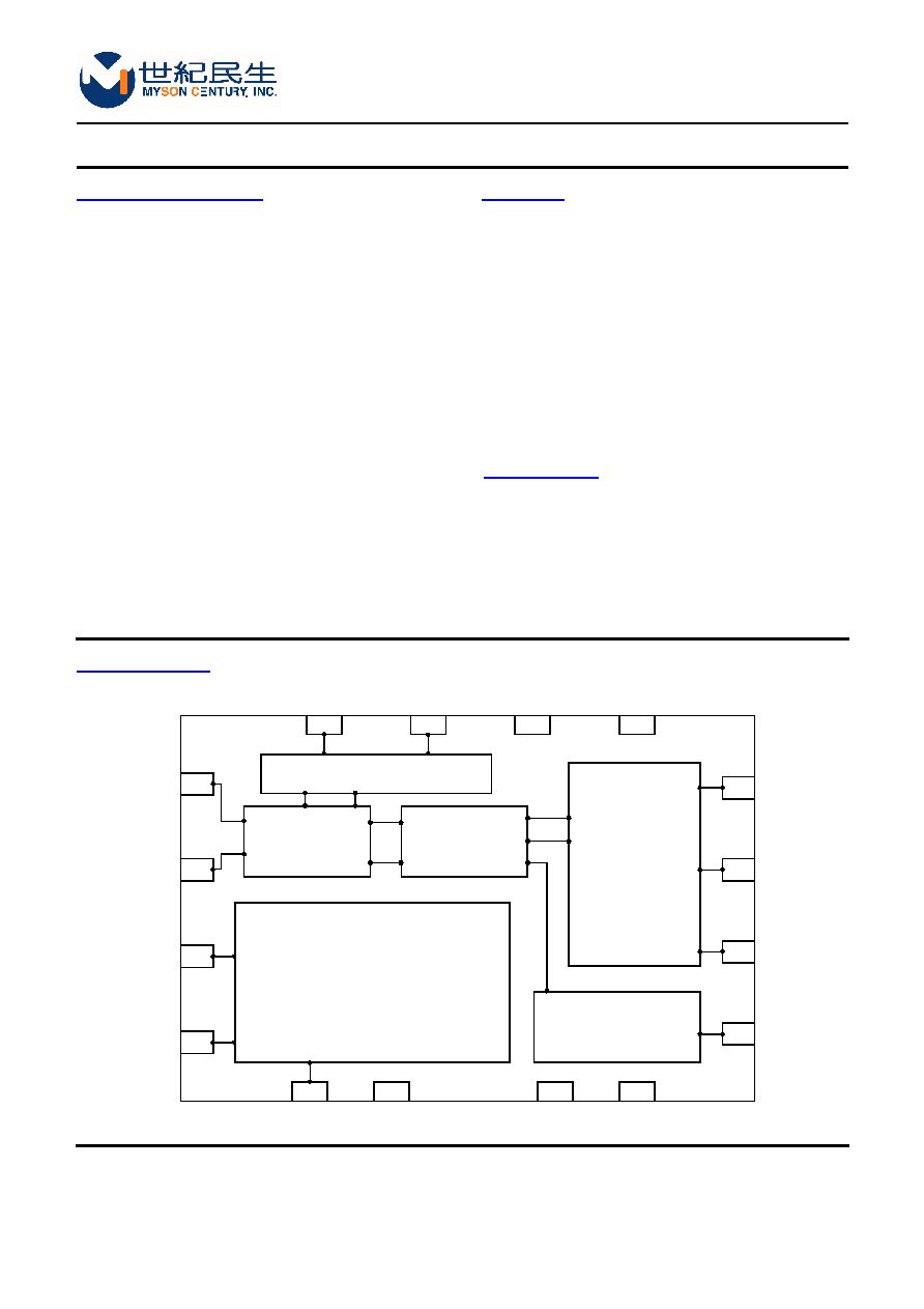
BLOCK DIAGRAM
GENERAL DESCRIPTION
FEATURES
APPLICATIONS
The CS6707 is a high-speed fiber optic LED driver
ideally suited for applications up to 200Mbps. The
CS6707 accepts differential PECL inputs which can
be shaped, if desired, by pins PWAI (Pulse Width
Adjust Increase) or PWAD (Pulse Width Adjust
Decrease).
Simply leave these two pins unconnected if no
adjustment is needed, then default mark/space ratio
is about 42/58. To improve LED "on and off" time, a
peaking and clamp circuit is included in the CS6707
which may be set via a RC network.
The temperature independent drive current of the
CS6707 can be set via an external resistor between
the RMOD pin and the ground. An external resistor
between pins RMOD and RMOD1 is used to
compensate the drive current for temperature
changes. Normally the CS6707 is direct coupled to
PECL inputs, however if AC coupling is desired, a 1/
3V
DD
bias point is recommended. Please refer to the
application circuit schematic for more details.
∑ Rise/fall time < 1ns, suited for applications up to
200Mbps.
∑ Maximum programmable 100mA LED drive
current.
∑ Maximum 2V LED forward voltage drop.
∑ Differential PECL inputs with optional pulse width
adjust feature.
∑ Temperature compensation of the LED driving
current.
∑ Supports both 3.3 and 5 Volt operation.
∑ Available as die or in QSOP-16/TSSOP-20
packages.
PULSE WIDTH ADJUSTMENT
ECL-CMOS
INVERTER BANK
BIAS CIRCUIT
PEAK CIRCUIT
CURRENT SWITCH
DINP
DINN
ROFS
RMOD1
RMOD
VDD1
VDD2
VDD3
PEAK
MODP
MODP
MODN
VSS2
VSS1
PWAD
PWAI
∑ FDDI
∑ SDH STM-1
∑ SONET OC-3
∑ Fiber Channel
∑ 100BaseF Ethernet
∑ LED Driver Transmitters

CS6707
page 2 of 13
DIE CONNECTION DIAGRAM
PIN CONNECTION DIAGRAM
DINN
MODP
MODP
RMOD1
PEAK
1.690 mm
1.550 mm
MODN
DINP
ROFS
PWAI
PWAD
GND
GND
RMOD
V
DD1
V
DD2
V
DD3
Figure-1
1
2
3
4
5
6
7
8
1
2
3
4
5
6
7
8
9
10
NC
GND
GND
MODN
MODP
MODP
PEAK
V
DD3
V
DD2
NC
NC
PWAD
PWAI
DINP
DINN
ROFS
RMOD1
RMOD
V
DD1
NC
20
19
18
17
16
15
14
13
12
11
GND
GND
MODN
MODP
MODP
PEAK
V
DD3
V
DD2
PWAD
PWAI
DINP
DINN
ROFS
RMOD1
RMOD
V
DD1
16
15
14
13
12
11
10
9
CS6707R
CS6707N
Figure-1 QSOP-16
Figure-2 TSSOP-20

CS6707
page 3 of 13
PIN DESCRIPTION
Name
Pin
QSOP-
16
Pin
TSSOP-
20
Die Pad
Description
PWAD
1
2
1
Pulse width adjustment decrease pin.
PWAI
2
3
2
Pulse width adjustment increase pin.
DINP
3
4
3
Differential data input pin. Complementary to DINN.
DINN
4
5
4
Inverse differential data input pin. Complementary to DINP.
ROFS
5
6
5
ECL to CMOS bias current set pin.
RMOD1
6
7
6
Temperature compensation adjustment pin.
RMOD
7
8
7
Temperature independent drive current set pin.
V
DD1
8
9
8
Analog power Pin. Connect to most positive supply voltage.
V
DD2
9
12
9
Digital power pin. Connect to most positive supply voltage.
V
DD3
10
13
10
LED pin. Connect to most positive supply voltage to speed `off' time of LED if
clamping circuit is not used.
PEAK
11
14
11
Connection for peaking circuit. Please refer to the application schematic.
MODP
12
15
12
Driver output pin. Connect LED between this pin and V
DD
.
MODP
13
16
13
Driver output pin. Connect LED between this pin and V
DD
.
MODN
14
17
14
Logical inverse of pins MODP. Connect a resistor of approximately the
same value as LED between this pin and V
DD
.
GND
15
18
15
Ground Pin. Connect to the most negative supply voltage.
GND
16
19
16
Ground Pin. Connect to the most negative supply voltage.
N.C.
1,10,
11,20
No connection.

CS6707
page 4 of 13
PRODUCT DESCRIPTION
The CS6707 consists of a modulation current drive with temperature compensation, the pulse width adjustment
circuit, the peaking and clamping circuit.
Modulation Current Drive With Temperature Compensation
A. Temperature Independent
The modulation current (Imod) can be set by connecting a resistor Rset bwtween the Rmod pin and the ground.
One can set Imod by choicing the unique Rset from the figure -4 or figure-5 depending on Vdd=3.3V or Vdd=5V.
The figure-4 and figure-5 show the relation between Imod and Rset independent of temperature compensation.
The approximation relation between Imod and Rset is
Vref is the voltage at the Rmod pin about 1.13V, K1 is 1100
±
100.
B. Temperature Dependent
If the temperature compensation of the LED current is desired. One can use the Table-1, Figure-6, Figure-4,
Figure-5 to implement the temperature compensation feature. The Table-1 and Figure-6 show the internal diode
threshold voltage (Vth) via the various R
TCM
value at different temperature, which R
TCM
is a resistor between the
Rmod pin and the Rmod1 pin. One can use the formula below to set the R
TCM
.
T2 and T1 are the different termperature, T2 >T1. Then use
to set the Rset value.
The pulse width adjustment
The pulse width of the LED ON/OFF time can be set with connecting the PWAI and PWAD pins to the ground by
a resistor Rpwai and Rpwad individually. If let Rpwad floating and Rpwai connect, the LED ON time will increase.
If let Rpwai floating and Rpwad connect, the LED ON time will decrease. Refer to the Fingure-7, Fingure-8,
Fingure-9 and Fingure-10 to get the Rpwai and Rpwad setting.
The peaking and clamping circuit
Generally. The turn-off time of the LED is longer than the turn-on time. One can use the clamping circuit to
improve this situation. The clamping feature can get by the V
DD3
pin connection. If the V
DD3
pin is floating, then
the clamping feature is off. The clamping circuit will delay the turn-on time of the LED. It becomes noticeable
when the LED driving current is low. One can connect a RC network between the MODP and PEAK pins to slove
this problem. See the application ciucuits to get the detail information.
Imod = K1 x
Vref
Rset
R
TCM
= K1 x
Vth (T1)
Imod (T2)
Vth (T2)
Imod (T1)
.
.
Imod (T1) = K1 x [ + ]
Vref
Rset
Vref - Vth (T1)
R
TCM

CS6707
page 5 of 13
TYPICAL OPERATING CURVE
Figure-4
Figure-5
Rset vs Imod simulated curve at Vdd=3.3V
0
10
20
30
40
50
60
70
80
90
100
15
28
41
54
67
80
93
106
119
132
145
158
171
184
197
210
223
236
249
262
275
288
301
314
327
340
353
366
379
392
Rset(k ohm)
Imod(mA)
Temp=25C
Rset vs Imod simulated curve at Vdd=5.0V
0
20
40
60
80
100
120
15 29 43 57 71 85 99 113 127 141 155 169 183 197 211 225 239 253 267 281 295 309 323 337 351 365 379 393
Rset(k ohm)
Imod(mA)
Temp=25C
∑
Both MODP and MODN pins connect a
20
resistor to Vdd.
∑
Rofs pin is floating.
∑
Both MODP and MODN pins connect a
20
resistor to Vdd.
∑
Rofs pin is floating.