 | –≠–ª–µ–∫—Ç—Ä–æ–Ω–Ω—ã–π –∫–æ–º–ø–æ–Ω–µ–Ω—Ç: MTD981 | –°–∫–∞—á–∞—Ç—å:  PDF PDF  ZIP ZIP |
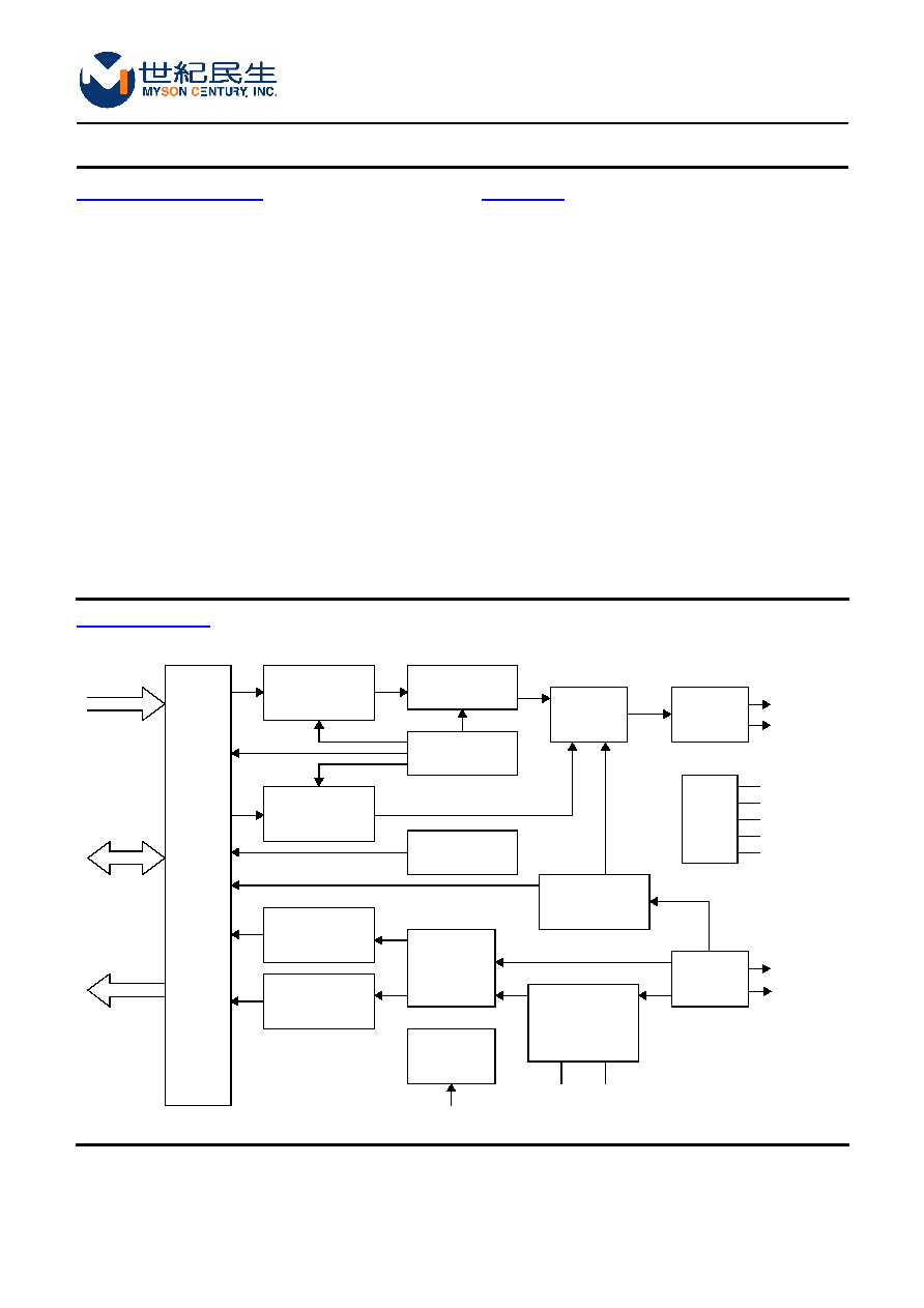
BLOCK DIAGRAM
GENERAL DESCRIPTION
FEATURES
MTD981
USA:
4020 Moorpark Avenue Suite 115
San Jose, CA, 95117
Tel: 408-243-8388 Fax: 408-243-3188
Sales@myson.com.tw
www.myson.com.tw
Rev. 1.4 February 2003
page 1 of 17
Myson Century, Inc.
Taiwan:
No. 2, Industry East Rd. III,
Science-Based Industrial Park, Hsin-Chu, Taiwan
Tel: 886-3-5784866 Fax: 886-3-5784349
10/100M Ethernet Transceiver
∑ 10BASE-T, 100BASE-TX, and 100BASE-FX
IEEE802.3 compliant transmit and receive
functions
∑ IEEE802.3u Clause 28 compliant Auto-
Negotiation function
∑ Full duplex operation capable
∑ Baseline wander compensation
∑ Supports 1:1 or 1.25:1 transmit transformer
∑ Output waveform shaping - no external filter
required
∑ LED indicators: LINK, TX, RX, COL, 100, 10, FDX
∑ Single 3.3V power supply with 5V tolerant I/O
∑ 100-pin PQFP package
The MTD981 is a highly integrated analog
interface IC for twisted-pair Ethernet applications. It
provides the active circuitry to interface IEEE 802.3
media independent interface (MII) compliant
controllers to 10BASE-T or 100BASE-TX media. It
also provides an ECL-type interface for use with
100BASE-FX fiber networks.
The MTD981 supports full duplex operation at 10
and 100Mbps. Its operating condition can be set by
using Auto-Negotiation, parallel detection, or manual
control. The MTD981 is ideal as a media interface for
10BASE-T/100BASE-TX network interface cards,
motherboards, 10/100Mbps repeaters, switching
hubs, and external PHYs.
Transmit
10M
100M
MII Serial
Management
Control
&
Receive
MII
Registers
&
Interface
Logic
4B/5B Encoder,
Scrambler,
Parallel/Serial
Parallel/Serial,
Mnachester
Encoder
Manchester
Decoder,
Serial/Parallel
Serial/Parallel
Descrambler,
5B/4B Decoder
NRZ/NRZI,
MLT3 Encoder
TX Clock
Generator
Carrier Sense,
Collision Detect
Clock
Recovery
Clock
Reference
Pulse
Shaper &
Filter
Auto
Negotiation
Adaptive EQ.
Baseline Wander
Corrector,
Decoder,
Vcc Ground
10M
100M
UTP
Driver
LEDs
UTP
Receiver
MLT3
NRZ/NRZI
TXOP
TXON
LINK
TX
RX
COLLISION
100X
RXIP
RXIN

MTD981
page 2 of 17
PIN CONNECTION DIAGRAM
1
2
3
4
5
6
7
8
9
10
11
12
13
14
15
16
17
18
19
20
21
22
23
24
25
26
27
28
29
30
50
49
48
47
46
45
44
43
42
41
40
39
38
37
36
35
34
33
32
31
81
82
83
84
85
86
87
88
89
90
91
92
93
94
95
96
97
98
99
100
TXD3
TXD2
TXD1
TXD0
CVDD
CGND
TXEN
TXCLK
TXER
RXER
RXCLK
RXDV
OGND
OVDD
RXD0
RXD1
RXD2
RXD3
MDC
MDIO
RPTR
SDP
RXIN
RXIP
GNDEQ
FIN
FIP
TEST2
FOP
FON
GNDREF
RBIAS
VAAREF
NC0
NC1
GNDT
TXOP
TXON
VAAT
VAAT
80
79
78
77
76
75
74
73
72
71
70
69
68
67
66
65
64
63
62
61
60
59
58
57
56
55
54
53
52
51
NC2
1
NC2
0
NC1
9
NC1
8
NC1
7
V
AAEQ
V
AAFQ
L
E
DF
D_
LED
1
0_
ANEN
SEL
0
SEL
1
SEL
2
V
AACR
V
GNDCR
V
OGND
OVDD
L
E
DL
NK_
LED
T
X_
LED
R
X_
LED
C
O
L
_
LED
S
PD
_
MDINT
CRS
COL
NC1
6
NC1
5
CN1
4
NC1
3
NC1
2
NC
2
NC
3
NC
4
NC
5
NC
6
MODE
0
ISODE
F
ISO
GN
DT
CKIN
NC2
2
TES
T
RST
_
PD
V
A
APL
L
GNDPL
L
OGND
OV
DD
PHY
A
D
4
PHY
A
D
3
PHY
A
D
2
PHY
A
D
1
PHY
A
D
0
MODE
1
TP
1
2
5
NC
7
NC
8
NC
9
NC1
0
NC1
1
MTD981F
100-pin PQFP

MTD981
page 3 of 17
PIN DESCRIPTION
Name
I/O
Pin No.
Description
TXD3
I
50
Transmit data bit 3.
TXD2
I
49
Transmit data bit 2.
TXD1
I
48
Transmit data bit 1.
TXD0
I
47
Transmit data bit 0.
TXEN
I
44
Transmit enable.
TXCLK
O
43
Transmit clock.
TXER
I
42
Transmit error.
RXD3
O
33
Receive data bit 3.
RXD2
O
34
Receive data bit 2.
RXD1
O
35
Receive data bit 1
RXD0
O
36
Receive data bit 0.
RXDV
O
39
Receive data valid.
RXER
O
41
Receive data error.
RXCLK
O
40
Receive clock.
COL
O
56
Collision detect.
CRS
O
57
Carrier sense.
MDC
I
32
MII management clock.
MDIO
IO, U
31
MII management data input/output. Weakly pull up.
MDINT
O
58
MII management interrupt.
TXOP
O
97
Twisted-pair output positive node.
TXON
O
98
Twisted-pair output negative node.
RXIP
I
84
Twisted-pair input positive node.
RXIN
I
83
Twisted-pair output negative node.
FOP
O
89
Fiber output positive node.
FON
O
90
Fiber output negative node.
FIP
I
87
Fiber input positive node.
FIN
I
86
Fiber input negative node.
SDP
I
82
Signal detect positive node. Used only in fiber mode.
LEDSPD_
IO, U
59
100BT LED.
0 = 100baseTX; 1 = other connection.
When RST_ is low, this pin works as FIBER_DESEL to select the fiber mode.
Weakly pull up.
LED10_
O
72
10BT LED.
0 = 10baseTX; 1 = other connection.
LEDTX_
O
62
Transmit LED. Toggles when there are transmit activities.
LEDRX_
O
61
Receive LED. Toggles when there are receive activities.
LEDFD_
O
73
Full duplex LED.
0 = full duplex; 1 = half duplex.

MTD981
page 4 of 17
LEDLNK_
O
63
Link LED. 0 = link on; 1 = link off.
LEDCOL_
IO, U
60
Collision LED.
0 = collision; 1 = no collision. Weakly pull up.
When RST_ is low, this pin will load the SCRAM_SEL to enable/disable the
scrambler and descrambler set.
TEST
I, D
12
Test mode select. Weakly pull down.
CKIN
I
10
Oscillator input. 25MHz oscillator clock input.
RBIAS
I
92
Bias control resistor, to provide the internal voltage control.
PD
I, D
14
Power down control. 1 = power down mode; 0 or floating = normal. Weakly pull
down.
RPTR
I, D
81
Repeater mode select.
1 = repeater mode; 0 = normal. Weakly pull down.
ISODEF
I, D
7
Isolate Default.
1 = isolation; 0 or floating = normal. Weakly pull down.
ISO
I, D
8
Isolate.
1 = isolation; 0 or floating = normal. Weakly pull down.
RST_
I, U
13
Pin reset select.
0 = reset; 1or floating = normal. Weakly pull up.
ANEN
I, U
71
auto-negotiation enable.
1 = enable auto-negotiation; 0 = disable auto-negotiation. Weakly pull up.
SEL2
I, U
68
Operation mode select, bit 2. Used only when auto-negotiation is disabled. Weakly
pull up.
SEL2 SEL1 SEL0 operation mode
X 0 0 mode select by MII registers;
0 0 1 10BaseT, half duplex;
0 1 X 100BaseT, half duplex;
1 0 1 10BaseT, full duplex;
1 1 X 100BaseT, full duplex.
SEL1
I, U
69
Operation mode select, bit 1. Weakly pull up.
SEL0
I, U
70
Operation mode select, bit 0. Weakly pull up.
PHYAD0
I, U
23
PHY ID bit 0. Weakly pull up.
PHYAD1
I, U
22
PHY ID bit 1. Weakly pull up.
PPHYAD2
I, U
21
PHY ID bit 2. Weakly pull up.
PHYAD3
I, U
20
PHY ID bit 3. Weakly pull up.
PHYAD4
I, U
19
PHY ID bit 4. Weakly pull up.
TP125
IO, U
25
Value latched in while reset to select transformer turns ratio.
1 = select the transmit transformer with ratio 1.25:1;
0 = select the transmit transformer with ratio 1:1 (default).
Works as link_established after reset. Weakly pull down.
MODE1
I, D
24
Test mode select bit 1. Weakly pull down.
MODE0
I, D
6
Test mode select bit 0. Weakly pull down.
TEST2
O
88
Used as the test mode output monitor pin.
Name
I/O
Pin No.
Description

MTD981
page 5 of 17
NC0
94
No connection.
NC1
95
NC2
1
NC3
2
NC4
3
NC5
4
NC6
5
NC7
26
NC8
27
NC9
28
NC10
29
NC11
30
NC12
51
NC13
52
NC14
53
NC15
54
NC16
55
NC17
76
NC18
77
NC19
78
NC20
79
NC21
80
NC22
11
CVDD
IO
46
Power pin for core.
CGND
IO
45
Power pin for core.
Name
I/O
Pin No.
Description

MTD981
page 6 of 17
FUNCTIONAL DESCRIPTION
Media Independent Interface (MII)
The MTD981 implements an IEEE802.3u Clause 22 compliant MII interface described as the following:
The interface signals can be grouped into transmit, receive, and status. The transmit data signals comprise
TXD[3:0], TXEN, TXER, and TXCLK. TXD[3:0] are the nibble size data path, TXEN signals the presence of data
on TXD[3:0], TXER indicates substitution of data with the HALT symbol, and TXCLK carries the transmit clock
that synchronizes all the transmit signals. The receive data signals also include seven signals, RXD[3:0], RXDV,
RXER, and RXCLK. RXD[3:0] are the nibble size data path, RXDV signals the presence of data on RXD[3:0],
RXER indicates the validity of data, and RXCLK carries the receive clock. Depending on the operation mode,
RXCLK signal is generated by the clock recovery module of either the 100Base-X or 10Base-T receiver. Two
status signals, COL and CRS, are generated in the MTD981 to indicate Collision status and Carrier Sense status
to the MAC.
Serial Management Interface (SMI)
The MTD981 implements a Serial Management Interface (SMI) used both to obtain status from and to configure
the PHY. This mechanism corresponds to the MII Spec for 100BASE-X (Clause 22). The SMI interface consists
of two signals, MDC and MDIO. MDC is a clock input to the PHY and is used to latch data and instructions for the
PHY. The clock rate can run up to 2.5MHz. MDIO is bi-directional and is used to write instruction to, write data to,
or read data from the PHY. Each data bit is latched either in or out on the rising edge of MDC. MDC/MDIO is a
common signal pair up to 32 PHYs. Therefore, each PHY needs its unique address. The MTD981 uses 5 bits as
PHY address. The address is latched into internal register during reset from the pin setting. The SMI interface
supports registers 0 through 6. Additional "vendor-specific" registers are implemented. All the registers are
described in the register section. The access method of these registers is described as follows:
Figure-1 MII Read/Write Operation
z
z
z
z
z
0 1 1 0 0
1
1
0 0 0 0 0 0
0 0
0
0 0
1
1 1
1 0 0 0 0 0 0 0 0 0 z
z
MDC
MIDIO
(STA)
DMIO
(PHY)
MDC
MIDIO
(STA)
0 1 0 1 0 1 1 0 0 0 0 0 0 0 1 0 0 0 0 0 0 0 0 0 0 0 0 0 0 0 0 0 z
z
idle
start
opcode
phyaddr
regaddr
TA
register data
idle
start
opcode
phyaddr
regaddr
TA
register data
idle
idle
z
Typical MII Read Operation
Typical MII Write Operation

MTD981
page 7 of 17
Before any transaction, the station must send 32 continuous logic "1" on MDIO to establish synchronization.
Figure 1 shows the read and write operations. The start code is "01" followed by an op code, either "01" for read
or "10" for write. For read operations, the device address must match the address of the target PHY device. For
write operations, the address may be all zero or match a specific PHY address. Turnaround cycle is an idle cycle
consisted of two bit times between the register address field and data field in order to avoid conflict. For reading,
no device drives MDIO in the first bit time, PHY drives "0" in the second bit time. For writing, station drives "10"
during the idle cycle.
10BASE-T
When configured to run in 10BASE-T mode, either through hardware configuration, software, or Auto-
Negotiation, the MTD981 will support all the functions specified in the IEEE802.3 Standard for 10BASE-T
(Clause 14).
I. Transmit Function
In 10BASE-T mode, the transmit function uses parallel-to-serial logic to convert the 4-bit transmit data into a
serial data stream. This serial data stream is Manchester-encoded and then outputs through the waveshaping
driver. Filtering is performed in silicon to reduce EMI emission. TXOP/TXON can be connected directly to a
standard transformer. External filtering modules are not needed.
II. Receive Function
In 10BASE-T mode, the signals at RXIP/RXIN first pass a smart squelch circuit. A Manchester decoder and a
serial-to-parallel converter then follow to generate the 4-bit nibble in MII interface. The squelch level of the
amplitude signals to mitigate carrier fade in the event of worst case signal attenuation.
III. Link Monitor
In 10BASE-T mode, link pulse detection circuit will constantly monitor the RXIP/RXIN pins for the presence of
valid link pulses. In the absence of valid link pulses, the LINK LED will de-assert.
100BASE-TX
When configured to run in 100BASE-T mode, either through hardware configuration, software, or Auto-
Negotiation, the MTD981 will support all the functions specified in the IEEE802.3 Standard for 100BASE-TX.
I. Transmit Function
In 100BASE-TX mode, the transmit function converts synchronous 4-bit data nibbles from the MII to a 125Mbps
differential serial data stream in MLT-3 format. The entire operation is synchronous to a 25-MHz clock and a
125MHz clock. Both clocks are generated by an on-chip PLL clock synthesizer that is locked to an external
25MHz clock source. There are three functional blocks in the transmit function: 4B/5B encoder, scrambler, and
MLT-3 output driver. The 4B/5B encoder, defined in IEEE802.3 Clause 24, converts 4-bit raw data to 5-bit code-
group. It also inserts the stream boundary delimiters (/J/K/ and /T/R/) at the beginning and end of the data stream
as appropriate. The 4B/5B encoded data have repetitive patterns which result in peaks in the RF spectrum. The
peaks in the radiated signal are reduced significantly by scrambling the transmitted signal. The scrambler,
defined by the TP-PMD Stream Cipher function, encodes a plain text NRZ bit stream using a key stream periodic
sequence of 2047 bits generated by the recursive linear function:
X[n] - X[n-11] + X[n-9] (module 2)
The scrambler reduces peak emission by randomly spreading the signal energy over the transmit frequency
range, thus eliminating peaks at a single frequency. The scrambled NRZ data stream is then converted to MLT-3
encoded data and outputted to the UTP-5 cable. The MLT-3 is a tri-level signal. The presence of a transition has

MTD981
page 8 of 17
a logical value of 1 and the lack of a transition has a logical value of 0. The benefit of MLT-3 is that it reduces the
maximum frequency from 62.5MHz to 31.25MHz.
II. Receive Function
in 100BASE-TX mode, the receive function includes a receiver with adaptive equalization and baseline wander
compensation, data and clock recovery at 125MHz, descrambling, and 5B to 4B decoding. An energy detect
circuit is also added to determine whether there is any signal energy on the media.
III. Link Monitor
In 100BASE-TX mode, when no signal or invalid signal is detected on the receiver pair, the link monitor will enter
the "link fail" state where only the scrambled idle code is transmitted. When a valid signal is detected for a
minimum period of time, the link monitor will then enter the "link pass" state when transmit and receive functions
are entered.
100BASE-FX
When configured to run in 100BASE-FX mode, either through hardware configuration or software configuration,
the MTD981 will support all the features and parameters of the industry standards.
I. Transmit Function
In 100BASE-FX mode, the 4B/5B encoded data stream bypasses the scrambler. The output is NRZI PECL
signals. The PECL level signals are used to drive the transmitter of the fiber module.
II. Receive Function
in 100BASE-FX mode, the signal is received through the PECL receiver and directly passed to the clock recovery
circuit for clock/data extraction. The descrambler is bypassed. The data still need 5B/4B decoding.
III. Link Monitor
In 100BASE-FX mode, the external fiber module performs the signal energy detection and communicates the
information directly to the SDP pin of the MTD981.
AUTO-NEGOTIATION
The MTD981 implements Auto-Negotiation logic conforming to the 802.3u specification. The basic operation is
based on using Fast Link Pulse (FLP) to communicate information between link partners. The Auto-Negotiation
takes three phases to complete: advertising, detection and selection. The Auto-Negotiation mode can be
optionally selected using external pin selection SEL[0:2]. The MTD981 also implements parallel detect function to
allow compatibility with legacy network devices.

MTD981
page 9 of 17
REGISTER DESCRIPTIONS
Register 0. Control Register
Register 1. Status Register
Register 2. OUI Register
Bit
Name
R/W
Def.
Description
15
RST
RW, SC
0
Reset.
1: reset; 0: normal operation.
14
LPBK
RW
0
Loopback select.
1: loopback; 0: normal operation.
13
SPEED
RW
1
Speed select.
1: 100Mbps selected; 0: 10Mbps selected.
12
ANEN
RW
1
Auto-negotiation enable.
1: enabled; 0: disabled.
11
PWDN
RW
0
Power down enable.
1: power down; 0: normal operation.
10
ISO
RW
1
MII isolation.
1: isolation; 0: normal operation.
9
RESTART_AN
RW, SC
0
Restart auto-negotiation.
1: restart; 0: normal operation.
8
DUPLEX
RW
0
Duplex mode select.
1: full duplex; 0: half duplex.
7
COLTST
RW
0
Collision test enable.
1: enable; 0: disable.
6:0
-
-
-
Reserved.
Bit
Name
R/W
Def.
Description
15
T4
R
0
Not capable of T4 operation.
14
TXFD
R
1
Capable of 100-TX full duplex operation.
13
TXHD
R
1
Capable of 100-TX half duplex operation.
12
TPFD
R
1
Capable of 10-TP full duplex operation.
11
TPHD
R
1
Capable of 10-TP half duplex operation.
10:7
-
-
-
Reserved.
6
SPREM
R
1
Accepting MII frames with preamble suppressed.
5
ANC
R
0
1: auto-negotiation complete;
0: auto-negotiation not complete.
4
RF
R, LH
0
1: remote fault detected;
0: no remote falut.
3
AN
R
1
1: capable of auto-negotiation operatoin.
2
LINK
R/LL
0
1: link established;
0: link not established.
1
JAB
R/LH
0
1: jabber detected;
0: jabber not detected.
0
EXT
R
1
1: extended registers exist.
Bit
Name
R/W
Def.
Description
15:0
OUI_L
R
0302h
OUI[3:18] = 0302h

MTD981
page 10 of 17
Register 3. OUI_H Register
Register 4. Advertisment Register
Register 5. Link Partner Ability Register
Bit
Name
R/W
Def.
Description
15:10
OUI_H
R
110100
OUI[19:24] = 1101_00
9:4
PARTNO
R
0
Part number.
3:0
REV
R
0
Revision number.
Bit
Name
R/W
Def.
Description
15
NP
R
0
Next page.
0: No next page.
14
ACK
R
0
Acknowledgement.
1: received link code word acknowledged;
0: received link code word not acknowledged.
13
RFDET
R
0
Remote fault detected.
1 remote fault detected;
0: no remote fault.
12:10
-
RW
000
Reserved (for pause function).
9
T4
R
0
1: capable of T4 operation;
0: not capable of T4 operation.
8
TXFD
RW
1
1: capable of 100-TX full duplex operation;
0: not capable of 100-TX full duplex operation.
7
TXHD
RW
1
1: capable of 100-TX half duplex operation;
0: not capable of 100-TX half duplex operation.
6
TPFD
RW
1
1: capable of 10-TP full duplex operation;
0: not capable of 10-TP full duplex operation.
5
TPHD
RW
1
1: capable of 10-TP half duplex operation;
0: not capable of 10-TP half duplex operation.
4:0
SELECT
R
1
Selector field: 5'b00001 means IEEE802.3 selected.
Bit
Name
R/W
Def.
Description
15
NP
R
0
Next page.
0: No next page.
14
ACK
R
0
Acknowledgement.
1: received link code word acknowledged;
0: received link code word not acknowledged.
13
RFDET
R
0
Remote fault detected.
1 remote fault detected;
0: no remote fault.
12:10
-
R
-
Reserved.
9
T4
R
0
1: capable of T4 operation;
0: not capable of T4 operation.
8
TXFD
R
0
1: capable of 100-TX full duplex operation;
0: not capable of 100-TX full duplex operation.
7
TXHD
R
0
1: capable of 100-TX half duplex operation;
0: not capable of 100-TX half duplex operation.
6
TPFD
R
0
1: capable of 10-TP full duplex operation;
0: not capable of 10-TP full duplex operation.
5
TPHD
R
0
1: capable of 10-TP half duplex operation;
0: not capable of 10-TP half duplex operation.

MTD981
page 11 of 17
Register 16. Proprietary Control Register
Register 17. Interrupt Register
4:0
SELECT
R
1
Selector field: 5'b00001 means IEEE802.3 selected.
Bit
Name
R/W
Def.
Description
15
REP
RW
1: repeater mode.
- full duplex disabled;
- SQE function disable;
- CRS response to receive activity only.
14
INT_SEL
RW
0
1: set the interrupt pin to be active high;
0: set the interrupt pin to be active low.
13:12
stable_time_sel[1:0]
RW
00
Stabilize timer select.
00: 700us; 01: 1ms; 10: 5ms; 11: 45ms.
11
SQE_DIS
RW
0
1: disable SQE function;
0: enable SQE function.
10
FLP_RX_IDLE_EN
RW
1
FLP_idle enable (arbitration state machine).
1: single_link_ready = (flp_idle) &
(((link_status_nlp == 1'b0) & (link_status_x == READY))
((link_status_nlp == 1'b1) & (link_status_x != READY)));
0: single_link_ready =
(((link_status_nlp == 1'b0) & (link_status_x == READY))
((link_status_nlp == 1'b1) & (link_status_x != READY))).
9
FDDI_LOAD_EN
RW
1
FDDI load enable (descrambler lock time).
1: load = (~locked) & (quiet
halt
master
idle);
0: load = (~locked) & (idle).
8
EDPSM
RW
0
1: energy detect power saving mode;
0: no power down.
7
FEF_EN
RW
0
1: far-end-fault enabled;
0: far-end-fault disabled.
6
XFSEL
RW
0
1: select transmit transformer ratio to be 1.25:1;
0: select transmit transformer ratio to be 1:1.
5
POL_DIS
RW
0
1: disable auto polarity detection/correction function;
0: enable auto polarity detection/correction function.
4
NLP_DIS
RW
0
1: force link up without checking NLP;
0: normal operation.
3
-
-
-
Reserved.
2
BP_JAB
RW
0
1: bypass jabber function;
0: enable jabber function.
1
SCRAM_EN
RW
1
1: enable scrambler/discrambler;
0: disable scrambler/discrambler.
0
FX_SEL
RW
0
1: FX mode selected, SCRAM_EN will be set to 0;
0: disable FX mode. SCRAM_EN can be programmed
after FX mode is disabled.
Bit
Name
R/W
Def.
Description
15:13
-
-
-
Reserved.
12
PDFM
RW
0
1: enable parallel detection fault interrupt;
0: disable parallel detectoin fault interrupt.
11
-
-
-
Reserved.
Bit
Name
R/W
Def.
Description
MTD981
page 12 of 17
Register 18. Porprietary Status Register
Register 19. Test Register
10
LFM
RW
0
1: enable link fail interrupt;
0: disable link fail interrupt.
9
-
-
-
Reserved.
8
ANCM
RW
0
1: enable auto-negotiation complete interrupt;
0: disable auto-negotiation complete interrupt.
7:5
-
-
-
Reserved.
4
PDFINT
W1C
0
1: parallel detection fault interrupt.
This bit is write 1 cleared.
3
-
-
-
Reserved.
2
LFINT
W1C
0
1: link fail interrupt.
This bit is write 1 cleared.
1
-
-
-
Reserved.
0
ANCINT
W1C
0
1: auto-negotiation complete interrupt
This bit is write 1 cleared.
Bit
Name
R/W
Def.
Description
15:12
-
-
-
Reserved.
11
DUPLEX
R
0
1: link status is full duplex;
0: link status is half duplex or link fail.
10
SPEED
R
0
1: link speed is 100Base-TX;
0: link speed is 10Base-TX.
9:5
-
-
-
Reserved.
4:0
PHYAD
R
00000
PHY address.
Bit
Name
R/W
Def.
Description
15:14
TSTMD[3:2]
RW
00
125MHz clock source;
00: use internal (cgm) 125MHz clk;
11: use external 125MHz clk.
13:12
TSTMD[1:0]
RW
00
mlt3shmx control signal.
00: clk0 clk0 nrz0
(normal mode);
01: clk0 clkd0 (high)
(test mode with nrz high and clk
from cgm);
10: f25m f25m (high)
(test mode with nrz high and clk
from ckin);
11: f25m f25m (high)
(test mode with nrz high and clk
from ckin).
11:8
RESERVED
RW
0
Reserved.
7
NO_PWRDN
RW
0
1: force no power down;
0: accept power down setting.
6
MANUAL_CTRL_
PWRDN
RW
0
1: enable manual control power down;
0: bypass manual control power down.
5:4
RESERVED
RW
0
Reserved.
3
TSTMD_DESCRM
RW
0
1: accelerate descrambler lock time;
0: normal descrambler lock time.
2
LB_DIG
RW
1
1: enable digital loopback;
0: disable digital loopback.
Bit
Name
R/W
Def.
Description

MTD981
page 13 of 17
1:0
RESERVED
Reserved.
Bit
Name
R/W
Def.
Description

MTD981
page 14 of 17
ELECTRICAL CHARACTERISTICS
DC CHARACTERISTICS
Absolute Maximum Ratings
Recommended Operating Conditions
Total Power Consumption
Symbol
Name
Range
Unit
V
DD
Maximum Supply Voltage
-0.3 to +5.0
V
V
IN
Maximum Input Voltage
-0.3 to V
DD
+ 0.3
V
V
OUT
Maximum Output Voltage
-0.3 to V
DD
+ 0.3
V
T
STG
Maximum Storage Temperature
-25 to + 125
∞
C
Symbol
Parameter
Min
Typ
Max
Unit
V
DD
Power Supply
3.0
3.6
V
T
OPG
Operating Temperature
0
+70
∞
C
Symbol
Parameter
Conditions
Min
Typ
Max
Unit
10 Base-T, Idle
131
mA
I
cc
Supply Current
10 Base-T
196
mA
100 Base-TX
218
mA

MTD981
page 15 of 17
AC CHARACTERISTICS
100 Base-TX Transceiver Characteristics
Note 1.50
(±1%)
resistor to VCC on each output
10 Base-T Transceiver Characteristics
Note: 50
(±1%)
resistor to VCC on each output
Symbol
Parameter
Conditions
Min
Typ
Max
Unit
Vp
Peak to Peak Differential
Output Voltage
Note 1
1.9
2.0
2.1
V
Trf
Signal Rise/Fall Time
Note 1
3
5
ns
Output Jitter
Scrambled Idle
1.4
ns
Symbol
Parameter
Conditions
Min
Typ
Max
Unit
Vop
Peak to Peak Differential
Output Voltage
Note 1
4.5
5
5.5
V
Signal Rise/Fall Time
1
4
ns
Output Jitter
1.4
ns

MTD981
page 16 of 17
PACKAGE OUTLINE
100-pin PQFQ
Symbol
Dimensions in Millimeters
Dimensions in Inches
MIN
NOM
MAX
MIN
NOM
MAX
A
-
-
3.30
-
-
0.130
A1
0.10
-
-
0.004
-
-
A2
2.73
2.85
2.97
0.107
0.112
0.117
b
0.25
0.30
0.40
0.010
0.012
0.016
c
0.10
0.15
0.25
0.004
0.006
0.010
D
18.49
18.80
19.10
0.728
0.740
0.752
D1
13.87
14.00
14.13
0.546
0.551
0.556
E
24.49
24.80
25.10
0.964
0.976
0.988
E1
19.87
20.00
20.13
0.782
0.787
0.792
e
0.50
0.65
0.80
0.020
0.026
0.032
L
1.00
1.20
1.40
0.039
0.047
0.055
L1
2.21
2.40
2.62
0.087
0.094
0.103
0
∞
-
7
∞
0
∞
-
7
∞
E1
1
30
31
D
D1
L
E
L1
50
80
51
100
81
A
A2
A1
b
e
c

MTD981
page 17 of 17
ORDERING INFORMATION
Standard Configuration
Prefix
Part Type
Package Type
MTD
981
F: PQFP