MTV212M32
8051 Embedded Monitor Controller Flash Type with ISP
sales@myson.com.tw
www.myson.com.tw
Rev. 1.2 August 2002
page 1 of 26
Myson Century, Inc.
Taiwan:
No. 2, Industry East Rd. III,
Science-Based Industrial Park, Hsin-Chu, Taiwan
Tel: 886-3-5784866 Fax: 886-3-5784349
USA:
4020 Moorpark Avenue Suite 115
San Jose, CA, 95117
Tel: 408-243-8388 Fax: 408-243-3188
FEATURES
·
8051 core, 12MHz operating frequency.
·
512-byte RAM; 32K-byte program Flash-ROM support In System Programming(ISP).
·
Maximum 14 channels of 5V open-drain PWM DAC.
·
Maximum 32 bi-directional I/O pins.
·
SYNC processor for composite separation/insertion, H/V polarity/frequency check, polarity adjustment and
programmable clamp pulse output.
·
Built-in self-test pattern generator with four free-running timings.
·
Built-in low power reset circuit.
·
Compliant with VESA DDC1/2B/2Bi/2B+ standard.
·
Dual slave IIC addresses.
·
Single master IIC interface for internal device communication.
·
4-channel 6-bit ADC.
·
Watchdog timer with programmable interval.
·
40-pin DIP, 42-pin SDIP or 44-pin PLCC package.
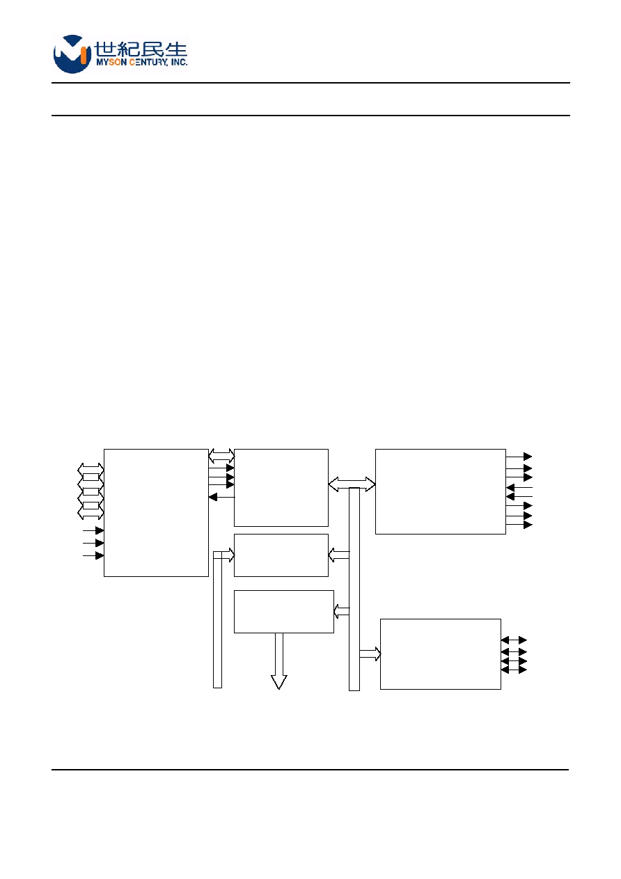
GENERAL DESCRIPTIONS
The MTV212M32 micro-controller is an 8051 CPU core embedded device specially tailored to Monitor
applications. It includes an 8051 CPU core, 512-byte SRAM, SYNC processor, 14 built-in PWM DACs, VESA
DDC interface, 3-channel A/D converter and a 32K-byte internal program Flash-ROM.
BLOCK DIAGRAM
P1.0-7
P2.0-2,P2.4-7
P3.4-5
X1
P0.0-7
RD
WR
ALE
INT1
X2
8051
P3.2-0
RST
P0.0-7
RD
WR
ALE
INT1
XFR
STOUT
HBLANK
VBLANK
HSYNC
VSYNC
HCLAMP
HALFV
HALFH
H/VSYNC
CONTROL
ISCL
ISDA
HSCL
HSDA
DDC & IIC
INTERFACE
ADC
AD0-2
14 CHANNEL
PWM DAC
MTV212M32
Page 3 of 26
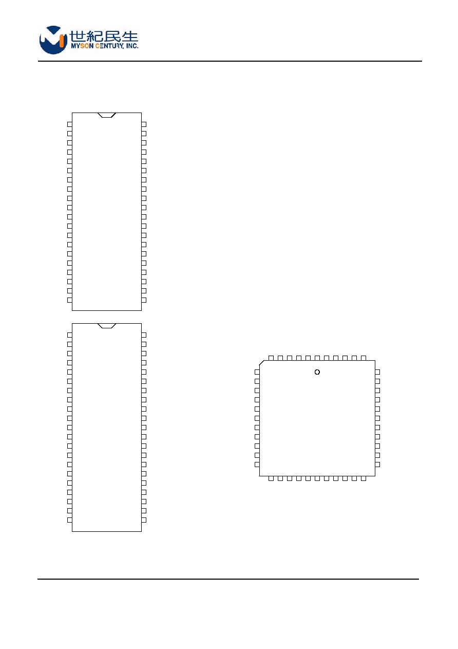
PIN CONNECTION
Note: As long as the pin sequence is not changed, the 42 pin SDIP's pin-out is negotiable according to
customer's demand.
MTV212M32
40 Pin
PDIP
DA2/P5.2
40
1
39
38
37
36
35
34
33
32
31
30
29
28
27
26
25
24
23
22
21
2
3
4
5
6
7
8
9
10
11
12
13
14
15
16
17
18
19
20
DA1/P5.1
DA0/P5.0
RST
VDD
VSS
X2
X1
ISDA/P3.4/T0
ISCL/P3.5/T1
STOUT/P4.2
P2.2/AD2
P1.0
P1.1
P3.2/INT0
P1.2
P1.3
P1.4
P1.5
P1.6
HSYNC
DA3/P5.3
VSYNC
DA4/P5.4
DA8/HALFH
DA9/HALFV
DA5/P5.5
HBLANK/P4.1
DA7/HCLAMP
DA6/P5.6
VBLANK/P4.0
P2.7/DA13
P2.5/DA11
P2.4/DA10
P2.6/DA12
HSCL/P3.0/Rxd
P2.0/AD0
P2.1/AD1
HSDA/P3.1/Txd
P1.7
MTV212M32
42 Pin
SDIP
DA2/P5.2
40
1
39
38
37
36
35
34
33
32
31
30
29
28
27
26
25
24
23
22
21
2
3
4
5
6
7
8
9
10
11
12
13
14
15
16
17
18
19
20
DA1/P5.1
DA0/P5.0
RST
VDD
VSS
X2
X1
ISDA/P3.4/T0
ISCL/P3.5/T1
STOUT/P4.2
P2.2/AD2
P1.0
P1.1
P3.2/INT0
P1.2
P1.3
NC
NC
NC
HSYNC
DA3/P5.3
VSYNC
DA4/P5.4
DA8/HALFH
DA9/HALFV
DA5/P5.5
HBLANK/P4.1
DA7/HCLAMP
DA6/P5.6
VBLANK/P4.0
P1.6
P2.4/DA10
P1.5
HSCL/P3.0/Rxd
P2.0/AD0
P2.1/AD1
HSDA/P3.1/Txd
P1.7
42
41
P2.5/DA11
P2.6/DA12
P1.4
MTV212M32
44 Pin
PLCC
7
8
9
10
11
12
13
14
15
16
17
39
38
37
36
35
34
33
32
31
30
29
P1.6
24
P1.7
P2.1/AD1
P1.5
P2.0/AD0
HSDA/P3.1/Txd
P1.1
P3.2/INT0
P1.2
P1.3
P1.4
23
22
21
20
28
27
26
25
NC
6
5
4
3
2
1
44
43
42
41
40
NC
NC
DA0/P5.0
DA1/P5.1
DA2/P5.2
VSYNC
HSYNC
DA3/P5.3
DA4/P5.4
DA5/P5.5
19
18
RST
VDD
VSS
X2
X1
ISDA/P3.4/T0
ISCL/P3.5/T1
STOUT/P4.2
P2.2/AD2
P1.0
P2.3/AD3
P2.4/DA10
HSCL/P3.0/Rxd
P2.5/DA11
P2.6/DA12
DA8/HALFH
DA9/HALFV
HBLANK/P4.1
DA7/HCLAMP
DA6/P5.6
VBLANK/P4.0
P2.7/DA13
MTV212M32
Page 4 of 26
PIN DESCRIPTION
Name Type
Description
DA2/P5.2
I/O
PWM DAC output (5V open drain) / General purpose I/O (5V open drain).
DA1/P5.1
I/O
PWM DAC output (5V open drain) / General purpose I/O (5V open drain).
DA0/P5.0
I/O
PWM DAC output (5V open drain) / General purpose I/O (5V open drain).
RST
I
Active high reset.
VDD
-
Positive Power Supply.
P2.3/AD3
I/O
General purpose I/O (CMOS output or 8051 standard) / ADC Input.
VSS
-
Ground.
X2
O
Oscillator output.
X1
I
Oscillator input.
ISDA/P3.4/T0
I/O
Master IIC data (5V open drain) / General purpose I/O (8051 standard) / T0
ISCL/P3.5/T1
I/O
Master IIC clock (5V open drain) / General purpose I/O (8051 standard) / T1
STOUT/P4.2
O
Self-test video output (CMOS) / General purpose Output (CMOS).
P2.2/AD2
I/O
General purpose I/O (CMOS output or 8051 standard) / ADC Input.
P1.0
I/O
General purpose I/O (CMOS output or 8051 standard).
P1.1
I/O
General purpose I/O (CMOS output or 8051 standard).
P3.2/INT0
I
General purpose Input / INT0.
P1.2
I/O
General purpose I/O (CMOS output or 8051 standard).
P1.3
I/O
General purpose I/O (CMOS output or 8051 standard).
P1.4
I/O
General purpose I/O (CMOS output or 8051 standard).
P1.5
I/O
General purpose I/O (CMOS output or 8051 standard).
P1.6
I/O
General purpose I/O (CMOS output or 8051 standard).
P1.7
I/O
General purpose I/O (CMOS output or 8051 standard).
P2.1/AD1
I/O
General purpose I/O (CMOS output or 8051 standard) / ADC Input.
P2.0/AD0
I/O
General purpose I/O (CMOS output or 8051 standard) / ADC Input.
HSDA/P3.1/Txd
I/O
Slave IIC data (5V open drain) / General purpose I/O (8051 standard) / Txd
HSCL/P3.0/Rxd
I/O
Slave IIC clock (5V open drain) / General purpose I/O (8051 standard) / Rxd
P2.4/DA10
I/O
General purpose I/O (CMOS output or 8051 standard) / PWM DAC output (CMOS).
P2.5/DA11
I/O
General purpose I/O (CMOS output or 8051 standard) / PWM DAC output (CMOS).
P2.6/DA12
I/O
General purpose I/O (CMOS output or 8051 standard) / PWM DAC output (CMOS).
P2.7/DA13
I/O
General purpose I/O (CMOS output or 8051 standard) / PWM DAC output (CMOS).
DA6/P5.6
I/O
PWM DAC output (CMOS) / General purpose I/O (CMOS output or open drain I/O).
DA7/HCLAMP
O
PWM DAC output (CMOS) / Hsync clamp pulse output (CMOS).
VBLANK/P4.0
O
Vertical blank (CMOS) / General purpose Output (CMOS).
HBLANK/P4.1
O
Horizontal blank (CMOS) / General purpose Output (CMOS).
DA9/HALFV
O
PWM DAC output (5V open drain) / vsync half freq. output (5V open drain).
DA8/HALFH
O
PWM DAC output (5V open drain) / hsync half freq. output (5V open drain).
DA5/P5.5
I/O
PWM DAC output (CMOS) / General purpose I/O (CMOS output or open drain I/O).
DA4/P5.4
I/O
PWM DAC output (CMOS) / General purpose I/O (CMOS output or open drain I/O).
DA3/P5.3
I/O
PWM DAC output (CMOS) / General purpose I/O (CMOS output or open drain I/O).
HSYNC
I
Horizontal SYNC or Composite SYNC Input.
VSYNC
I
Vertical SYNC input.