MTV412M
8051 Embedded Monitor Controller 128K Flash Type with ISP
sales@myson.com.tw
www.myson.com.tw
Rev. 1.3 November 2002
page 1 of 34
Myson Century, Inc.
Taiwan:
No. 2, Industry East Rd. III,
Science-Based Industrial Park, Hsin-Chu, Taiwan
Tel: 886-3-5784866 Fax: 886-3-5784349
USA:
4020 Moorpark Avenue Suite 115
San Jose, CA, 95117
Tel: 408-243-8388 Fax: 408-243-3188
FEATURES
· 8051 core, 12MHz operating frequency with double CPU clock option
· 0.35um process; 3.3V/5V power supply; 5V I/O tolerant
· 1024-byte RAM; 128K-byte program Flash-ROM support In System Programming (ISP) without boot code
· Maximum 14 channels of PWM DAC
· Maximum 38 (44-pin) or 36 (42-pin) I/O pins
· SYNC processor for composite separation/insertion, H/V polarity/frequency check and polarity adjustment
· Clock output to drive other devices
· Built-in low power reset circuit
· Compliant with VESA DDC1/2B/2Bi/2B+ standard
· Triple slave IIC addresses; two H/W auto transfer DDC1/DDC2x data for both D-sub and DVI interfaces
· Single master IIC interface for internal device communication
· Maximum 4-channel 8-bit A/D converter
· Flash-ROM program code protection selection
· 42-pin SDIP or 44-pin PLCC/PQFP package
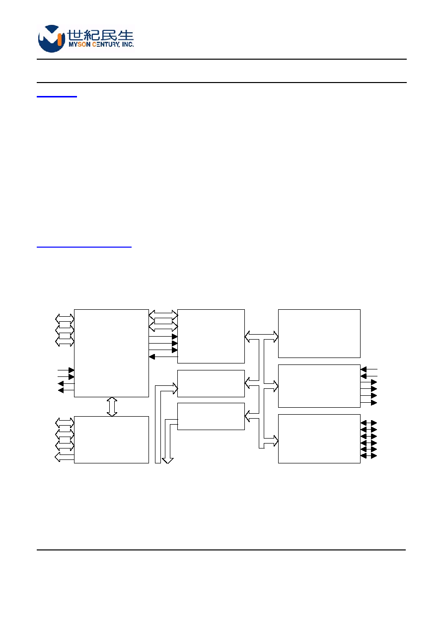
GENERAL DESCRIPTIONS
The MTV412M micro-controller is an 8051 CPU core embedded device targeted for LCD Monitor, LCD TV or
smart panel applications. It includes an 8051 CPU core, 1024-byte SRAM, 14 PWM DACs, VESA DDC for both
D-sub and DVI interfaces, 4-channel 8-bit ADC, hardware ISP without boot code and a 128K-byte internal
program Flash-ROM in 42-pin SDIP, 44-pin PLCC/PQFP package.
P0.0-7
P2.0-3
RD
WR
ALE
INT1
8051
CORE
P1.0-7
P3.0-2
P3.4
RST
X1
X2
ADC
AD0-3
PWM DAC
DA0-13
XFR
P0.0-7
P2.0-3
RD
WR
ALE
INT1
AUXRAM &
DDCRAM1 &
DDCRAM2
DDC & IIC
INTERFACE
ISCL
ISDA
HSCL1
HSDA1
HSCL2
HSDA2
P6.0-7
P5.0-6
AUX
I/O
P4.0-2
P7.0-7
HSYNC
VSYNC
HBLANK
VBLANK
H/VSYNC
CONTROL
HCLAMP
VCOAST
CKO
MTV412M
page 2 of 34
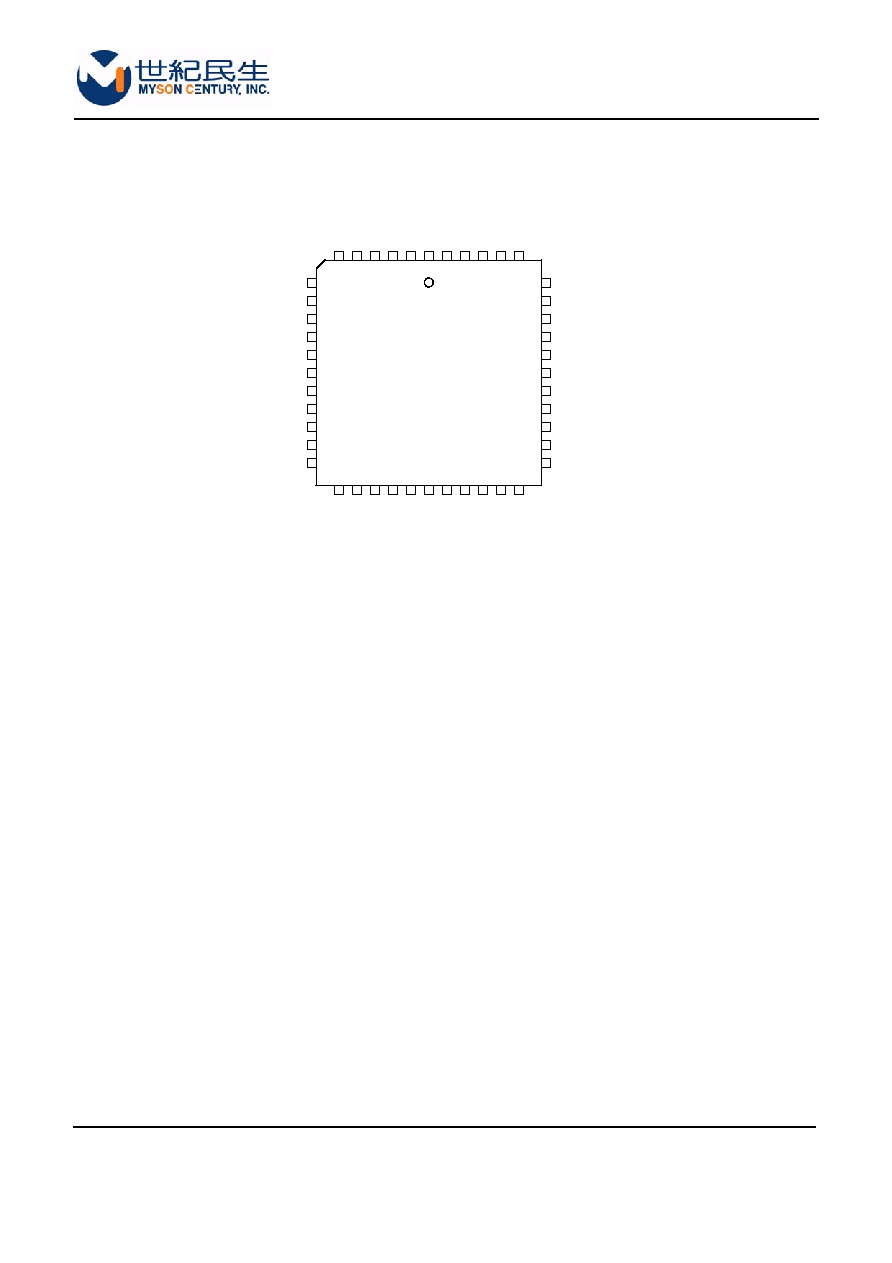
PIN CONNECTION
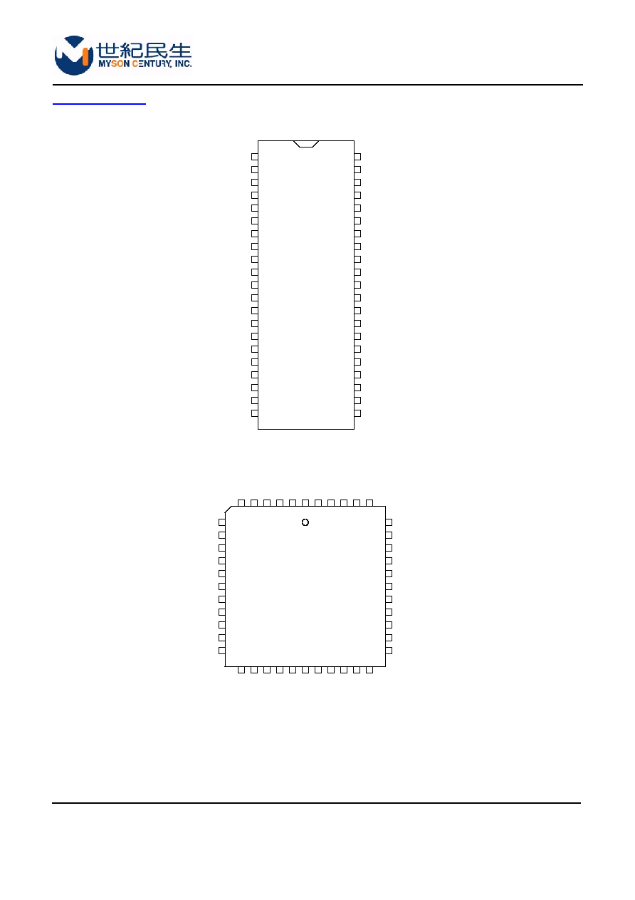
MTV412MV
44-pin
PLCC
7
8
9
10
11
12
13
14
15
16
17
39
38
37
36
35
34
33
32
31
30
29
P1.6
24
P1.7
P6.1/AD1
P1.5
P6.0/AD0
HSDA/P3.1/Txd
P1.1
P3.2/INT0
P1.2
P1.3
P1.4
23
22
21
20
28
27
26
25
HSCL2/P7.5
6
5
4
3
2
1
44
43
42
41
40
HSDA2/P7.6
VDD3
DA0/P5.0
DA1/P5.1
DA2/P5.2
VSYNC/P7.4
HSYNC/P7.3
DA3/P5.3
DA4/P5.4
DA5/P5.5
19
18
RST
VDD
VSS
X2
X1
ISDA/P3.4/T0
ISCL/P7.7
VCOAST/P4.2
P6.2/AD2
P1.0
P6.3/AD3
P6.4/DA10
HSCL/P3.0/Rxd
P6.5/DA11
P6.6/DA12
DA8/P7.1
DA9/P7.2
HBLANK/P4.1
DA7/P7.0/HCLAMP
DA6/P5.6/CKO
VBLANK/P4.0
P6.7/DA13
MTV412MS
42-pin
SDIP
DA2/P5.2
40
1
39
38
37
36
35
34
33
32
31
30
29
28
27
26
25
24
23
22
21
2
3
4
5
6
7
8
9
10
11
12
13
14
15
16
17
18
19
20
DA1/P5.1
DA0/P5.0
RST
VDD
VSS
VDD3
HSDA2/P7.6
HSCL2/P7.5
HSYNC/P7.3
DA3/P5.3
VSYNC/P7.4
DA4/P5.4
DA8/P7.1
DA9/P7.2
DA5/P5.5
HBLANK/P4.1
DA7/P7.0/HCLAMP
DA6/P5.6/CKO
VBLANK/P4.0
42
41
ISDA/P3.4/T0
ISCL/P7.7
P4.2
P6.2/AD2
P1.0
P1.1
P3.2/INT0
P1.2
P1.3
P1.4
X2
X1
P6.6/DA12
P6.5/DA11
HSCL1/P3.0/Rxd
HSDA1/P3.1/Txd
P6.4/DA10
P6.0/AD0
P1.7
P1.6
P6.1/AD1
P1.5
MTV412M
page 4 of 34
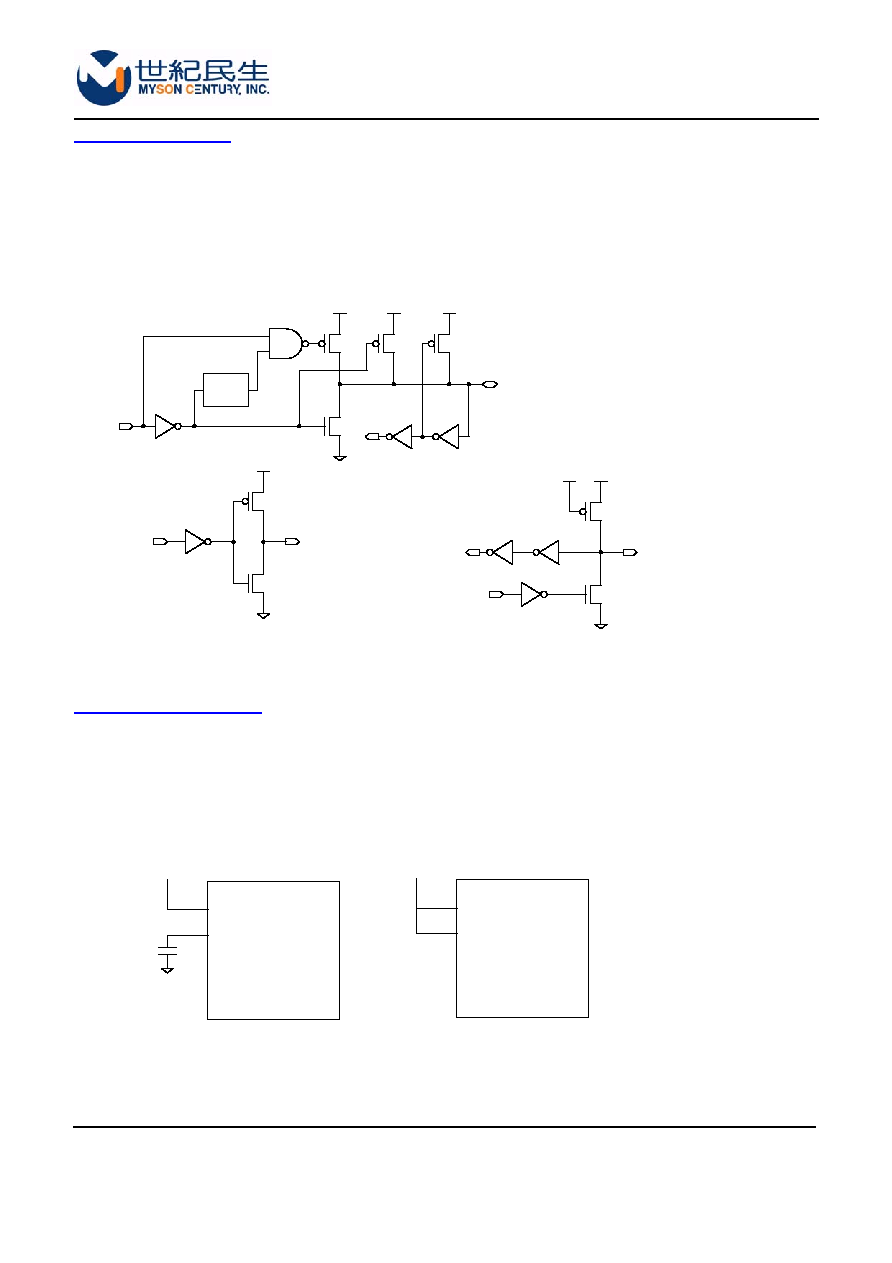
PIN CONFIGURATION
A "CMOS output pin" means it can sink and drive at least 4mA current. It is not recommended to use such pin
as input function.
A "open drain pin" means it can sink at least 4mA current but only drive 10~20uA to VDD. It can be used as
input or output function and needs an external pull up resistor.
A "8051 standard pin" is a pseudo open drain pin. It can sink at least 4mA current when output is at low level,
and drives at least 4mA current for 160nS when output transits from low to high, then keeps driving at 100uA to
maintain the pin at high level. It can be used as input or output function. It needs an external pull up resistor
when driving heavy load device.
POWER CONFIGURATION
The MTV412M can work on 5V or 3.3V power supply system. In 5V power system, the VDD pin is connected to
5V power and the VDD3 needs an external capacitor, all output pins can swing from 0~5V, input pins can
accept 0~5V input range. And ADC conversion range is 5V. However, X1 and X2 pins must be kept below 3.3V.
In 3.3V power system, the VDD and VDD3 are connected to 3.3V power, all output pins swing from 0~3.3V,
HSYNC, VSYNC and open drain pin can accept 0~5V input range, other pins must be kept below 3.3V. And the
ADC conversion range is 3.3V.
8051 Standard Pin
4mA
4mA
Output
Data
Pin
CMOS Output Pin
Open Drain Pin
2 OSC
period
delay
4mA
10uA
Output
Data
120uA
Pin
4mA
Input
Data
No Current
4mA
Output
Data
Pin
Input
Data
3.3V
VDD
VDD3
MTV412M in
3.3V System
VDD
VDD3
5V
10u
MTV412M in
5V System
MTV412M
page 5 of 34
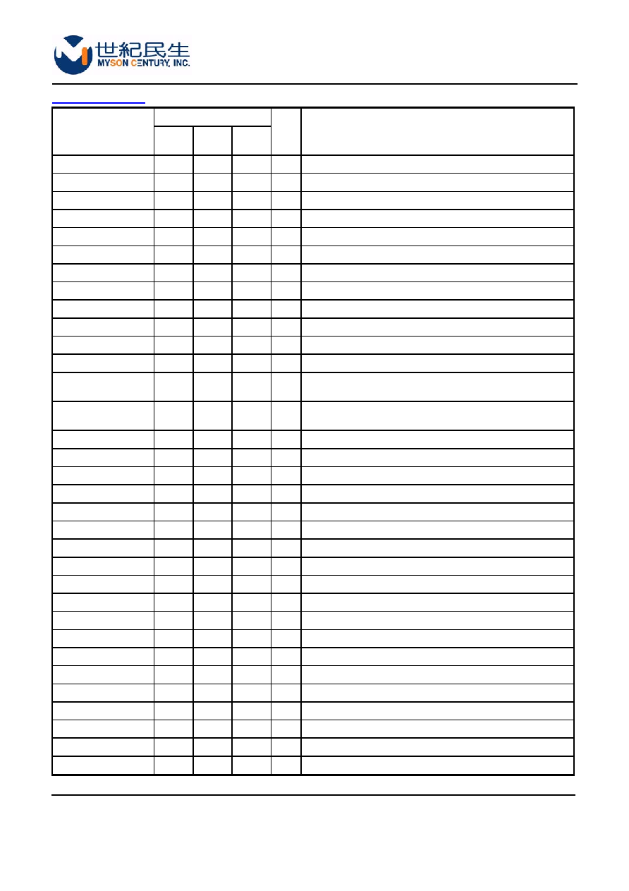
PIN DESCRIPTION
Package
Name
42-pin
SDIP
44-pin
PLCC
44-pin
PQFP
Type
Description
VDD3
4 4 42
O
3.3V core power
VDD
8 8 2 -
5V or 3.3V Positive Power Supply
VSS
9 10 4 -
Ground
X2
10 11 5 O
Oscillator output
X1
11 12 6 I
Oscillator input
RST
7 7 1 I
Active high reset
DA0/P5.0
3 3 41
I/O
PWM DAC output / General purpose I/O (CMOS)
DA1/P5.1
2 2 40
I/O
PWM DAC output / General purpose I/O (CMOS)
DA2/P5.2
1 1 39
I/O
PWM DAC output / General purpose I/O (CMOS)
DA3/P5.3
40 42 36
I/O
PWM DAC output / General purpose I/O (CMOS)
DA4/P5.4
39 41 35
I/O
PWM DAC output / General purpose I/O (CMOS)
DA5/P5.5
38 40 34
I/O
PWM DAC output / General purpose I/O (CMOS)
DA6/P5.6/CKO
32 34 28
I/O
PWM DAC output / General purpose I/O / Oscillator Freq.
clock output (CMOS)
DA7/P7.0/HCLAMP
33 35 29
I/O
PWM DAC output / General purpose I/O / Hsync clamp pulse
output (CMOS)
DA8/P7.1
37
39
33
I/O
PWM DAC output / General purpose I/O (open drain)*
DA9/P7.2
36
38
32
I/O
PWM DAC output / General purpose I/O (open drain)*
HSCL1/P3.0/Rxd
28 29 23
I/O
Slave IIC 1 clock / General purpose I/O / Rxd (open drain)
HSDA1/P3.1/Txd
27 28 22
I/O
Slave IIC 1 data / General purpose I/O / Txd (open drain)
HSCL2/P7.5
6 6 44
I/O
Slave IIC 2 clock / General purpose I/O (open drain)
HSDA2/P7.6
5 5 43
I/O
Slave IIC 2 data / General purpose I/O (open drain)
P3.2/INT0
18 19 13
I/O
General purpose I/O / INT0 (8051 standard)
ISDA/P3.4/T0
12
13
7
I/O
Master IIC data / General purpose I/O / T0 (open drain)*
ISCL/P7.7
13
14
14
I/O
Master IIC clock / General purpose I/O (open drain)*
P1.0
16 17 11
I/O
General purpose I/O (CMOS output or 8051 standard)
P1.1
17 18 12
I/O
General purpose I/O (CMOS output or 8051 standard)
P1.2
19 20 14
I/O
General purpose I/O (CMOS output or 8051 standard)
P1.3
20 21 15
I/O
General purpose I/O (CMOS output or 8051 standard)
P1.4
21 22 16
I/O
General purpose I/O (CMOS output or 8051 standard)
P1.5
22 23 17
I/O
General purpose I/O (CMOS output or 8051 standard)
P1.6
23 24 18
I/O
General purpose I/O (CMOS output or 8051 standard)
P1.7
24 25 19
I/O
General purpose I/O (CMOS output or 8051 standard)
P6.0/AD0
26 27 21
I/O
General purpose I/O / ADC Input (CMOS)
P6.1/AD1
25 26 20
I/O
General purpose I/O / ADC Input (CMOS)