173
TK-RELAYS
ULTRA LOW PROFILE 2 AMP.
POLARIZED RELAY
TESTING
mm
inch
9.0
.354
10.6
.417
4.0
.157
FEATURES
∑ Low profile 4 mm .157 inch height
∑ High contact capacity: 2 A
∑ Surge withstand voltage between contact and coil: 2,500 V
(Bellcore rating)
SPECIFICATIONS
Contact
Note:
f
1This value can change due to the switching frequency, environmental conditions,
and desired reliability level, therefore it is recommended to check this with the ac-
tual load.
Characteristics
Arrangement
1 Form C
Initial contact resistance, max.
(By voltage drop 6 V DC 1 A)
50 m
Contact material
Gold-clad silver alloy
Rating
Nominal switching capacity
(resistive load)
2 A 30 V DC
Max. Switching power
(resistive load)
60 W
Max. switching voltage
220 V DC
Max. switching current
2 A
Min. switching capacity
f
1
10
µ
A 10 mV DC
Nominal
operating
power
Single side stable
140 mW (1.5 to 12 V DC)
270 mW (24 V DC)
1 coil latching
100 mW (1.5 to 12 V DC)
150 mW (24 V DC)
2 coil latching
200 mW (1.5 to 9 V DC)
250 mW (12 V DC)
400 mW (24 V DC)
Expected
life (min.
operations)
Mechanical (at 180 cpm)
10
8
(Single side stable)
5
◊
10
7
(1 or 2 coil latching)
Electrical
(at 20 cpm)
2 A 30 V DC
resistive
10
5
Initial insulation resistance*
1
Min. 1,000 M
(at 500 V DC)
Initial
breakdown
voltage
Between open
contacts
750 Vrms for 1 min.
(Detection current: 10 mA)
Between contact and
coil
1,500 Vrms for 1 min.
(Detection current: 10 mA)
FCC surge voltage between open
contacts (10
◊
160
µ
s)
1,500 V
Surge voltage between contacts
and coil (2
◊
10
µ
s) [Bellcore]
2,500 V
Temperature rise*
2
(at 20
∞
C)
Max. 50
∞
C
Operate time [Set time]*
3
(at 20
∞
C)
Max. 3 ms (Approx. 1.5 ms)
[Max. 3 ms (Approx. 1 ms)]
Release time [Reset time]*
4
(at 20
∞
C)
Max. 2 ms (Approx. 1 ms)
[Max. 3 ms (Approx. 1 ms)]
Shock resistance
Functional*
5
Min. 750 m/s
2
{75 G}
Destructive*
6
Min. 1,000 m/s
2
{100 G}
Vibration
resistance
Functional*
7
196 m/s
2
{20G}, 10 to 55 Hz at
double amplitude of 3.3 mm
Destructive
294 m/s
2
{30G}, 10 to 55 Hz at
double amplitude of 5 mm
Conditions for
operation, trans-
port and storage*
8
(Not freezing and
condensing at low
temperature)
Ambient
temperature*
9
≠40
∞
C to +85
∞
C
≠40
∞
F to +185
∞
F
Humidity
5 to 85% R.H.
Unit weight
Approx. 1 g .
035 oz.
Remarks
* Specifications will vary with foreign standards certification ratings.
*
1
Measurement at same location as "Initial breakdown voltage" section.
*
2
By resistive method, nominal voltage applied to the coil; contact carrying current:
2 A.
*
3
Nominal voltage applied to the coil, excluding contact bounce time.
*
4
Nominal voltage applied to the coil, excluding contact bounce time without diode.
*
5
Half-wave pulse of sine wave: 6 ms; detection time: 10
µ
s.
*
6
Half-wave pulse of sine wave: 6 ms.
*
7
Detection time: 10
µ
s.
*
8
Refer to 4. Conditions for operation, transport and storage mentioned in Cautions
for use (Page 178).
*
9
The maximum ambient temperature allows for coil temperature rise at maximum
allowable coil voltage.
As for the applicable range of continuous carrying current against temperature,
please refer to "Maximum value of continuous carrying current" chart. (Page 175)
ORDERING INFORMATION
EX. TK
Contact arrangement
Terminal shape
1: 1 Form C
Nil: Standard PC board terminal
Nil: Single side stable
1.5, 3, 4.5, 5, 6,
9, 12, 24V
L: 1 coil latching
L2: 2 coil latching
H: Self-clinching terminal
Operating function
Coil voltage (DC)
L2
H
12V
1
TK
174
TYPES AND COIL DATA (at 20
∞
C
68
∞
F
)
1. Single side stable
2. 1 Coil latching
3. 2 Coil latching
Notes:
1. Specified value of the pick-up, drop-out, set and reset voltage is with the condition of square wave coil pulse.
2. Standard packing: Tube: 50 pcs.; Case; 1,000 pcs.
3. In case of 5 V transistor drive circuit, it is recommended to use 4.5 V type relay.
Part No.
Nominal
voltage,
V DC
Pick-up
voltage,
V DC (max.)
Drop-out
voltage,
V DC (min.)
Nominal
operating
current,
mA (
±
10%)
Coil
resistance,
(
±
10%)
Nominal
operating
power,
mW
Max.
allowable
voltage,
V DC
Standard PC
board terminal
Self-clinching
terminal
TK1-1.5 V
TK1-H-1.5 V
1.5
1.125
0.15
93.8
16
140
2.25
TK1-3 V
TK1-H-3 V
3
2.25
0.3
46.7
64.3
140
4.5
TK1-4.5 V
TK1-H-4.5 V
4.5
3.38
0.45
31.1
145
140
6.7
TK1-5 V
TK1-H-5 V
5
3.75
0.5
28.1
178
140
7.5
TK1-6 V
TK1-H-6 V
6
4.5
0.6
23.3
257
140
9
TK1-9 V
TK1-H-9 V
9
6.75
0.9
15.5
579
140
13.5
TK1-12 V
TK1-H-12 V
12
9
1.2
11.7
1,028
140
18
TK1-24 V
TK1-H-24 V
24
18
2.4
11.3
2,133
270
28.8
Part No.
Nominal
voltage,
V DC
Set voltage,
V DC (max.)
Reset voltage,
V DC (max.)
Nominal
operating
current,
mA (
±
10%)
Coil
resistance,
(
±
10%)
Nominal
operating
power,
mW
Max.
allowable
voltage,
V DC
Standard PC
board terminal
Self-clinching
terminal
TK1-L-1.5 V
TK1-L-H-1.5 V
1.5
1.125
1.125
66.7
22.5
100
2.25
TK1-L-3 V
TK1-L-H-3 V
3
2.25
2.25
33.3
90
100
4.5
TK1-L-4.5 V
TK1-L-H-4.5 V
4.5
3.38
3.38
22.2
202.5
100
6.7
TK1-L-5 V
TK1-L-H-5 V
5
3.75
3.75
20
250
100
7.5
TK1-L-6 V
TK1-L-H-6 V
6
4.5
4.5
16.7
360
100
9
TK1-L-9 V
TK1-L-H-9 V
9
6.75
6.75
11.1
810
100
13.5
TK1-L-12 V
TK1-L-H-12 V
12
9
9
8.3
1,440
100
18
TK1-L-24 V
TK1-L-H-24 V
24
18
18
6.3
3,840
150
28.8
Part No.
Nominal
voltage,
V DC
Set voltage,
V DC (max.)
Reset voltage,
V DC (max.)
Nominal
operating
current,
mA (
±
10%)
Coil
resistance,
(
±
10%)
Nominal
operating
power,
mW
Max.
allowable
voltage,
V DC
Standard PC
board terminal
Self-clinching
terminal
TK1-L2-1.5 V
TK1-L2-H-1.5 V
1.5
1.125
1.125
133.9
11.2
200
2.25
TK1-L2-3 V
TK1-L2-H-3 V
3
2.25
2.25
66.7
45
200
4.5
TK1-L2-4.5 V
TK1-L2-H-4.5 V
4.5
3.38
3.38
44.5
101.2
200
6.7
TK1-L2-5 V
TK1-L2-H-5 V
5
3.75
3.75
40
125
200
7.5
TK1-L2-6 V
TK1-L2-H-6 V
6
4.5
4.5
33.3
180
200
9
TK1-L2-9 V
TK1-L2-H-9 V
9
6.75
6.75
22.2
405
200
13.5
TK1-L2-12 V
TK1-L2-H-12 V
12
9
9
20.8
576
250
14.4
TK1-L2-24 V
TK1-L2-H-24 V
24
18
18
16.7
1,440
400
26.4
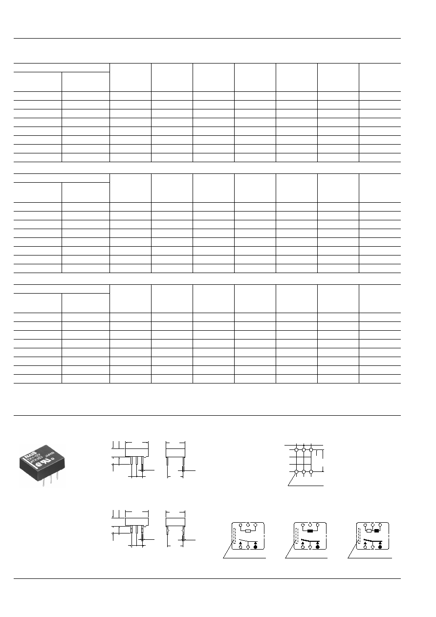
DIMENSIONS
mm
inch
Standard PC board terminal
Self-clinching terminal
General tolerance:
±
0.3
±
.012
10.6
3.75
9
3.5
0.25
2.54
7.62
0.5
0.25
4
.148
.354
.417
.138
.010
.100
2.54
.100
.300
.020
.010
.157
10.6
3.75
9
3.5
0.25
2.54
7.62
0.5
0.25
4
.148
.354
.417
.138
.010
.100
2.54
.100
.300
.020
.010
.157
PC board pattern (Copper-side view)
2.54
.100
2.54
.100
2.54
.100
6-1.0 dia. holes
6-.040 dia. holes
.300
+
+
+
+
+
+
7.62
Tolerance:
±
0.1
±
.004
Schematic (Bottom view)
∑ Single side stable
(Deenergized condition)
∑ 1-coil latching
(Reset condition)
∑ 2-coil latching
(Reset condition)
1
2
3
6
5
4
Direction indication*
-
+
Direction indication*
1
2
3
6
5
4
-
+
1
2
3
6
5
4
Direction indication*
+
-
+
*Orientation stripe located on top of relay.
TK
175
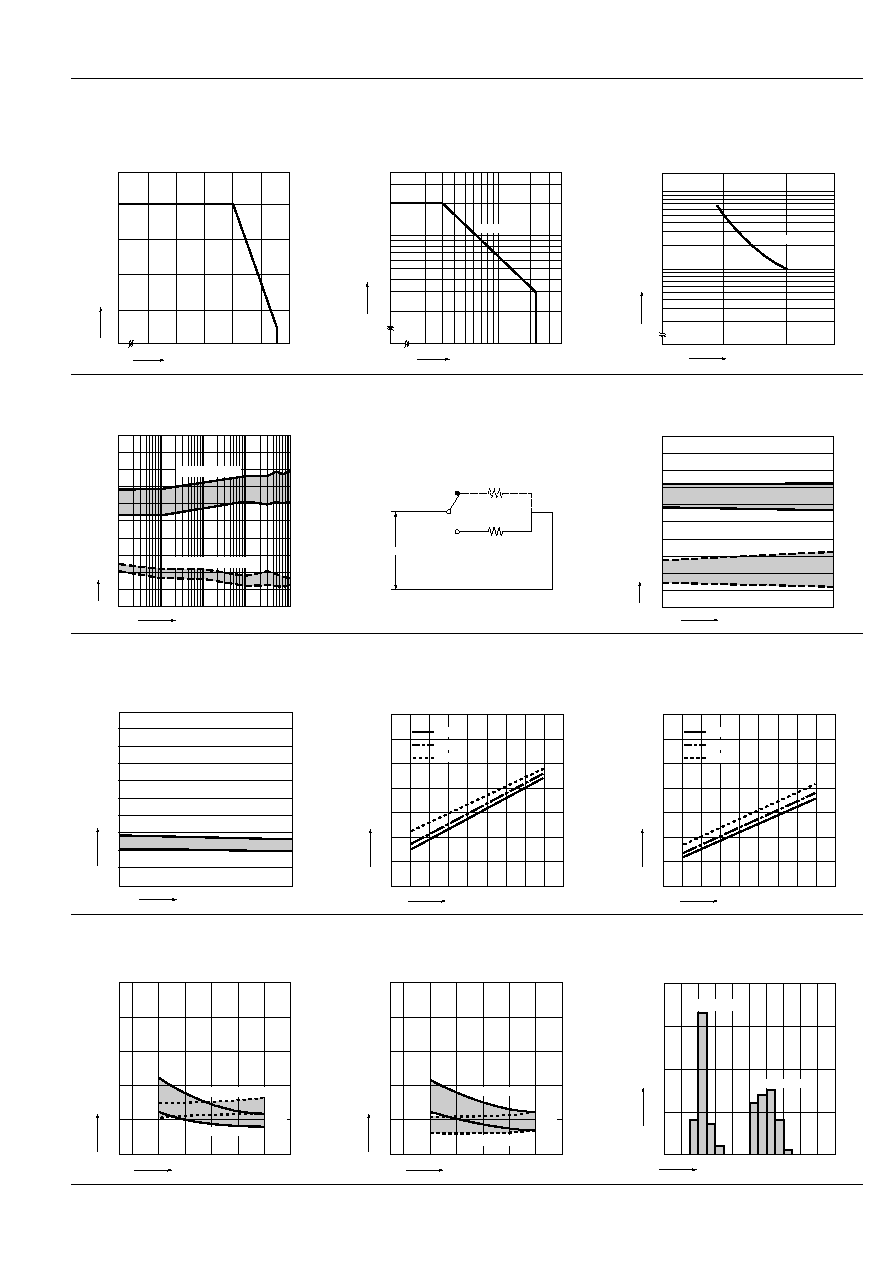
REFERENCE DATA
1. Maximum value of continuous carrying current
Test conditions:
Coil applied voltage: 110% of rated voltage
Continuous carrying current: 1,000 hours
2. Maximum switching capacity
3. Life curve
Continuous carrying current, A
Ambient temperature,
∞
C
2
1
0
70
80
60
50
40
90
85
Switching current, A
Switching voltage, V
200 300
100
30
50
20
DC load
0.2
0.3
0.4
0.5
1.0
2.0
3.0
No. of operations,
◊
10
4
Switching current, A
10
100
2
1
0
30 V DC resistive
4. Mechanical life
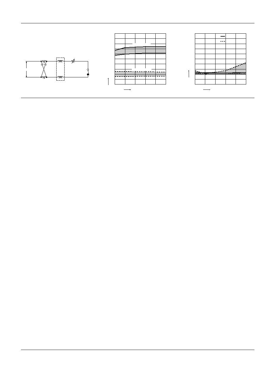
Tested sample: TK1-12V, 8 pcs.
Switching frequency: 30 Hz
5. Electrical life (DC load)
Tested sample: TK1-12V, 10 pcs.
Condition: 2 A 30 V DC resistive load, 20 cpm
Circuit
Change of pick-up and drop-out voltage
Ratio against the rated voltage, %V
No. of operations,
◊
10
4
0
10
20
30
40
50
60
70
80
90
100
10
100
1,000
10,000
Drop-out voltage
Pick-up voltage
Max.
Min.
Max.
Min.
30 V DC
+
≠
No. of operations,
◊
10
4
0
10
20
30
40
50
60
70
80
90
100
10
Pick-up voltage
Drop-out voltage
Max.
Min.
Max.
Min.
Ratio against the rated voltage, %V
Change of contact resistance
6. Coil temperature rise
Tested sample: TK1-12V, 6 pcs.
Measured portion: Inside the coil
Carrying current: 0 A, 1 A, 2 A
Ambient temperature: 25
∞
C
77
∞
F
Ambient temperature: 70
∞
C
158
∞
F
No . of operations,
◊
10
4
Max.
Min.
10
0
10
20
30
40
50
60
70
80
90
100
Contact resistance, m
x
-
0
10
20
30
40
50
60
80
90 100 110 120 130 140 150
Coil applied voltage, %V
Temperature rise,
∞
C
0 A
1 A
2 A
x
-
0
10
20
30
40
50
60
80
90 100 110 120 130 140 150
Coil applied voltage, %V
Temperature rise,
∞
C
0 A
1 A
2 A
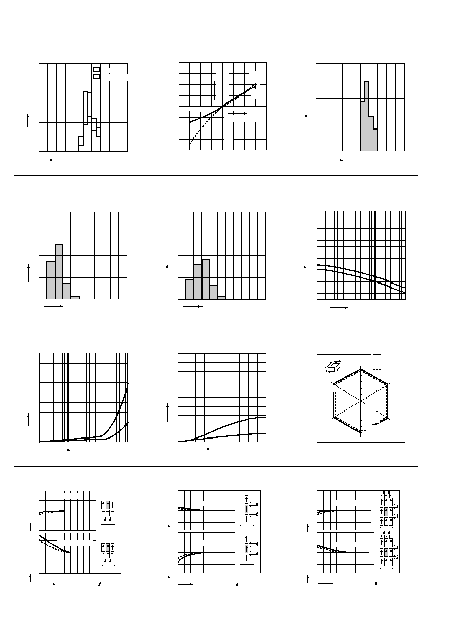
7. Operate/release time characteristics
Tested sample: TK1-5 V, 50 pcs.
<With diode>
<Without diode>
8. Distribution of pick-up and drop-out voltage
Tested sample: TK1-5V, 50 pcs.
Min.
Max.
Max.
Min.
Coil applied voltage, %V
80
90
100
110
120
0
1
2
3
4
Operate/release time, ms
Operate time
Release time
Operate time
Release time
Min.
Coil applied voltage, %V
80
90
100
110
120
0
1
2
3
4
Operate/release time, ms
Max.
Max.
Min.
Min.
Operate time
Release time
Ratio agaenst the rated voltage, %V
Quamtity
0
10
20
30
10 20 30 40 50 60 70 80 90 100
Drop-out voltage
Pick-up voltage
TK
176
9. Distribution of set and reset voltage
Tested sample: TK1-L2-12V, 50 pcs.
10. Ambient temperature characteristics
Tested sample: TK1-12V, 5 pcs.
11. Distribution of contact resistance
Tested sample TK1-5V, 50 pcs. (50
◊
2 contacts)
,,,
,,,,,
,,,,,,
,,,,,,
,,,,,
,,,,
,,
,
,,,
,,,,
,,,,,
,,,,,
,,,,,
,,,
,
Quantity
Ratio against the rated voltage, %V
,
,
,
,,
,,
,,
,,
,,
,,
,,
,,
,,
,,
,,
,,
,,
,,
,,
10
10
20
20 30 40 50 60 70 80 90 100
0
Set voltage
Reset voltage
Pick-up
voltage
Drop-out
voltage
Ambient
temperature,
∞
C
Variation ratio, %
0
10
20
≠20
0
≠10
≠20
≠30
≠40
≠40
40
60
80
20
30
40
x
-
x
-
Quantity
4
8
12 16 20 24 28 32 36 40
10
20
30
40
50
0
Contact resistance. m
12. Distribution of operate/release bounce time
Tested sample: TK1-5V, 50 pcs.
<Operate bounce time>
<Release bounce time>
13.-(1) High-frequency characteristics
Isolation characteristics
Quantity
Operate bounce time, ms
0.1 0.2 0.3 0.4 0.5 0.6 0.7 0.8 0.9 1.0
0
10
20
30
Quantity
Release bounce time, ms
0.1 0.2 0.3 0.4 0.5 0.6 0.7 0.8 0.9 1.0
0
10
20
30
10
100
100
1,000
50
0
Frequency,MHz
Isolation, dB
N.O.
N.C.
13.-(2) High-frequency characteristics
Insertion loss characteristics
13.-(3) High-frequency characteristics
V.S.W.R.
14. Malfunctional shock
Tested sample: TK1-12V, 6 pcs. (single side stable);
TK1-L2-12V, 6 pcs. (latching)
10
100
1,000
0
0.2
0.4
0.6
0.8
1.0
1.2
1.4
1.6
1.8
Frequency,MHz
Insertion loss, dB
N.O.
N.C.
Frequency,GHz
N.O.
N.C.
V.S.W.R.
1.0
1.2
1.4
1.6
1.8
2.0
2.2
2.4
2.6
2.8
3.0
0
0.5
1
Y
Y
,
Y
,
Y
Z
,
Z
,
Z
Z
X
,
X
,
X
X
980m/s
2
980m/s
2
980m/s
2
980m/s
2
980m/s
2
980m/s
2
784m/s
2
588m/s
2
392m/s
2
196m/s
2
Deenergized
condition
(Reset state)
Energized
condition
(Set state)
15.-(1) Influence of adjacent mounting
15.-(2) Influence of adjacent mounting
15.-(3) Influence of adjacent mounting
Inter-relay distance , mm
inch
0
5
.197
Rate of change, %
Rate of change, %
ON
ON
ON
OFF OFF
OFF
0
5
≠5
0
5
≠5
Pick-up voltage
Drop-out voltage
Inter-relay distance , mm
inch
0
5
.197
0
5
≠5
0
5
≠5
Rate of change, %
Rate of change, %
ON
ON
OFF
OFF
OFF
Drop-out voltage
Pick-up voltage
ON
Inter-relay distance , mm
inch
0
5
.197
Rate of change, %
Rate of change, %
OFF
ON
0
5
≠5
0
5
≠5
Pick-up voltage
Drop-out voltage
OFF
OFF
OFF
ON
ON
ON
TK
177
16. Actual load test (35 mA 48 V DC wire spring
relay load)
Circuit
Change of pick-up and drop-out voltage
Change of contact resistance
Wire spning relay
458
0.08
µ
F
0.08
µ
F
48 V DC
5
+
≠
4
458
100
90
80
70
60
50
40
30
20
10
0
10
Max.
Max.
Min.
Min.
20
30
40
50
Pick-up voltage
Drop-out voltage
No. of operations,
◊
10
4
Ratio against the rated voltage, %V
100
90
80
70
60
50
40
30
20
10
0
10
Max.
N.C.
N.O.
Max.
Min.
Min.
20
30
40
50
No. of operations,
◊
10
4
Contact resistance, m
For Cautions for Use, see Page 178 and 179.
9/1/2000
All Rights Reserved, © Copyright Matsushita Electric Works, Ltd.
Go To Online Catalog