
NanoAmp Solutions, Inc.
1982 Zanker Road, San Jose, CA 95112
ph: 408-573-8878, FAX: 408-573-8877
www.nanoamp.com
N04L0850C1A
Stock No. 23175-02 11/02
1
The specifications of this device are subject to change without notice. For latest documentation see http://www.nanoamp.com.
4Mb Ultra-Low Power Asynchronous CMOS SRAM
512Kx8 bit
Overview
The N04L0850C1A is an integrated memory
device containing a 4 Mbit Static Random Access
Memory organized as 524,288 words by 8 bits. The
device is designed and fabricated using
NanoAmp's advanced CMOS technology to
provide both high-speed performance and ultra-low
power. The device operates with a single chip
enable (CE), write enable (WE) and output enable
(OE) controls to allow for easy memory expansion.
The N04L0850C1A is optimal for various
applications where low-power is critical such as
battery backup and hand-held devices. The device
can operate over a very wide temperature range of
-40
o
C to +85
o
C and is available in a JEDEC
standard 32-pin SOP package.
Features
� Wide Power Supply Range
4.5 to 5.5 Volts
� Very low standby current
1.5�A at 5.0V (Typical)
� Very low operating current
20.0mA at 5.0V and 1�s (Typical)
� Simple memory control
Single Chip Enable (CE)
Output Enable (OE) for memory expansion
� Low voltage data retention
Vcc = 1.5V
� Very fast output enable access time
35ns OE access time
� Automatic power down to standby mode
� TTL compatible three-state output driver
Pin Configuration
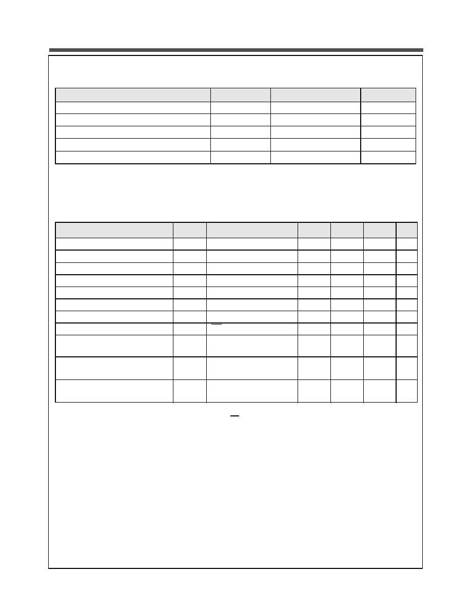
Product Family
Part Number
Package
Type
Operating
Temperature
Power
Supply (Vcc)
Speed
Standby
Current (I
SB
),
Typical
Operating
Current (Icc),
Typical
N04L0850C1AS-70I 32 - SOP I
-40
o
C to +85
o
C
4.5V - 5.5V
70ns
1.5
�
A
20 mA @
1MHz
N04L0850C1A
SOP
A18
A16
A14
A12
A7
A6
A5
A4
A3
A2
A1
A0
I/O0
I/O1
I/O2
Vss
Vcc
A15
A17
WE
A13
A8
A9
A11
OE
A10
CE
I/O7
I/O6
I/O5
I/O4
I/O3
1
2
3
4
5
6
7
8
9
10
11
12
13
14
15
16
32
31
30
29
28
27
26
25
24
23
22
21
20
19
18
17
Pin Descriptions
Pin Name
Pin Function
A
0
-A
18
Address Inputs
WE
Write Enable Input
CE
Chip Enable Input
OE
Output Enable Input
I/O
0
-I/O
7
Data Inputs/Outputs
V
CC
Power
V
SS
Ground

Stock No. 23175-02 11/02
2
The specifications of this device are subject to change without notice. For latest documentation see http://www.nanoamp.com.
NanoAmp Solutions, Inc.
N04L0850C1A
Functional Block Diagram
Functional Description
CE
WE
OE
I/O
0
- I/O
7
MODE
POWER
H
X
X
High Z
Standby
1
1. When the device is in standby mode, control inputs (WE and OE), address inputs and data input/outputs are internally
isolated from any external influence and disabled from exerting any influence externally.
Standby
L
L
X
2
2. When WE is invoked, the OE input is internally disabled and has no effect on the circuit.
Data In
Write
2
Active
L
H
L
Data Out
Read
Active
L
H
H
High Z
Active
Active
Capacitance
1
1. These parameters are verified in device characterization and are not 100% tested
Item
Symbol
Test Condition
Min
Max
Unit
Input Capacitance
C
IN
V
IN
= 0V, f = 1 MHz, T
A
= 25
o
C
6
pF
I/O Capacitance
C
I/O
V
IN
= 0V, f = 1 MHz, T
A
= 25
o
C
8
pF
Control
Logic
Decode
Logic
Address
Inputs
A
0
- A
18
Input/
Output
Mux
and
Buffers
I/O
0
- I/O
7
Address
512K x 8 bit
RAM Array
CE
WE
OE
Stock No. 23175-02 11/02
3
The specifications of this device are subject to change without notice. For latest documentation see http://www.nanoamp.com.
NanoAmp Solutions, Inc.
N04L0850C1A
Absolute Maximum Ratings
1
1. Stresses greater than those listed above may cause permanent damage to the device. This is a stress rating only and functional
operation of the device at these or any other conditions above those indicated in the operating section of this specification is not
implied. Exposure to absolute maximum rating conditions for extended periods may affect reliability.
Item
Symbol
Rating
Unit
Voltage on any pin relative to V
SS
V
IN,OUT
�0.5 to +6.0
V
Power Dissipation
P
D
1
W
Storage Temperature
T
STG
�60 to 150
o
C
Operating Temperature
T
A
-40 to +85
o
C
Soldering Temperature and Time
T
SOLDER
240
o
C, 10sec(Lead only)
o
C
Operating Characteristics (Over Specified Temperature Range)
Item
Symbol
Test Conditions
Min.
Typ
1
1. Typical values are measured at Vcc=Vcc Typ., T
A
=25�C and not 100% tested.
Max
Unit
Supply Voltage
V
CC
4.5
5.0
5.5
V
Data Retention Voltage
V
DR
Chip Disabled
2
1.5
V
Input High Voltage
V
IH
2.2
V
CC
+0.3
V
Input Low Voltage
V
IL
�0.5
0.8
V
Output High Voltage
V
OH
I
OH
= -1mA
2.4
V
Output Low Voltage
V
OL
I
OL
= 2mA
0.4
V
Input Leakage Current
I
LI
V
IN
= 0 to V
CC
1
�
A
Output Leakage Current
I
LO
OE = V
IH
or Chip Disabled
1
�
A
Read/Write Operating Supply Current
@ Min Cycle Time
I
CC2
V
CC
=5.0 V, V
IN
=V
IH
or V
IL
Chip Enabled, I
OUT
= 0
50.0
mA
Maximum Standby Current
2
2. This device assumes a standby mode if the chip is disabled (CE high). In order to achieve low standby current all inputs must be
within 0.2 volts of either VCC or VSS.
I
SB
VIN
Vcc-0.2V or
0.2V
Chip Disabled, V
CC
= 5.0V
1.5
25
�
A
Maximum Data Retention Current
2
I
DR
VIN
Vcc-0.2V or
0.2V
Chip Disabled, V
CC
= 1.5V
0.2
2.5
�
A

Stock No. 23175-02 11/02
4
The specifications of this device are subject to change without notice. For latest documentation see http://www.nanoamp.com.
NanoAmp Solutions, Inc.
N04L0850C1A
Timing Test Conditions
Item
Input Pulse Level
0.1V
CC
to 0.9 V
CC
Input Rise and Fall Time
5ns
Input and Output Timing Reference Levels
0.5 V
CC
Output Load
CL = 100pF
Operating Temperature
-40 to +85
o
C
Timing
Item
Symbol
Min
Max
Units
Read
Cycle
Read Cycle Time
t
RC
70
ns
Address Access Time
t
AA
70
ns
Chip Enable to Valid Output
t
CO
70
ns
Output Enable to Valid Output
t
OE
35
ns
Chip Enable to Low-Z output
t
LZ
10
ns
Output Enable to Low-Z Output
t
OLZ
10
ns
Chip Disable to High-Z Output
t
HZ
0
35
ns
Output Disable to High-Z Output
t
OHZ
0
30
ns
Output Hold from Address Change
t
OH
10
ns
Write
Cycle
Write Cycle Time
t
WC
70
ns
Chip Enable to End of Write
t
CW
70
ns
Address Valid to End of Write
t
AW
70
ns
Write Pulse Width
t
WP
35
ns
Address Setup Time
t
AS
0
ns
Write Recovery Time
t
WR
0
ns
Write to High-Z Output
t
WHZ
30
ns
Data to Write Time Overlap
t
DW
30
ns
Data Hold from Write Time
t
DH
0
ns
End Write to Low-Z Output
t
OW
5
ns

Stock No. 23175-02 11/02
5
The specifications of this device are subject to change without notice. For latest documentation see http://www.nanoamp.com.
NanoAmp Solutions, Inc.
N04L0850C1A
Timing of Read Cycle (CE = OE = V
IL
, WE = V
IH
)
Timing Waveform of Read Cycle (WE=V
IH
)
Address
Data Out
t
RC
t
AA
t
OH
Data Valid
Previous Data Valid
Address
OE
Data Valid
t
RC
t
AA
t
CO
t
HZ
t
OHZ
t
OLZ
t
OE
t
LZ
High-Z
Data Out
CE