
NT5DS64M4AT NT5DS64M4AW
NT5DS32M8AT NT5DS32M8AW
256Mb Double Data Rate SDRAM
REV 1.3
08/2002
1
©
NANYA TECHNOLOGY CORP
. All rights reserved.
NANYA TECHNOLOGY CORP. reserves the right to change Products and Specifications without notice.
Features
∑
Double data rate architecture: two data transfers per
clock cycle
∑
Bidirectional data strobe (DQS) is transmitted and
received with data, to be used in capturing data at the
receiver
∑
DQS is edge-aligned with data for reads and is center-
aligned with data for writes
∑
Differential clock inputs (CK and CK)
∑
Four internal banks for concurrent operation
∑
Data mask (DM) for write data
∑
DLL aligns DQ and DQS transitions with CK transitions
∑
Commands entered on each positive CK edge; data and
data mask referenced to both edges of DQS
∑
Burst lengths: 2, 4, or 8
∑
CAS Latency: 2, 2.5
∑
Auto Precharge option for each burst access
∑
Auto Refresh and Self Refresh Modes
∑
7.8
µ
s Maximum Average Periodic Refresh Interval
∑
2.5V (SSTL_2 compatible) I/O
∑
V
DDQ
= 2.5V
±
0.2V
∑
V
DD
= 2.5V
±
0.2V
∑
-7K parts support PC2100 modules.
-75B parts support PC2100 modules
-8B parts support PC1600 modules
Description
The 256Mb DDR SDRAM is a high-speed CMOS, dynamic
random-access memory containing 268,435,456 bits. It is
internally configured as a quad-bank DRAM.
The 256Mb DDR SDRAM uses a double-data-rate architec-
ture to achieve high-speed operation. The double data rate
architecture is essentially a 2n prefetch architecture with an
interface designed to transfer two data words per clock cycle
at the I/O pins. A single read or write access for the 256Mb
DDR SDRAM effectively consists of a single 2n-bit wide, one
clock cycle data transfer at the internal DRAM core and two
corresponding n-bit wide, one-half-clock-cycle data transfers
at the I/O pins.
A bidirectional data strobe (DQS) is transmitted externally,
along with data, for use in data capture at the receiver. DQS
is a strobe transmitted by the DDR SDRAM during Reads
and by the memory controller during Writes. DQS is edge-
aligned with data for Reads and center-aligned with data for
Writes.
The 256Mb DDR SDRAM operates from a differential clock
(CK and CK; the crossing of CK going high and CK going
LOW is referred to as the positive edge of CK). Commands
(address and control signals) are registered at every positive
edge of CK. Input data is registered on both edges of DQS,
and output data is referenced to both edges of DQS, as well
as to both edges of CK.
Read and write accesses to the DDR SDRAM are burst ori-
ented; accesses start at a selected location and continue for
a programmed number of locations in a programmed
sequence. Accesses begin with the registration of an Active
command, which is then followed by a Read or Write com-
mand. The address bits registered coincident with the Active
command are used to select the bank and row to be
accessed. The address bits registered coincident with the
Read or Write command are used to select the bank and the
starting column location for the burst access.
The DDR SDRAM provides for programmable Read or Write
burst lengths of 2, 4 or 8 locations. An Auto Precharge func-
tion may be enabled to provide a self-timed row precharge
that is initiated at the end of the burst access.
As with standard SDRAMs, the pipelined, multibank architec-
ture of DDR SDRAMs allows for concurrent operation,
thereby providing high effective bandwidth by hiding row pre-
charge and activation time.
An auto refresh mode is provided along with a power-saving
Power Down mode. All inputs are compatible with the JEDEC
Standard for SSTL_2. All outputs are SSTL_2, Class II com-
patible.
The functionality described and the timing specifications
included in this data sheet are for the DLL Enabled mode
of operation.
CAS Latency and Frequency
CAS Latency
Maximum Operating Frequency (MHz)*
DDR266A
(-7K)
DDR266B
(-75B)
DDR200
(-8B)
2
133
100
100
2.5
143
133
125
* Values are nominal (exact tCK should be used).

NT5DS64M4AT NT5DS64M4AW
NT5DS32M8AT NT5DS32M8AW
256Mb Double Data Rate SDRAM
REV 1.3
08/2002
2
©
NANYA TECHNOLOGY CORP
. All rights reserved.
NANYA TECHNOLOGY CORP. reserves the right to change Products and Specifications without notice.
Pin Configuration - 256Mb DDR SDRAM (x4 / x8)
1
2
3
4
5
6
9
10
11
12
13
14
7
8
15
16
17
18
19
20
21
22
66
65
64
63
62
61
58
57
56
55
54
53
60
59
52
51
50
49
48
47
46
45
23
24
25
44
43
42
26
27
41
40
28
29
30
31
32
33
39
38
37
36
35
34
V
DD
DQ0
V
DDQ
NC
DQ1
V
SSQ
V
DDQ
NC
DQ3
V
SSQ
NC
NC
NC
DQ2
V
DDQ
NC
NC
V
DD
NU
NC
WE
CAS
RAS
CS
NC
BA0
BA1
V
SS
DQ7
V
SSQ
NC
DQ6
V
DDQ
V
SSQ
NC
DQ4
V
DDQ
NC
NC
NC
DQ5
V
SSQ
DQS
NC
V
REF
V
SS
DM*
CK
CK
CKE
NC
A12
A11
A9
V
DD
NC
V
DDQ
NC
DQ0
V
SSQ
V
DDQ
NC
DQ1
V
SSQ
NC
NC
NC
NC
V
DDQ
NC
NC
V
DD
NU
NC
WE
CAS
RAS
CS
NC
BA0
BA1
V
SS
NC
V
SSQ
NC
DQ3
V
DDQ
V
SSQ
NC
DQ2
V
DDQ
NC
NC
NC
NC
V
SSQ
DQS
NC
V
REF
V
SS
DM*
CK
CK
CKE
NC
A12
A11
A9
A10/AP
A0
A1
A2
A3
V
DD
A10/AP
A0
A1
A2
A3
V
DD
A8
A7
A6
A5
A4
V
SS
A8
A7
A6
A5
A4
V
SS
Column Address Table
Organization
Column Address
64Mb x 4
A0-A9, A11
32Mb x 8
A0-A9
*DM is internally loaded to match DQ and DQS identically
.
NT5DS64M4AT
NT5DS32M8AT
64Mb x 4
32Mb x 8
66-pin Plastic TSOP-II 400mil

NT5DS64M4AT NT5DS64M4AW
NT5DS32M8AT NT5DS32M8AW
256Mb Double Data Rate SDRAM
REV 1.3
08/2002
3
©
NANYA TECHNOLOGY CORP
. All rights reserved.
NANYA TECHNOLOGY CORP. reserves the right to change Products and Specifications without notice.
Pin Configuration - 60 balls 0.8mmx1.0mm Pitch CSP Package
<Top View >
See the balls through the package.
A
B
C
D
E
F
G
H
J
K
L
M
A
B
C
D
E
F
G
H
J
K
L
M
64 X 4
32 X 8
1
VSSQ
NC
NC
NC
NC
VREF
NC
VDDQ
VSSQ
VDDQ
VSSQ
VSS
CLK
A12
A11
A8
A6
A4
2
VSS
DQ3
NC
DQ2
DQS
DQM
CLK
CKE
A9
A7
A5
VSS
3
VDD
DQ0
NC
DQ1
QFC
NC
WE
RAS
BA1
A0
A2
VDD
7
NC
VSSQ
VDDQ
VSSQ
VDDQ
VDD
CAS
CS
BA0
A10/AP
A1
A3
8
VDDQ
NC
NC
NC
NC
NC
9
VSSQ
NC
NC
NC
NC
VREF
1
DQ7
VDDQ
VSSQ
VDDQ
VSSQ
VSS
CLK
A12
A11
A8
A6
A4
2
VSS
DQ6
DQ5
DQ4
DQS
DQM
CLK
CKE
A9
A7
A5
VSS
3
VDD
DQ1
DQ2
DQ3
QFC
NC
WE
RAS
BA1
A0
A2
VDD
7
DQ0
VSSQ
VDDQ
VSSQ
VDDQ
VDD
CAS
CS
BA0
A10/AP
A1
A3
8
VDDQ
NC
NC
NC
NC
NC
9

NT5DS64M4AT NT5DS64M4AW
NT5DS32M8AT NT5DS32M8AW
256Mb Double Data Rate SDRAM
REV 1.3
08/2002
4
©
NANYA TECHNOLOGY CORP
. All rights reserved.
NANYA TECHNOLOGY CORP. reserves the right to change Products and Specifications without notice.
Input/Output Functional Description
Symbol
Type
Function
CK, CK
Input
Clock: CK and CK are differential clock inputs. All address and control input signals are sampled
on the crossing of the positive edge of CK and negative edge of CK. Output (read) data is refer-
enced to the crossings of CK and CK (both directions of crossing).
CKE, CKE0, CKE1
Input
Clock Enable: CKE HIGH activates, and CKE Low deactivates, internal clock signals and device
input buffers and output drivers. Taking CKE Low provides Precharge Power Down and Self
Refresh operation (all banks idle), or Active Power Down (row Active in any bank). CKE is syn-
chronous for power down entry and exit, and for self refresh entry. CKE is asynchronous for self
refresh exit. CKE must be maintained high throughout read and write accesses. Input buffers,
excluding CK, CK and CKE are disabled during Power Down. Input buffers, excluding CKE, are
disabled during self refresh. The standard pinout includes one CKE pin. Optional pinouts might
include CKE1 on a different pin, in addition to CKE0, to facilitate independent Power Down control
of stacked devices.
CS, CS0, CS1
Input
Chip Select: All commands are masked when CS is registered high. CS provides for external
bank selection on systems with multiple banks. CS is considered part of the command code. The
standard pinout includes one CS pin. Optional pinouts might include CS1 on a different pin, in
addition to CS0, to allow upper or lower deck selection on stacked devices.
RAS, CAS , WE
Input
Command Inputs: RAS, CAS and WE (along with CS) define the command being entered.
DM
Input
Input Data Mask: DM is an input mask signal for write data. Input data is masked when DM is
sampled high coincident with that input data during a Write access. DM is sampled on both edges
of DQS. Although DM pins are input only, the DM loading matches the DQ and DQS loading. Dur-
ing a Read, DM can be driven high, low, or floated.
BA0, BA1
Input
Bank Address Inputs: BA0 and BA1 define to which bank an Active, Read, Write or Precharge
command is being applied. BA0 and BA1 also determines if the mode register or extended mode
register is to be accessed during a MRS or EMRS cycle.
A0 - A12
Input
Address Inputs: Provide the row address for Active commands, and the column address and
Auto Precharge bit for Read/Write commands, to select one location out of the memory array in
the respective bank. A10 is sampled during a Precharge command to determine whether the Pre-
charge applies to one bank (A10 low) or all banks (A10 high). If only one bank is to be precharged,
the bank is selected by BA0, BA1. The address inputs also provide the op-code during a Mode
Register Set command.
DQ
Input/Output
Data Input/Output: Data bus.
DQS
Input/Output
Data Strobe: Output with read data, input with write data. Edge-aligned with read data, centered
in write data. Used to capture write data.
NC
No Connect: No internal electrical connection is present.
NU
Electrical connection is present. Should not be connected at second level of assembly.
V
DDQ
Supply
DQ Power Supply: 2.5V
±
0.2V.
V
SSQ
Supply
DQ Ground
V
DD
Supply
Power Supply: 2.5V
±
0.2V.
V
SS
Supply
Ground
V
REF
Supply
SSTL_2 reference voltage: (V
DDQ
/ 2)
±
1%.

NT5DS64M4AT NT5DS64M4AW
NT5DS32M8AT NT5DS32M8AW
256Mb Double Data Rate SDRAM
REV 1.3
08/2002
5
©
NANYA TECHNOLOGY CORP
. All rights reserved.
NANYA TECHNOLOGY CORP. reserves the right to change Products and Specifications without notice.
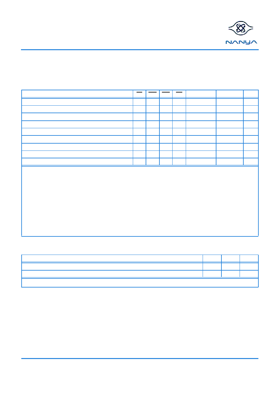
Ordering Information
Part Number
Org.
CAS
Latency
Clock
(MHz)
CAS
Latency
Clock
(MHz)
Speed
Package
NT5DS64M4AT-7K
x 4
2.5
143
2
133
DDR266A
66 pin TSOP-II
NT5DS32M8AT-7K
x 8
NT5DS64M4AT-75B
x 4
133
100
DDR266B
NT5DS32M8AT-75B
x 8
NT5DS64M4AT-8B
x 4
125
100
DDR200
NT5DS32M8AT-8B
x 8
NT5DS64M4AW-7K
x 4
2.5
143
2
133
DDR266A
60 ball CSP
NT5DS32M8AW-7K
x 8
NT5DS64M4AW-75B
x 4
133
100
DDR266B
NT5DS32M8AW-75B
x 8
NT5DS64M4AW-8B
x 4
125
100
DDR200
NT5DS32M8AW-8B
x 8
Note: At the present time, there are no plans to support DDR SDRAMs with the QFC function. All reference to QFC are for information.

NT5DS64M4AT NT5DS64M4AW
NT5DS32M8AT NT5DS32M8AW
256Mb Double Data Rate SDRAM
REV 1.3
08/2002
6
©
NANYA TECHNOLOGY CORP
. All rights reserved.
NANYA TECHNOLOGY CORP. reserves the right to change Products and Specifications without notice.
Block Diagram (64Mb x 4)
R
e
c
e
i
v
e
r
s
1
DQS
CK, CK
DLL
RAS
CAS
CK
CS
WE
CK
C
o
n
t
r
o
l
L
o
g
i
c
Column-Address
Counter/Latch
Mode
11
C
o
m
m
a
n
d
D
e
c
o
d
e
A0-A12,
BA0, BA1
CKE
13
15
I/O Gating
DM Mask Logic
Bank0
Memory
Array
(8192 x 1024 x 8)
Sense Amplifiers
Bank1
Bank2
Bank3
13
10
1
2
2
R
e
f
r
e
s
h
C
o
u
n
t
e
r
4
4
4
Input
Register
1
1
1
1
1
8
8
2
8
clk
out
Data
Mask
Data
CK,
COL0
COL0
COL0
clk
in
M
U
X
DQS
Generator
4
4
4
4
4
8
DQ0-DQ3,
DM
DQS
1
R
e
a
d
L
a
t
c
h
Write
FIFO
&
Drivers
Note: This Functional Block Diagram is intended to facilitate user understanding of the operation of
the device; it does not represent an actual circuit implementation.
Note: DM is a unidirectional signal (input only), but is internally loaded to match the load of the bidi-
rectional DQ and DQS signals.
Column
Decoder
1024
(x8)
R
o
w
-
A
d
d
r
e
s
s
M
U
X
Registers
1
3
8
1
9
2
B
a
n
k
0
R
o
w
-
A
d
d
r
e
s
s
L
a
t
c
h
&
D
e
c
o
d
e
r
8192
A
d
d
r
e
s
s
R
e
g
i
s
t
e
r
D
r
i
v
e
r
s
B
a
n
k
C
o
n
t
r
o
l
L
o
g
i
c
15
CK

NT5DS64M4AT NT5DS64M4AW
NT5DS32M8AT NT5DS32M8AW
256Mb Double Data Rate SDRAM
REV 1.3
08/2002
7
©
NANYA TECHNOLOGY CORP
. All rights reserved.
NANYA TECHNOLOGY CORP. reserves the right to change Products and Specifications without notice.
Block Diagram (32Mb x 8)
R
e
c
e
i
v
e
r
s
1
DQS
CK, CK
DLL
RAS
CAS
CK
CS
WE
CK
C
o
n
t
r
o
l
L
o
g
i
c
Column-Address
Counter/Latch
Mode
10
C
o
m
m
a
n
d
D
e
c
o
d
e
A0-A12,
BA0, BA1
CKE
15
15
I/O Gating
DM Mask Logic
Bank0
Memory
Array
(8192 x 512 x 16)
Sense Amplifiers
Bank1
Bank2
Bank3
13
9
1
2
2
R
e
f
r
e
s
h
C
o
u
n
t
e
r
8
8
8
Input
Register
1
1
1
1
1
16
16
2
16
clk
out
Data
Mask
Data
CK,
COL0
COL0
COL0
clk
in
M
U
X
DQS
Generator
8
8
8
8
8
16
DQ0-DQ7,
DM
DQS
1
R
e
a
d
L
a
t
c
h
Write
FIFO
&
Drivers
Note: This Functional Block Diagram is intended to facilitate user understanding of the operation of
the device; it does not represent an actual circuit implementation.
Note: DM is a unidirectional signal (input only), but is internally loaded to match the load of the bidi-
rectional DQ and DQS signals.
Column
Decoder
512
(x16)
R
o
w
-
A
d
d
r
e
s
s
M
U
X
Registers
1
3
8
1
9
2
B
a
n
k
0
R
o
w
-
A
d
d
r
e
s
s
L
a
t
c
h
&
D
e
c
o
d
e
r
8192
A
d
d
r
e
s
s
R
e
g
i
s
t
e
r
D
r
i
v
e
r
s
B
a
n
k
C
o
n
t
r
o
l
L
o
g
i
c
13
CK

NT5DS64M4AT NT5DS64M4AW
NT5DS32M8AT NT5DS32M8AW
256Mb Double Data Rate SDRAM
REV 1.3
08/2002
8
©
NANYA TECHNOLOGY CORP
. All rights reserved.
NANYA TECHNOLOGY CORP. reserves the right to change Products and Specifications without notice.
Functional Description
The 256Mb DDR SDRAM is a high-speed CMOS, dynamic random-access memory containing 268, 435, 456 bits. The 256Mb
DDR SDRAM is internally configured as a quad-bank DRAM.
The 256Mb DDR SDRAM uses a double-data-rate architecture to achieve high-speed operation. The double-data-rate architec-
ture is essentially a 2n prefetch architecture, with an interface designed to transfer two data words per clock cycle at the I/O
pins. A single read or write access for the 256Mb DDR SDRAM consists of a single 2n-bit wide, one clock cycle data transfer at
the internal DRAM core and two corresponding n-bit wide, one-half clock cycle data transfers at the I/O pins.
Read and write accesses to the DDR SDRAM are burst oriented; accesses start at a selected location and continue for a pro-
grammed number of locations in a programmed sequence. Accesses begin with the registration of an Active command, which is
then followed by a Read or Write command. The address bits registered coincident with the Active command are used to select
the bank and row to be accessed (BA0, BA1 select the bank; A0-A12 select the row). The address bits registered coincident
with the Read or Write command are used to select the starting column location for the burst access.
Prior to normal operation, the DDR SDRAM must be initialized. The following sections provide detailed infor-mation covering
device initialization, register definition, command descriptions and device operation.
Initialization
Only one of the following two conditions must be met.
∑ No power sequencing is specified during power up or power down given the following criteria:
V
DD
and V
DDQ
are driven from a single power converter output
V
TT
meets the specification
A minimum resistance of 42 ohms limits the input current from the VTT supply into any pin and
V
REF
tracks V
DDQ
/2
or
∑ The following relationships must be followed:
V
DDQ
is driven after or with V
DD
such that V
DDQ
< V
DD
+ 0.3V
V
TT
is driven after or with V
DDQ
such that V
TT
< V
DDQ
+ 0.3V
V
REF
is driven after or with V
DDQ
such that V
REF
< V
DDQ
+ 0.3V
The DQ and DQS outputs are in the High-Z state, where they remain until driven in normal operation (by a read access). After-
all power supply and reference voltages are stable, and the clock is stable, the DDR SDRAM requires a 200
µ
s delay prior to
applying an executable command.
Once the 200
µ
s delay has been satisfied, a Deselect or NOP command should be applied, and CKE must be brought HIGH.
Following the NOP command, a Precharge ALL command must be applied. Next a Mode Register Set command must be
issued for the Extended Mode Register, to enable the DLL, then a Mode Register Set command must be issued for the Mode
Register, to reset the DLL, and to program the operating parameters. 200 clock cycles are required between the DLL reset and
any read command. A Precharge ALL command should be applied, placing the device in the "all banks idle" state
Once in the idle state, two auto refresh cycles must be performed. Additionally, a Mode Register Set command for the Mode
Register, with the reset DLL bit deactivated (i.e. to program operating parameters without resetting the DLL) must be performed.
Following these cycles, the DDR SDRAM is ready for normal operation.
DDR SDRAM's may be reinitialized at any time during normal operation by asserting a valid MRS command to either the base
or extended mode registers without affecting the contents of the memory array. The contents of either the mode register or
extended mode register can be modified at any valid time during device operation without affecting the state of the internal
address refresh counters used for device refresh.

NT5DS64M4AT NT5DS64M4AW
NT5DS32M8AT NT5DS32M8AW
256Mb Double Data Rate SDRAM
REV 1.3
08/2002
9
©
NANYA TECHNOLOGY CORP
. All rights reserved.
NANYA TECHNOLOGY CORP. reserves the right to change Products and Specifications without notice.
Register Definition
Mode Register
The Mode Register is used to define the specific mode of operation of the DDR SDRAM. This definition includes the selection of
a burst length, a burst type, a CAS latency, and an operating mode. The Mode Register is programmed via the Mode Register
Set command (with BA0 = 0 and BA1 = 0) and retains the stored information until it is programmed again or the device loses
power (except for bit A8, which is self-clearing).
Mode Register bits A0-A2 specify the burst length, A3 specifies the type of burst (sequential or interleaved), A4-A6 specify the
CAS latency, and A7-A12 specify the operating mode.
The Mode Register must be loaded when all banks are idle, and the controller must wait the specified time before initiating the
subsequent operation. Violating either of these requirements results in unspecified operation.
Burst Length
Read and write accesses to the DDR SDRAM are burst oriented, with the burst length being programmable. The burst length
determines the maximum number of column locations that can be accessed for a given Read or Write command. Burst lengths
of 2, 4, or 8 locations are available for both the sequential and the interleaved burst types.
Reserved states should not be used, as unknown operation or incompatibility with future versions may result.
When a Read or Write command is issued, a block of columns equal to the burst length is effectively selected. All accesses for
that burst take place within this block, meaning that the burst wraps within the block if a boundary is reached. The block is
uniquely selected by A1-Ai when the burst length is set to two, by A
2
-Ai when the burst length is set to four and by A
3
-Ai when
the burst length is set to eight (where Ai is the most significant column address bit for a given configuration). The remaining
(least significant) address bit(s) is (are) used to select the starting location within the block. The programmed burst length
applies to both Read and Write bursts.

NT5DS64M4AT NT5DS64M4AW
NT5DS32M8AT NT5DS32M8AW
256Mb Double Data Rate SDRAM
REV 1.3
08/2002
10
©
NANYA TECHNOLOGY CORP
. All rights reserved.
NANYA TECHNOLOGY CORP. reserves the right to change Products and Specifications without notice.
Mode Register Operation
A8
A7
A6
A5
A4
CAS Latency
A3
A2
A1
A0
Burst Length
BT
Address Bus
CAS Latency
A6
A5
A4
Latency
0
0
0
Reserved
0
0
1
Reserved
0
1
0
2
0
1
1
Reserved
1
0
0
Reserved
1
0
1
Reserved
1
1
0
2.5
1
1
1
Reserved
Burst Length
A2
A1
A0
Burst Length
0
0
0
Reserved
0
0
1
2
0
1
0
4
0
1
1
8
1
0
0
Reserved
1
0
1
Reserved
1
1
0
Reserved
1
1
1
Reserved
BA1
BA0
A11 A10
A 9
0*
0*
Mode Register
Operating Mode
* BA0 and BA1 must be 0, 0 to select the Mode Register
(vs. the Extended Mode Register).
A12
- A9
A8
A 7
A6 - A0
Operating Mode
0
0
0
Valid
Normal operation
Do not reset DLL
0
1
0
Valid
Normal operation
in DLL Reset
0
0
1
VS**
Vendor-Specific
Test Mode
-
-
-
Reserved
A 3
Burst
Type
0
Sequential
1
Interleave
VS ** Vendor Specific
A12

NT5DS64M4AT NT5DS64M4AW
NT5DS32M8AT NT5DS32M8AW
256Mb Double Data Rate SDRAM
REV 1.3
08/2002
11
©
NANYA TECHNOLOGY CORP
. All rights reserved.
NANYA TECHNOLOGY CORP. reserves the right to change Products and Specifications without notice.
Notes:
1. For a burst length of two, A1-A i selects the two-data-element block; A0 selects the first access within the block.
2. For a burst length of four, A2-A i selects the four-data-element block; A0-A1 selects the first access within the block.
3. For a burst length of eight, A3-A i selects the eight-data- element block; A0-A2 selects the first access within the block.
4. Whenever a boundary of the block is reached within a given sequence above, the following access wraps within the block.
Burst Type
Accesses within a given burst may be programmed to be either sequential or interleaved; this is referred to as the burst type
and is selected via bit A3. The ordering of accesses within a burst is determined by the burst length, the burst type and the start-
ing column address, as shown in Burst Definition on page 11.
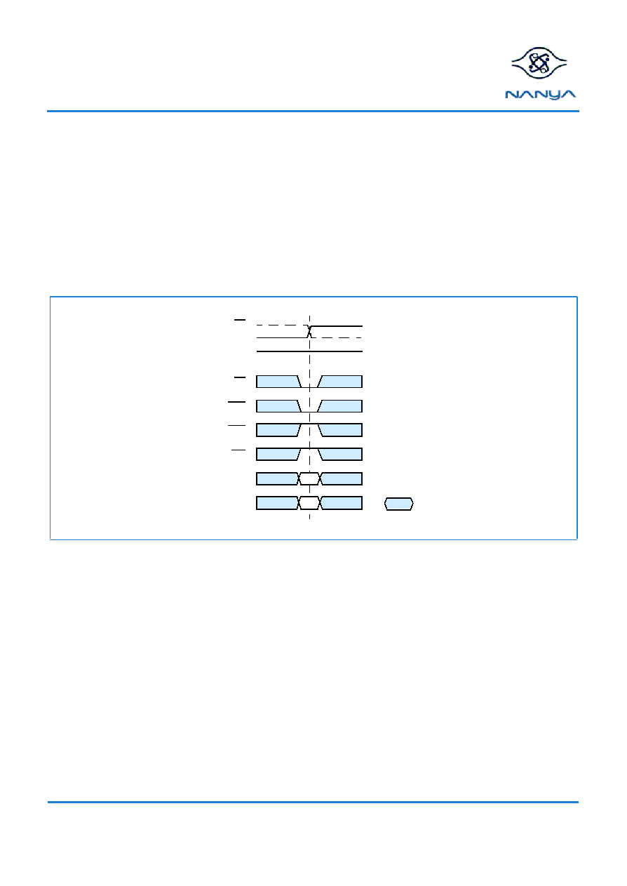
Read Latency
The Read latency, or CAS latency, is the delay, in clock cycles, between the registration of a Read command and the availability
of the first burst of output data. The latency can be programmed 2 or 2.5 clocks.
If a Read command is registered at clock edge n, and the latency is m clocks, the data is available nominally coincident with
clock edge n + m.
Reserved states should not be used as unknown operation or incompatibility with future versions may result.
Burst Definition
Burst Length
Starting Column Address
Order of Accesses Within a Burst
A2
A1
A0
Type = Sequential
Type = Interleaved
2
0
0-1
0-1
1
1-0
1-0
4
0
0
0-1-2-3
0-1-2-3
0
1
1-2-3-0
1-0-3-2
1
0
2-3-0-1
2-3-0-1
1
1
3-0-1-2
3-2-1-0
8
0
0
0
0-1-2-3-4-5-6-7
0-1-2-3-4-5-6-7
0
0
1
1-2-3-4-5-6-7-0
1-0-3-2-5-4-7-6
0
1
0
2-3-4-5-6-7-0-1
2-3-0-1-6-7-4-5
0
1
1
3-4-5-6-7-0-1-2
3-2-1-0-7-6-5-4
1
0
0
4-5-6-7-0-1-2-3
4-5-6-7-0-1-2-3
1
0
1
5-6-7-0-1-2-3-4
5-4-7-6-1-0-3-2
1
1
0
6-7-0-1-2-3-4-5
6-7-4-5-2-3-0-1
1
1
1
7-0-1-2-3-4-5-6
7-6-5-4-3-2-1-0
NT5DS64M4AT NT5DS64M4AW
NT5DS32M8AT NT5DS32M8AW
256Mb Double Data Rate SDRAM
REV 1.3
08/2002
12
©
NANYA TECHNOLOGY CORP
. All rights reserved.
NANYA TECHNOLOGY CORP. reserves the right to change Products and Specifications without notice.
Operating Mode
The normal operating mode is selected by issuing a Mode Register Set Command with bits A7-A12 to zero, and bits A0-A6 set
to the desired values. A DLL reset is initiated by issuing a Mode Register Set command with bits A7 and A9-A12 each set to
zero, bit A8 set to one, and bits A0-A6 set to the desired values. A Mode Register Set command issued to reset the DLL should
always be followed by a Mode Register Set command to select normal operating mode.
All other combinations of values for A7-A12 are reserved for future use and/or test modes. Test modes and reserved states
should not be used as unknown operation or incompatibility with future versions may result.
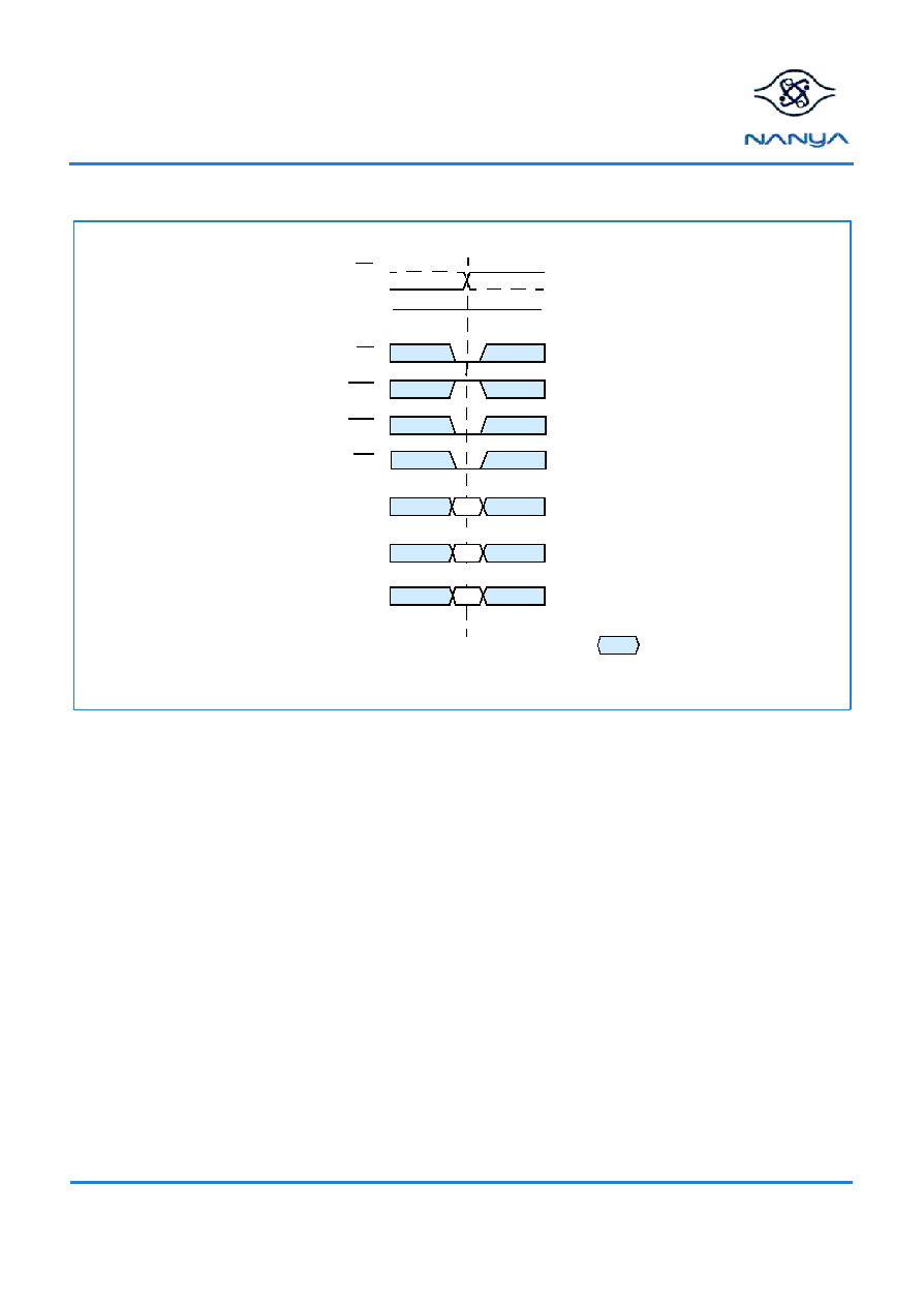
CAS Latencies
NOP
NOP
NOP
NOP
NOP
Read
CAS Latency = 2, BL = 4
Shown with nominal t
AC
, t
DQSCK
, and t
DQSQ
.
CK
CK
Command
DQS
DQ
Don't Care
CL=2
NOP
NOP
NOP
NOP
NOP
Read
CAS Latency = 2.5, BL = 4
CK
CK
Command
DQS
DQ
CL=2.5

NT5DS64M4AT NT5DS64M4AW
NT5DS32M8AT NT5DS32M8AW
256Mb Double Data Rate SDRAM
REV 1.3
08/2002
13
©
NANYA TECHNOLOGY CORP
. All rights reserved.
NANYA TECHNOLOGY CORP. reserves the right to change Products and Specifications without notice.
Extended Mode Register
The Extended Mode Register controls functions beyond those controlled by the Mode Register; these additional functions
include DLL enable/disable, bit A0; output drive strength selection, bit A1; and QFC output enable/disable, bit A2 (NTC
optional). These functions are controlled via the bit settings shown in the Extended Mode Register Definition. The Extended
Mode Register is programmed via the Mode Register Set command (with BA0 = 1 and BA1 = 0) and retains the stored informa-
tion until it is programmed again or the device loses power. The Extended Mode Register must be loaded when all banks are
idle, and the controller must wait the specified time before initiating any subsequent operation. Violating either of these require-
ments result in unspecified operation.
DLL Enable/Disable
The DLL must be enabled for normal operation. DLL enable is required during power up initialization, and upon returning to nor-
mal operation after having disabled the DLL for the purpose of debug or evaluation. The DLL is automatically disabled when
entering self refresh operation and is automatically re-enabled upon exit of self refresh operation. Any time the DLL is enabled,
200 clock cycles must occur to allow time for the internal clock to lock to the externally applied clock before a Read command
can be issued. This is the reason for introducing timing parameter t
XSRD
for DDR SDRAM's (Exit Self Refresh to Read Com-
mand). Non- Read commands can be issued 2 clocks after the DLL is enabled via the EMRS command (t
MRD
) or 10 clocks after
the DLL is enabled via self refresh exit command (t
XSNR
, Exit Self Refresh to Non-Read Command).
Output Drive Strength
The normal drive strength for all outputs is specified to be SSTL_2, Class II.
QFC Enable/Disable
The QFC signal is an optional DRAM output control used to isolate module loads (DIMMs) from the system memory bus by
means of external FET switches when the given module (DIMM) is not being accessed. The QFC function is an optional feature
for NTC and is not included on all DDR SDRAM devices. Refer to the DDR SDRAM Device Labeling Table for proper differenti-
ation when ordering DDR devices with or without the QFC function. The QFC output is an open drain driver and must be con-
nected to V
DDQ
through a pull up resistor at the board level if the QFC function is enabled. The recommended pull up resistance
is 150 ohms.

NT5DS64M4AT NT5DS64M4AW
NT5DS32M8AT NT5DS32M8AW
256Mb Double Data Rate SDRAM
REV 1.3
08/2002
14
©
NANYA TECHNOLOGY CORP
. All rights reserved.
NANYA TECHNOLOGY CORP. reserves the right to change Products and Specifications without notice.
Extended Mode Register Definition
A
8
A
7
A
6
A
5
A
4
A
3
A
2
A
1
A
0
Address Bus
Drive Strength
A
1
Drive Strength
0
Normal
1
Reserved
BA1
BA0
Operating Mode
A
11
A
10
A
9
0*
1*
* BA0 and BA1 must be 1, 0 to select the Extended Mode Register
Mode Register
Extended
DS
DLL
A
0
DLL
0
Enable
1
Disable
A12 - A3
A2 - A0
Operating Mode
0
Valid
Normal Operation
-
-
All other states
Reserved
(vs. the base Mode Register)
QFC
A
2
QFC
0
Disable
A
12
NT5DS64M4AT NT5DS64M4AW
NT5DS32M8AT NT5DS32M8AW
256Mb Double Data Rate SDRAM
REV 1.3
08/2002
15
©
NANYA TECHNOLOGY CORP
. All rights reserved.
NANYA TECHNOLOGY CORP. reserves the right to change Products and Specifications without notice.
Commands
Truth Tables 1a and 1b provide a reference of the commands supported by DDR SDRAM devices. A verbal description of each
commands follows.
Truth Table 1a: Commands
Name (Function)
CS
RAS
CAS
WE
Address
MNE
Notes
Deselect (Nop)
H
X
X
X
X
NOP
1, 9
No Operation (Nop)
L
H
H
H
X
NOP
1, 9
Active (Select Bank And Activate Row)
L
L
H
H
Bank/Row
ACT
1, 3
Read (Select Bank And Column, And Start Read Burst)
L
H
L
H
Bank/Col
Read
1, 4
Write (Select Bank And Column, And Start Write Burst)
L
H
L
L
Bank/Col
Write
1, 4
Burst Terminate
L
H
H
L
X
BST
1, 8
Precharge (Deactivate Row In Bank Or Banks)
L
L
H
L
Code
PRE
1, 5
Auto Refresh Or Self Refresh (Enter Self Refresh Mode)
L
L
L
H
X
AR / SR
1, 6, 7
Mode Register Set
L
L
L
L
Op-Code
MRS
1, 2
1. CKE is high for all commands shown except Self Refresh.
2. BA0, BA1 select either the Base or the Extended Mode Register (BA0 = 0, BA1 = 0 selects Mode Register; BA0 = 1, BA1 = 0 selects
Extended Mode Register; other combinations of BA0-BA1 are reserved; A0-A12 provide the op-code to be written to the selected Mode
Register.)
3. B A0-BA1 provide bank address and A0-A 12 provide row address.
4. BA0, BA1 provide bank address; A0-Ai provide column address (where i = 9 for x8 and 9, 11 for x4); A10 high enables the Auto Pre-
charge feature (nonpersistent), A10 low disables the Auto Precharge feature.
5. A10 LOW: BA0, BA1 determine which bank is precharged.
A10 HIGH: all banks are precharged and BA0, BA1 are "Don't Care."
6. This command is auto refreshif CKE is high; Self Refresh if CKE is low.
7. Internal refresh counter controls row and bank addressing; all inputs and I/Os are "Don't Care" except for CKE.
8. Applies only to read bursts with Auto Precharge disabled; this command is undefined (and should not be used) for read bursts with Auto
Precharge enabled or for write bursts
9. Deselect and NOP are functionally interchangeable.
Truth Table 1b: DM Operation
Name (Function)
DM
DQs
Notes
Write Enable
L
Valid
1
Write Inhibit
H
X
1
1. Used to mask write data; provided coincident with the corresponding data.

NT5DS64M4AT NT5DS64M4AW
NT5DS32M8AT NT5DS32M8AW
256Mb Double Data Rate SDRAM
REV 1.3
08/2002
16
©
NANYA TECHNOLOGY CORP
. All rights reserved.
NANYA TECHNOLOGY CORP. reserves the right to change Products and Specifications without notice.
Deselect
The Deselect function prevents new commands from being executed by the DDR SDRAM. The DDR SDRAM is
effectively deselected. Operations already in progress are not affected.
No Operation (NOP)
The No Operation (NOP) command is used to perform a NOP to a DDR SDRAM. This prevents unwanted commands from
being registered during idle or wait states. Operations already in progress are not affected.
Mode Register Set
The mode registers are loaded via inputs A0-A12, BA0 and BA1 while issuing the Mode Register Set Command. See mode reg-
ister descriptions in the Register Definition section. The Mode Register Set command can only be issued when all banks are idle
and no bursts are in progress. A subsequent executable command cannot be issued until t
MRD
is met.
Active
The Active command is used to open (or activate) a row in a particular bank for a subsequent access. The value on the BA0,
BA1 inputs selects the bank, and the address provided on inputs A0-A12 selects the row. This row remains active (or open) for
accesses until a Precharge (or Read or Write with Auto Precharge) is issued to that bank. A Precharge (or Read or Write with
Auto Precharge) command must be issued and completed before opening a different row in the same bank.
Read
The Read command is used to initiate a burst read access to an active (open) row. The value on the BA0, BA1 inputs selects
the bank, and the address provided on inputs A0-Ai, Aj (where [i = 9, j = don't care] for x8; where [i = 9, j = 11] for x4) selects the
starting column location. The value on input A10 determines whether or not Auto Precharge is used. If Auto Precharge is
selected, the row being accessed is precharged at the end of the Read burst; if Auto Precharge is not selected, the row remains
open for subsequent accesses.
Write
The Write command is used to initiate a burst write access to an active (open) row. The value on the BA0, BA1 inputs selects
the bank, and the address provided on inputs A0-Ai, Aj (where [i = 9, j = don't care] for x8; where [i = 9, j = 11] for x4) selects the
starting column location. The value on input A10 determines whether or not Auto Precharge is used. If Auto Precharge is
selected, the row being accessed is precharged at the end of the Write burst; if Auto Precharge is not selected, the row remains
open for subsequent accesses. Input data appearing on the DQs is written to the memory array subject to the DM input logic
level appearing coincident with the data. If a given DM signal is registered low, the corresponding data is written to memory; if
the DM signal is registered high, the corresponding data inputs are ignored, and a Write is not executed to that byte/column
location.
Precharge
The Precharge command is used to deactivate (close) the open row in a particular bank or the open row(s) in all banks. The
bank(s) will be available for a subsequent row access a specified time (t
RP
) after the Precharge command is issued. Input A10
determines whether one or all banks are to be precharged, and in the case where only one bank is to be precharged, inputs
BA0, BA1 select the bank. Otherwise BA0, BA1 are treated as "Don't Care." Once a bank has been precharged, it is in the idle
state and must be activated prior to any Read or Write commands being issued to that bank. A precharge command is treated
as a NOP if there is no open row in that bank, or if the previously open row is already in the process of precharging.
NT5DS64M4AT NT5DS64M4AW
NT5DS32M8AT NT5DS32M8AW
256Mb Double Data Rate SDRAM
REV 1.3
08/2002
17
©
NANYA TECHNOLOGY CORP
. All rights reserved.
NANYA TECHNOLOGY CORP. reserves the right to change Products and Specifications without notice.
Auto Precharge
Auto Precharge is a feature which performs the same individual-bank precharge function described above, but without requiring
an explicit command. This is accomplished by using A10 to enable Auto Precharge in conjunction with a specific Read or Write
command. A precharge of the bank/row that is addressed with the Read or Write command is automatically performed upon
completion of the Read or Write burst. Auto Precharge is nonpersistent in that it is either enabled or disabled for each individual
Read or Write command. Auto Precharge ensures that the precharge is initiated at the earliest valid stage within a burst. This is
determined as if an explicit Precharge command was issued at the earliest possible time without violating t
RAS
(min). The user
must not issue another command to the same bank until the precharge (t
RP
) is completed.
The NTC DDR SDRAM devices supports the optional t
RAS
lockout feature. This feature allows a Read command with Auto Pre-
charge to be issued to a bank that has been activated (opened) but has not yet satisfied the t
RAS
(min) specification. The t
RAS
lockout feature essentially delays the onset of the auto precharge operation until two conditions occur. One, the entire burst
length of data has been successfully prefetched from the memory array; and two, t
RAS
(min) has been satisfied.
As a means to specify whether a DDR SDRAM device supports the t
RAS
lockout feature, a new parameter has been defined,
t
RAP
(RAS Command to Read Command with Auto Precharge or better stated Bank Activate to Read Command with Auto Pre-
charge). For devices that support the t
RAS
lockout feature, t
RAP
= t
RCD
(min). This allows any Read Command (with or without
Auto Precharge) to be issued to an open bank once t
RCD
(min) is satisfied.
Burst Terminate
The Burst Terminate command is used to truncate read bursts (with Auto Precharge disabled). The most re-cently registered
Read command prior to the Burst Terminate command is truncated, as shown in the Operation section of this data sheet. Write
burst cycles are not to be terminated with the Burst Terminate command.
t
RAP
Definition
CK
CK
Command
DQ (BL=2)
t
RAPmin
NOP
ACT
NOP
RD A
NOP
NOP
NOP
NOP
ACT
NOP
NOP
t
RCDmin
t
RASmin
DQ0
DQ1
The above timing diagrams show the effects of t
RAP
for devices that support t
RAS
lockout. In these cases, the Read
with Auto Precharge command (RDA) is issued with t
RCD
(min) and dataout is available with the shortest latency from the
Bank Activate command (ACT). The internal precharge operation, however, does not begin until after t
RAS
(min) is satisfied.
CL=2, t
CK
=10ns
Command
DQ (BL=4)
NOP
ACT
NOP
RD A
NOP
NOP
NOP
NOP
ACT
NOP
NOP
DQ0
DQ1
DQ2
DQ3
Command
DQ (BL=8)
NOP
ACT
NOP
RD A
NOP
NOP
NOP
NOP
NOP
ACT
NOP
DQ0
DQ1
DQ2
DQ3
DQ4
DQ5
DQ6
DQ7
*
*
*
*
Indicates Auto Precharge begins here
t
RPmin
t
RPmin
t
RPmin

NT5DS64M4AT NT5DS64M4AW
NT5DS32M8AT NT5DS32M8AW
256Mb Double Data Rate SDRAM
REV 1.3
08/2002
18
©
NANYA TECHNOLOGY CORP
. All rights reserved.
NANYA TECHNOLOGY CORP. reserves the right to change Products and Specifications without notice.
Auto Refresh
Auto Refresh is used during normal operation of the DDR SDRAM and is analogous to CAS Before RAS (CBR) Refresh in pre-
vious DRAM types. This command is nonpersistent, so it must be issued each time a refresh is required.
The refresh addressing is generated by the internal refresh controller. This makes the address bits "Don't Care" during an Auto
Refresh command. The 256Mb DDR SDRAM requires Auto Refresh cycles at an average periodic interval of 7.8
µ
s (maximum).
Self Refresh
The Self Refresh command can be used to retain data in the DDR SDRAM, even if the rest of the system is powered down.
When in the self refresh mode, the DDR SDRAM retains data without external clocking. The Self Refresh command is initiated
as an Auto Refresh command coincident with CKE transitioning low. The DLL is automatically disabled upon entering Self
Refresh, and is automatically enabled upon exiting Self Refresh (200 clock cycles must then occur before a Read command can
be issued). Input signals except CKE (low) are "Don't Care" during Self Refresh operation.
The procedure for exiting self refresh requires a sequence of commands. CK (and CK) must be stable prior to CKE returning
high. Once CKE is high, the SDRAM must have NOP commands issued for t
XSNR
because time is required for the completion of
any internal refresh in progress. A simple algorithm for meeting both refresh and DLL requirements is to apply NOPs for 200
clock cycles before applying any other command.
NT5DS64M4AT NT5DS64M4AW
NT5DS32M8AT NT5DS32M8AW
256Mb Double Data Rate SDRAM
REV 1.3
08/2002
19
©
NANYA TECHNOLOGY CORP
. All rights reserved.
NANYA TECHNOLOGY CORP. reserves the right to change Products and Specifications without notice.
Operations
Bank/Row Activation
Before any Read or Write commands can be issued to a bank within the DDR SDRAM, a row in that bank must be "opened"
(activated). This is accomplished via the Active command and addresses A0-A12, BA0 and BA1 (see Activating a Specific Row
in a Specific Bank), which decode and select both the bank and the row to be activated. After opening a row (issuing an Active
command), a Read or Write command may be issued to that row, subject to the t
RCD
specification. A subsequent Active com-
mand to a different row in the same bank can only be issued after the previous active row has been "closed" (precharged). The
minimum time interval between successive Active commands to the same bank is defined by t
RC
. A subsequent Active com-
mand to another bank can be issued while the first bank is being accessed, which results in a reduction of total row-access
overhead. The minimum time interval between successive Active commands to different banks is defined by t
RRD
.
Activating a Specific Row in a Specific Bank
RA
BA
HIGH
RA = row address.
BA = bank address.
CK
CK
CKE
CS
RAS
CAS
WE
A0-A12
BA0, BA1
Don't Care

NT5DS64M4AT NT5DS64M4AW
NT5DS32M8AT NT5DS32M8AW
256Mb Double Data Rate SDRAM
REV 1.3
08/2002
20
©
NANYA TECHNOLOGY CORP
. All rights reserved.
NANYA TECHNOLOGY CORP. reserves the right to change Products and Specifications without notice.
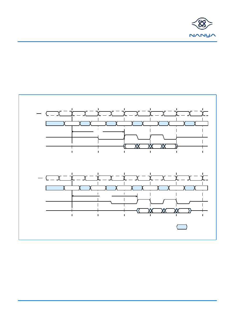
Reads
Subsequent to programming the mode register with CAS latency, burst type, and burst length, Read bursts are initiated with a
Read command.
The starting column and bank addresses are provided with the Read command and Auto Precharge is either enabled or dis-
abled for that burst access. If Auto Precharge is enabled, the row that is accessed starts precharge at the completion of the
burst, provided t
RAS
has been satisfied. For the generic Read commands used in the following illustrations, Auto Precharge is
disabled.
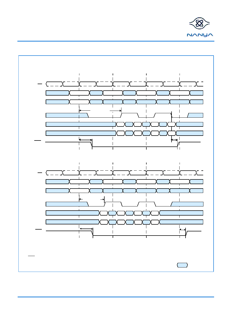
During Read bursts, the valid data-out element from the starting column address is available following the CAS latency after the
Read command. Each subsequent data-out element is valid nominally at the next positive or negative clock edge (i.e. at the
next crossing of CK and CK). The following timing figure entitled "Read Burst: CAS Latencies (Burst Length=4)" illustrates the
general timing for each supported CAS latency setting. DQS is driven by the DDR SDRAM along with output data. The initial low
state on DQS is known as the read preamble; the low state coincident with the last data-out element is known as the read post-
amble. Upon completion of a burst, assuming no other commands have been initiated, the DQs and DQS goes High-Z. Data
from any Read burst may be concatenated with or truncated with data from a subsequent Read command. In either case, a con-
tinuous flow of data can be maintained. The first data element from the new burst follows either the last element of a completed
burst or the last desired data element of a longer burst which is being truncated. The new Read command should be issued x
cycles after the first Read command, where x equals the number of desired data element pairs (pairs are required by the 2n
prefetch architecture). This is shown in timing figure entitled "Consecutive Read Bursts: CAS Latencies (Burst Length =4 or 8)".
A Read command can be initiated on any positive clock cycle following a previous Read command. Nonconsecutive Read data
is shown in timing figure entitled "Non-Consecutive Read Bursts: CAS Latencies (Burst Length = 4)". Full-speed Random Read
Accesses: CAS Latencies (Burst Length = 2, 4 or 8) within a page (or pages) can be performed as shown on page 25.
t
RCD
and t
RRD
Definition
ROW
ACT
NOP
COL
ROW
BA y
BA y
BA x
ACT
NOP
NOP
CK
CK
Command
A0-A12
BA0, BA1
Don't Care
RD/WR
t
RCD
t
RRD
RD/WR
NOP
NOP

NT5DS64M4AT NT5DS64M4AW
NT5DS32M8AT NT5DS32M8AW
256Mb Double Data Rate SDRAM
REV 1.3
08/2002
21
©
NANYA TECHNOLOGY CORP
. All rights reserved.
NANYA TECHNOLOGY CORP. reserves the right to change Products and Specifications without notice.
Read Command
BA
HIGH
CA = column address
BA = bank address
CKE
CS
RAS
CAS
WE
A10
BA0, BA1
Don't Care
CA
x4: A0-A9, A11
x8: A0-A9
EN AP
DIS AP
EN AP = enable Auto Precharge
DIS AP = disable Auto Precharge
CK
CK
NT5DS64M4AT NT5DS64M4AW
NT5DS32M8AT NT5DS32M8AW
256Mb Double Data Rate SDRAM
REV 1.3
08/2002
22
©
NANYA TECHNOLOGY CORP
. All rights reserved.
NANYA TECHNOLOGY CORP. reserves the right to change Products and Specifications without notice.
Read Burst: CAS Latencies (Burst Length = 4)
CAS Latency = 2
NOP
NOP
NOP
NOP
NOP
Read
CK
CK
Command
Address
DQS
DQ
CAS Latency = 2.5
Don't Care
BA a,COL n
DOa-n
CL=2.5
NOP
NOP
NOP
NOP
NOP
Read
CK
CK
Command
Address
DQS
DQ
BA a,COL n
DOa-n
DO a-n = data out from bank a, column n.
3 subsequent elements of data out appear in the programmed order following DO a-n.
Shown with nominal t
AC
, t
DQSCK
, and t
DQSQ
.
CL=2

NT5DS64M4AT NT5DS64M4AW
NT5DS32M8AT NT5DS32M8AW
256Mb Double Data Rate SDRAM
REV 1.3
08/2002
23
©
NANYA TECHNOLOGY CORP
. All rights reserved.
NANYA TECHNOLOGY CORP. reserves the right to change Products and Specifications without notice.
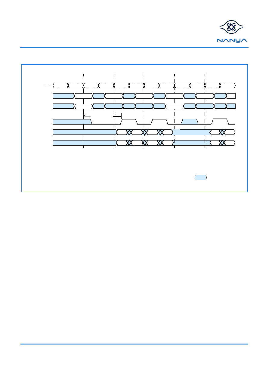
Consecutive Read Bursts: CAS Latencies (Burst Length = 4 or 8)
CAS Latency = 2
NOP
Read
NOP
NOP
NOP
Read
CK
CK
Command
Address
DQS
DQ
CL=2
BAa, COL n
BAa, COL b
Don't Care
DO a-n (or a-b) = data out from bank a, column n (or bank a, column b).
When burst length = 4, the bursts are concatenated.
When burst length = 8, the second burst interrupts the first.
3 subsequent elements of data out appear in the programmed order following DO a-n.
3 (or 7) subsequent elements of data out appear in the programmed order following DO a-b.
Shown with nominal t
AC
, t
DQSCK
, and t
DQSQ
.
CAS Latency = 2.5
NOP
Read
NOP
NOP
NOP
Read
CK
CK
Command
Address
DQS
DQ
CL=2.5
BAa, COL n
BAa,COL b
DOa-n
DOa- n
DOa- b
DOa-b
NT5DS64M4AT NT5DS64M4AW
NT5DS32M8AT NT5DS32M8AW
256Mb Double Data Rate SDRAM
REV 1.3
08/2002
24
©
NANYA TECHNOLOGY CORP
. All rights reserved.
NANYA TECHNOLOGY CORP. reserves the right to change Products and Specifications without notice.
Non-Consecutive Read Bursts: CAS Latencies (Burst Length = 4)
CAS Latency = 2
NOP
NOP
Read
NOP
NOP
Read
CK
CK
Command
Address
DQS
DQ
DO a- n
DOa- b
DO a-n (or a-b) = data out from bank a, column n (or bank a, column b).
3 subsequent elements of data out appear in the programmed order following DO a-n (and following DO a- b).
Shown with nominal t
AC
, t
DQSCK
, and t
DQSQ
.
Don't Care
BAa, COL n
BAa, COL b
CL=2
CAS Latency = 2.5
NOP
NOP
Read
NOP
NOP
Read
DO a- n
DOa- b
BAa, COL n
BAa, COL b
CL=2.5
CK
CK
Command
Address
DQS
DQ
NOP

NT5DS64M4AT NT5DS64M4AW
NT5DS32M8AT NT5DS32M8AW
256Mb Double Data Rate SDRAM
REV 1.3
08/2002
25
©
NANYA TECHNOLOGY CORP
. All rights reserved.
NANYA TECHNOLOGY CORP. reserves the right to change Products and Specifications without notice.
Random Read Accesses: CAS Latencies (Burst Length = 2, 4 or 8)
DOa-n
CAS Latency = 2
Read
Read
Read
NOP
NOP
Read
DOa-b
DOa-n'
DOa-x
DOa-x'
DOa-b'
DOa-g
CK
CK
Command
Address
DQS
DQ
DO a-n, etc. = data out from bank a, column n etc.
n' etc. = odd or even complement of n, etc. (i.e., column address LSB inverted).
Reads are to active rows in any banks.
Shown with nominal t
AC
, t
DQSCK
, and t
DQSQ
.
Don't Care
BAa, COL n
BAa, COL x
BAa, COL b
BAa, COL g
CL=2
DOa-n
CAS Latency = 2.5
Read
Read
Read
NOP
NOP
Read
DOa-b
DOa- n'
DOa-x
DOa-x'
DOa-b'
CK
CK
Command
Address
DQS
DQ
BAa, COL n
BAa, COL x
BAa, COL b
BAa, COL g
CL=2.5

NT5DS64M4AT NT5DS64M4AW
NT5DS32M8AT NT5DS32M8AW
256Mb Double Data Rate SDRAM
REV 1.3
08/2002
26
©
NANYA TECHNOLOGY CORP
. All rights reserved.
NANYA TECHNOLOGY CORP. reserves the right to change Products and Specifications without notice.
Data from any Read burst may be truncated with a Burst Terminate command, as shown in timing figure entitled Terminating a
Read Burst: CAS Latencies (Burst Length = 8) on page 27. The Burst Terminate latency is equal to the read (CAS) latency, i.e.
the Burst Terminate command should be issued x cycles after the Read command, where x equals the number of desired data
element pairs.
Data from any Read burst must be completed or truncated before a subsequent Write command can be issued. If truncation is
necessary, the Burst Terminate command must be used, as shown in timing figure entitled Read to Write: CAS Latencies (Burst
Length = 4 or 8) on page 28. The example is shown for t
DQSS
(min). The t
DQSS
(max) case, not shown here, has a longer bus idle
time. t
DQSS
(min) and t
DQSS
(max) are defined in the section on Writes.
A Read burst may be followed by, or truncated with, a Precharge command to the same bank (provided that Auto Precharge
was not activated). The Precharge command should be issued x cycles after the Read command, where x equals the number of
desired data element pairs (pairs are required by the 2n prefetch architecture). This is shown in timing figure Read to Pre-
charge: CAS Latencies (Burst Length = 4 or 8) on page 29 for Read latencies of 2 and 2.5. Following the Precharge command,
a subsequent command to the same bank cannot be issued until t
RP
is met. Note that part of the row precharge time is hidden
during the access of the last data elements.
In the case of a Read being executed to completion, a Precharge command issued at the optimum time (as described above)
provides the same operation that would result from the same Read burst with Auto Precharge enabled. The disadvantage of the
Precharge command is that it requires that the command and address busses be available at the appropriate time to issue the
command. The advantage of the Precharge command is that it can be used to truncate bursts.
NT5DS64M4AT NT5DS64M4AW
NT5DS32M8AT NT5DS32M8AW
256Mb Double Data Rate SDRAM
REV 1.3
08/2002
27
©
NANYA TECHNOLOGY CORP
. All rights reserved.
NANYA TECHNOLOGY CORP. reserves the right to change Products and Specifications without notice.
Terminating a Read Burst: CAS Latencies (Burst Length = 8)
CAS Latency = 2
NOP
BST
NOP
NOP
NOP
Read
CK
Command
Address
DQS
DQ
DO a-n = data out from bank a, column n.
Cases shown are bursts of 8 terminated after 4 data elements.
3 subsequent elements of data out appear in the programmed order following DO a-n.
Shown with nominal t
AC
, t
DQSCK
, and t
DQSQ
.
DOa-n
Don't Care
CK
BAa, COL n
CL=2
CAS Latency = 2.5
NOP
BST
NOP
NOP
NOP
Read
CK
Command
Address
DQS
DQ
DOa-n
CK
BAa, COL n
CL=2.5
No further output data after this point.
DQS tristated.
No further output data after this point.
DQS tristated.

NT5DS64M4AT NT5DS64M4AW
NT5DS32M8AT NT5DS32M8AW
256Mb Double Data Rate SDRAM
REV 1.3
08/2002
28
©
NANYA TECHNOLOGY CORP
. All rights reserved.
NANYA TECHNOLOGY CORP. reserves the right to change Products and Specifications without notice.
Read to Write: CAS Latencies (Burst Length = 4 or 8)
CAS Latency = 2
BST
NOP
Write
NOP
NOP
Read
DI a-b
CK
CK
Command
Address
DQS
DQ
DM
DOa-n
DO a-n = data out from bank a, column n
1 subsequent elements of data out appear in the programmed order following DO a-n.
Data In elements are applied following Dl a-b in the programmed order, according to burst length.
Don't Care
BAa, COL n
BAa, COL b
CL=2
t
DQSS
(min)
CAS Latency = 2.5
BST
NOP
NOP
Write
NOP
Read
CK
CK
Command
Address
DQS
DQ
DM
DOa-n
BAa, COL n
BAa, COL b
CL=2.5
t
DQSS
(min)
Dla-b
Shown with nominal t
AC
, t
DQSCK
, and t
DQSQ
.
.
DI a-b = data in to bank a, column b
NT5DS64M4AT NT5DS64M4AW
NT5DS32M8AT NT5DS32M8AW
256Mb Double Data Rate SDRAM
REV 1.3
08/2002
29
©
NANYA TECHNOLOGY CORP
. All rights reserved.
NANYA TECHNOLOGY CORP. reserves the right to change Products and Specifications without notice.
Read to Precharge: CAS Latencies (Burst Length = 4 or 8)
CAS Latency = 2
NOP
PRE
NOP
NOP
ACT
Read
CK
CK
Command
Address
DQS
DQ
DOa-n
DO a-n = data out from bank a, column n.
Cases shown are either uninterrupted bursts of 4 or interrupted bursts of 8.
3 subsequent elements of data out appear in the programmed order following DO a-n.
Shown with nominal t
AC
, t
DQSCK
, and t
DQSQ
.
Don't Care
BA a, COL n
BA a or all
BA a, ROW
CL=2.5
CAS Latency = 2.5
NOP
PRE
NOP
NOP
ACT
Read
CK
CK
Command
Address
DQS
DQ
DOa-n
t
R P
BA a, COL n
BA a or all
BA a, ROW
CL=2
t
R P

NT5DS64M4AT NT5DS64M4AW
NT5DS32M8AT NT5DS32M8AW
256Mb Double Data Rate SDRAM
REV 1.3
08/2002
30
©
NANYA TECHNOLOGY CORP
. All rights reserved.
NANYA TECHNOLOGY CORP. reserves the right to change Products and Specifications without notice.
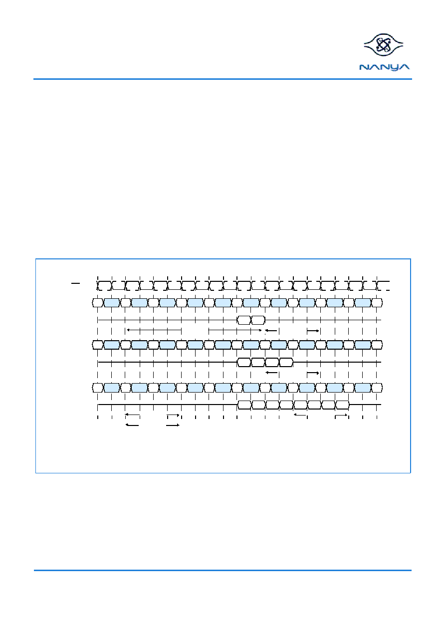
Writes
Write bursts are initiated with a Write command, as shown in timing figure Write Command on page 31.
The starting column and bank addresses are provided with the Write command, and Auto Precharge is either enabled or dis-
abled for that access. If Auto Precharge is enabled, the row being accessed is precharged at the completion of the burst. For
the generic Write commands used in the following illustrations, Auto Precharge is disabled.
During Write bursts, the first valid data-in element is registered on the first rising edge of DQS following the write command, and
subsequent data elements are registered on successive edges of DQS. The Low state on DQS between the Write command
and the first rising edge is known as the write preamble; the Low state on DQS following the last data-in element is known as
the write postamble. The time between the Write command and the first corresponding rising edge of DQS (t
DQSS
) is specified
with a relatively wide range (from 75% to 125% of one clock cycle), so most of the Write diagrams that follow are drawn for the
two extreme cases (i.e. t
DQSS
(min) and t
DQSS
(max)). Timing figure Write Burst (Burst Length = 4) on page 32 shows the two
extremes of t
DQSS
for a burst of four. Upon completion of a burst, assuming no other commands have been initiated, the DQs
and DQS enters High-Z and any additional input data is ignored.
Data for any Write burst may be concatenated with or truncated with a subsequent Write command. In either case, a continuous
flow of input data can be maintained. The new Write command can be issued on any positive edge of clock following the previ-
ous Write command. The first data element from the new burst is applied after either the last element of a completed burst or
the last desired data element of a longer burst which is being truncated. The new Write command should be issued x cycles
after the first Write command, where x equals the number of desired data element pairs (pairs are required by the 2n prefetch
architecture). Timing figure Write to Write (Burst Length = 4) on page 33 shows concatenated bursts of 4. An example of non-
consecutive Writes is shown in timing figure Write to Write: Max DQSS, Non-Consecutive (Burst Length = 4) on page 34. Full-
speed random write accesses within a page or pages can be performed as shown in timing figure Random Write Cycles (Burst
Length = 2, 4 or 8) on page 35. Data for any Write burst may be followed by a subsequent Read command. To follow a Write
without truncating the write burst, t
WTR
(Write to Read) should be met as shown in timing figure Write to Read: Non-Interrupting
(CAS Latency = 2; Burst Length = 4) on page 36.
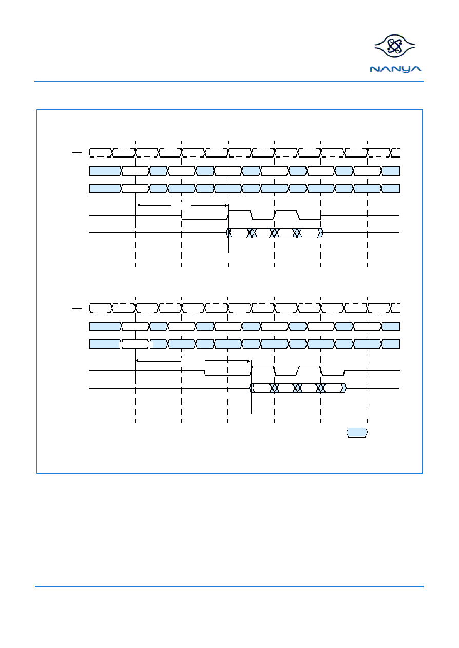
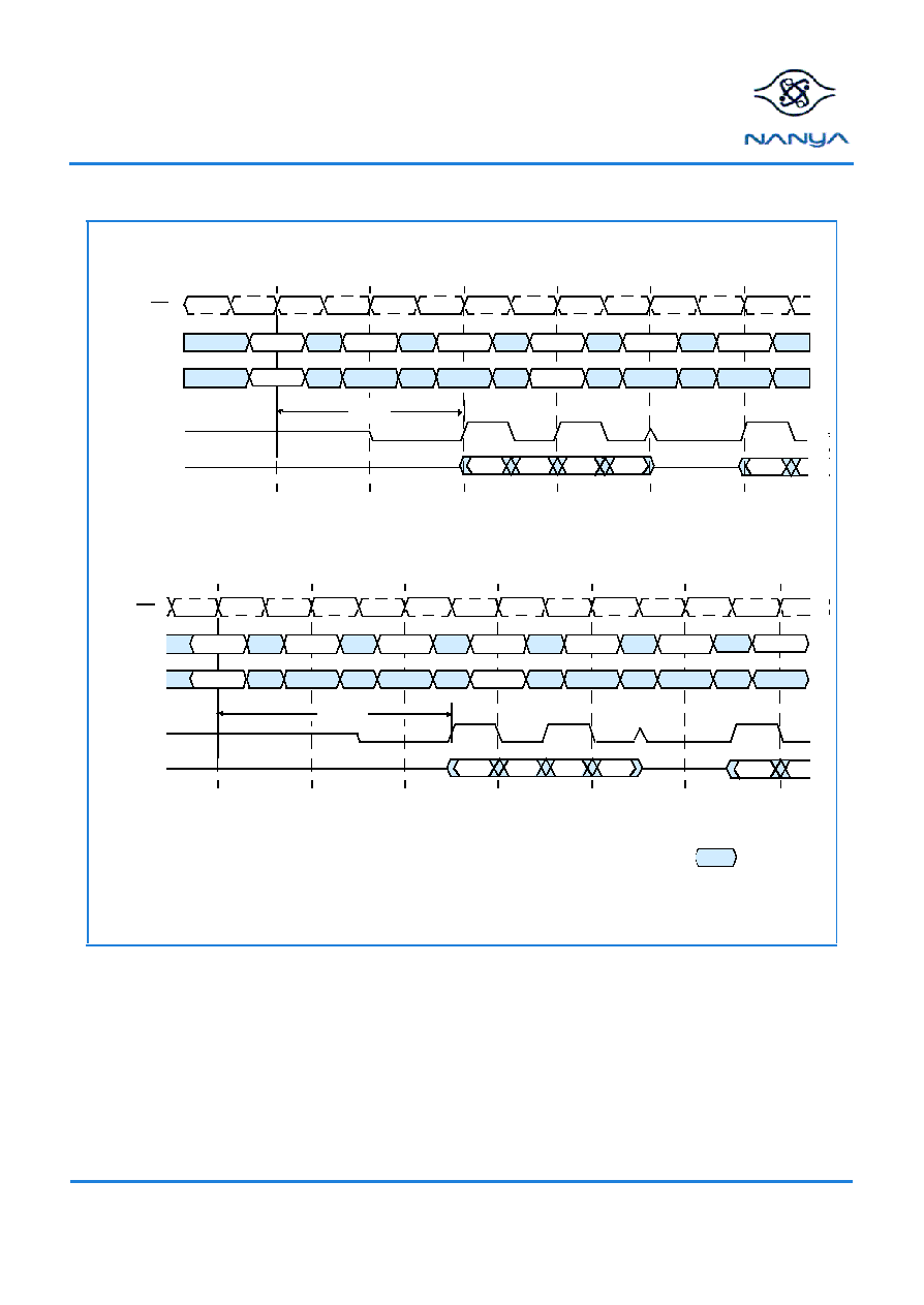
Data for any Write burst may be truncated by a subsequent (interrupting) Read command. This is illustrated in timing figures
"Write to Read: Interrupting (CAS Latency =2; Burst Length = 8)", "Write to Read: Minimum D
QSS
, Odd Number of Data (3 bit
Write), Interrupting (CAS Latency = 2; Burst Length = 8)", and "Write to Read: Nominal D
QSS
, Interrupting (CAS Latency = 2;
Burst Length = 8)". Note that only the data-in pairs that are registered prior to the t
WTR
period are written to the internal array,
and any subsequent data-in must be masked with DM, as shown in the diagrams noted previously.
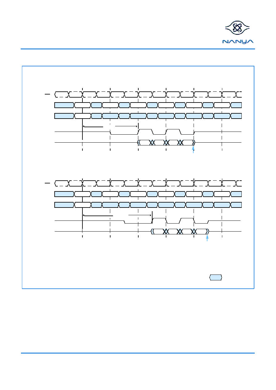
Data for any Write burst may be followed by a subsequent Precharge command. To follow a Write without truncating the write
burst, t
WR
should be met as shown in timing figure Write to Precharge: Non-Interrupting (Burst Length = 4) on page 40.
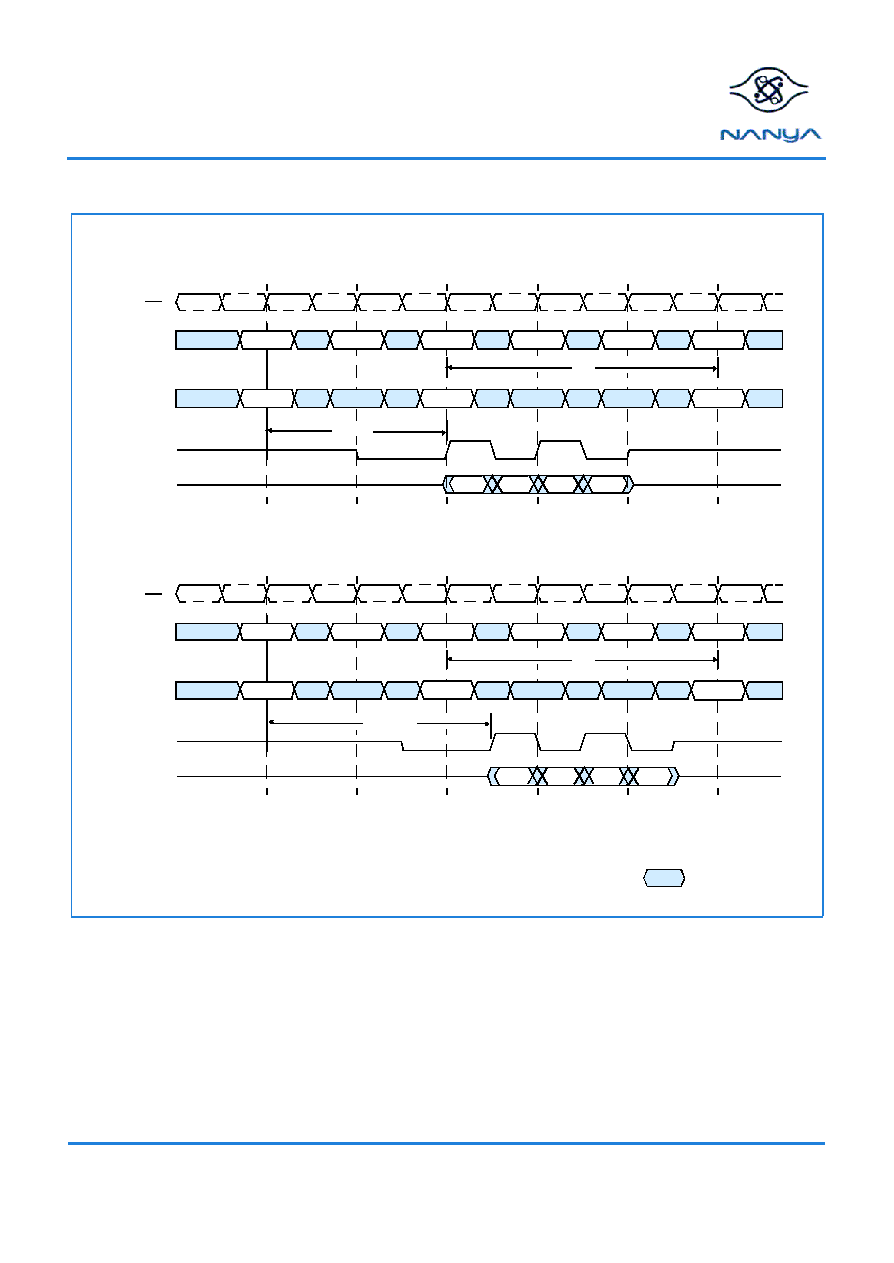
Data for any Write burst may be truncated by a subsequent Precharge command, as shown in timing figures Write to Pre-
charge: Interrupting (Burst Length = 4 or 8) on page 41 to Write to Precharge: Nominal DQSS (2 bit Write), Interrupting (Burst
Length = 4 or 8) on page 43. Note that only the data-in pairs that are registered prior to the t
WR
period are written to the internal
array, and any subsequent data in should be masked with DM. Following the Precharge command, a subsequent command to
the same bank cannot be issued until t
RP
is met.
In the case of a Write burst being executed to completion, a Precharge command issued at the optimum time (as described
above) provides the same operation that would result from the same burst with Auto Precharge. The disadvantage of the Pre-
charge command is that it requires that the command and address busses be available at the appropriate time to issue the com-
mand. The advantage of the Precharge command is that it can be used to truncate bursts.
NT5DS64M4AT NT5DS64M4AW
NT5DS32M8AT NT5DS32M8AW
256Mb Double Data Rate SDRAM
REV 1.3
08/2002
31
©
NANYA TECHNOLOGY CORP
. All rights reserved.
NANYA TECHNOLOGY CORP. reserves the right to change Products and Specifications without notice.
Write Command
BA
HIGH
CA = column address
BA = bank address
CKE
CS
RAS
CAS
WE
A10
BA0, BA1
Don't Care
CA
x4: A0-A9, A11
x8: A0-A9
EN AP
DIS AP
EN AP = enable Auto Precharge
DIS AP = disable Auto Precharge
CK
CK
NT5DS64M4AT NT5DS64M4AW
NT5DS32M8AT NT5DS32M8AW
256Mb Double Data Rate SDRAM
REV 1.3
08/2002
32
©
NANYA TECHNOLOGY CORP
. All rights reserved.
NANYA TECHNOLOGY CORP. reserves the right to change Products and Specifications without notice.
Write Burst (Burst Length = 4)
T1
T2
T3
T4
t
DQSS
(max)
NOP
NOP
NOP
Write
DI a-b = data in for bank a, column b.
3 subsequent elements of data in are applied in the programmed order following DI a- b.
A non-interrupted burst is shown.
A10 is Low with the Write command (Auto Precharge is disabled).
CK
CK
Command
Address
DQS
DQ
DM
Don't Care
Maximum D
QSS
BA a, COL b
T1
T2
T3
T4
t
DQSS
(min)
NOP
NOP
NOP
Write
CK
CK
Command
Address
DQS
Minimum D
QSS
BA a, COL b
DQ
DM
Dla-b
Dla-b
QFC
t
QCSW
(max)
t
QCHW
(min)
(Optional)
QFC
t
QCSW
(max)
t
QCHW
(max)
QFC is an open drain driver. Its output high level is achieved through an externally connected pull up resistor connected to V
DDQ
.

NT5DS64M4AT NT5DS64M4AW
NT5DS32M8AT NT5DS32M8AW
256Mb Double Data Rate SDRAM
REV 1.3
08/2002
33
©
NANYA TECHNOLOGY CORP
. All rights reserved.
NANYA TECHNOLOGY CORP. reserves the right to change Products and Specifications without notice.
Write to Write (Burst Length = 4)
T1
T2
T3
T4
T5
T6
t
DQSS
(max)
Maximum D
QSS
NOP
Write
NOP
NOP
NOP
Write
DI a-b = data in for bank a, column b, etc.
3 subsequent elements of data in are applied in the programmed order following DI a-b.
3 subsequent elements of data in are applied in the programmed order following DI a-n.
A non-interrupted burst is shown.
Each Write command may be to any bank.
CK
CK
Command
Address
DQS
DQ
DM
Don't Care
T1
T2
T3
T4
T5
T6
Minimum D
QSS
NOP
Write
NOP
NOP
NOP
Write
CK
CK
Command
Address
DQS
DQ
DM
BAa, COL b
BAa, COL n
BA, COL b
BA, COL n
t
DQSS
(min)
DI a-b
DI a-n
DI a-b
DI a-n
NT5DS64M4AT NT5DS64M4AW
NT5DS32M8AT NT5DS32M8AW
256Mb Double Data Rate SDRAM
REV 1.3
08/2002
34
©
NANYA TECHNOLOGY CORP
. All rights reserved.
NANYA TECHNOLOGY CORP. reserves the right to change Products and Specifications without notice.
Write to Write: Max DQSS, Non-Consecutive (Burst Length = 4)
T1
T2
T3
T4
T5
t
DQSS
(max)
NOP
NOP
Write
NOP
Write
DI a-b, etc. = data in for bank a, column b, etc.
3 subsequent elements of data in are applied in the programmed order following DI a-b.
3 subsequent elements of data in are applied in the programmed order following DI a-n.
A non-interrupted burst is shown.
Each Write command may be to any bank.
CK
CK
Command
Address
DQS
DQ
DM
Don't Care
BAa, COL b
BAa, COL n
DI a-b
DI a-n

NT5DS64M4AT NT5DS64M4AW
NT5DS32M8AT NT5DS32M8AW
256Mb Double Data Rate SDRAM
REV 1.3
08/2002
35
©
NANYA TECHNOLOGY CORP
. All rights reserved.
NANYA TECHNOLOGY CORP. reserves the right to change Products and Specifications without notice.
Random Write Cycles (Burst Length = 2, 4 or 8)
T1
T2
T3
T4
T5
t
DQSS
(max)
Maximum D
QSS
Write
Write
Write
Write
Write
DI a-b
DI a-n
DI a-b, etc. = data in for bank a, column b, etc.
b', etc. = odd or even complement of b, etc. (i.e., column address LSB inverted).
Each Write command may be to any bank.
DI a-b'
DI a-x
DI a-x'
DI a-n'
DI a-a
DI a-a'
CK
CK
Command
Address
DQS
DQ
DM
Don't Care
BAa, COL b
BAa, COL x
BAa, COL n
BAa, COL a
BAa, COL g
T1
T2
T3
T4
T5
Minimum D
QSS
Write
Write
Write
Write
Write
DI a-b
DI a-n
DI a-b'
DI a-x
DI a-x'
DI a-n'
DI a-a
DI a-a'
CK
CK
Command
Address
DQS
DQ
DM
BAa, COL b
BAa, COL x
BAa, COL n
BAa, COL a
BAa, COL g
t
DQSS
(min)
DI a-g

NT5DS64M4AT NT5DS64M4AW
NT5DS32M8AT NT5DS32M8AW
256Mb Double Data Rate SDRAM
REV 1.3
08/2002
36
©
NANYA TECHNOLOGY CORP
. All rights reserved.
NANYA TECHNOLOGY CORP. reserves the right to change Products and Specifications without notice.
Write to Read: Non-Interrupting (CAS Latency = 2; Burst Length = 4)
CL = 2
T1
T2
T3
T4
T5
T6
t
WTR
NOP
NOP
NOP
Read
Write
DI a- b
NOP
DI a-b = data in for bank a, column b.
3 subsequent elements of data in are applied in the programmed order following DI a-b.
A non-interrupted burst is shown.
t
WTR
is referenced from the first positive CK edge after the last data in pair.
A10 is Low with the Write command (Auto Precharge is disabled).
The Read and Write commands may be to any bank.
CK
CK
Command
Address
DQS
DQ
DM
Don't Care
Maximum D
QSS
BAa, COL b
BAa, COL n
T1
T2
T3
T4
T5
T6
t
WTR
NOP
NOP
NOP
Read
Write
NOP
CK
CK
Command
Address
Minimum D
QSS
BAa, COL b
BAa, COL n
t
DQSS
(max)
DI a- b
DQS
DQ
DM
t
DQSS
(min)
CL = 2

NT5DS64M4AT NT5DS64M4AW
NT5DS32M8AT NT5DS32M8AW
256Mb Double Data Rate SDRAM
REV 1.3
08/2002
37
©
NANYA TECHNOLOGY CORP
. All rights reserved.
NANYA TECHNOLOGY CORP. reserves the right to change Products and Specifications without notice.
Write to Read: Interrupting (CAS Latency = 2; Burst Length = 8)
T1
T2
T3
T4
T5
T6
t
DQSS
(max)
Maximum D
QSS
NOP
NOP
NOP
Read
Write
NOP
DI a-b = data in for bank a, column b.
An interrupted burst is shown, 4 data elements are written.
3 subsequent elements of data in are applied in the programmed order following DI a-b.
t
WTR
is referenced from the first positive CK edge after the last data in pair.
The Read command masks the last 2 data elements in the burst.
A10 is Low with the Write command (Auto Precharge is disabled).
The Read and Write commands are not necessarily to the same bank.
DIa- b
CK
CK
Command
Address
DQS
DQ
DM
Don't Care
BAa, COL b
BAa, COL n
t
W T R
CL = 2
T1
T2
T3
T4
T5
T6
Minimum D
QSS
NOP
NOP
NOP
Read
Write
NOP
CK
CK
Command
Address
BAa, COL b
BAa, COL n
t
WTR
DI a-b
DQS
DQ
DM
CL = 2
t
DQSS
(min)
1 = These bits are incorrectly written into the memory array if DM is low.
1
1
1
1

NT5DS64M4AT NT5DS64M4AW
NT5DS32M8AT NT5DS32M8AW
256Mb Double Data Rate SDRAM
REV 1.3
08/2002
38
©
NANYA TECHNOLOGY CORP
. All rights reserved.
NANYA TECHNOLOGY CORP. reserves the right to change Products and Specifications without notice.
Write to Read: Minimum DQSS, Odd Number of Data (3 bit Write), Interrupting (CAS
Latency = 2; Burst Length = 8)
DI a-b = data in for bank a, column b.
An interrupted burst is shown, 3 data elements are written.
2 subsequent elements of data in are applied in the programmed order following DI a-b .
t
WTR
is referenced from the first positive CK edge after the last desired data in pair (not the last desired data in element)
The Read command masks the last 2 data elements in the burst.
A10 is Low with the Write command (Auto Precharge is disabled).
The Read and Write commands are not necessarily to the same bank.
Don't Care
T1
T2
T3
T4
T5
T6
NOP
NOP
NOP
Read
Write
NOP
CK
CK
Command
Address
BAa, COL b
BAa, COL n
t
W T R
DI a-b
DQS
DQ
CL = 2
t
DQSS
(min)
DM
1
2
2
1 = This bit is correctly written into the memory array if DM is low.
2 = These bits are incorrectly written into the memory array if DM is low.

NT5DS64M4AT NT5DS64M4AW
NT5DS32M8AT NT5DS32M8AW
256Mb Double Data Rate SDRAM
REV 1.3
08/2002
39
©
NANYA TECHNOLOGY CORP
. All rights reserved.
NANYA TECHNOLOGY CORP. reserves the right to change Products and Specifications without notice.
Write to Read: Nominal DQSS, Interrupting (CAS Latency = 2; Burst Length = 8)
T1
T2
T3
T4
T5
T6
t
DQSS
(nom)
NOP
NOP
NOP
Read
Write
NOP
DI a-b = data in for bank a, column b.
An interrupted burst is shown, 4 data elements are written.
3 subsequent elements of data in are applied in the programmed order following DI a-b.
t
WTR
is referenced from the first positive CK edge after the last desired data in pair.
The Read command masks the last 2 data elements in the burst.
A10 is Low with the Write command (Auto Precharge is disabled).
The Read and Write commands are not necessarily to the same bank.
DI a- b
CK
CK
Command
Address
DQS
DQ
DM
Don't Care
BAa, COL b
BAa, COL n
t
WTR
CL = 2
1 = These bits are incorrectly written into the memory array if DM is low.
1
1
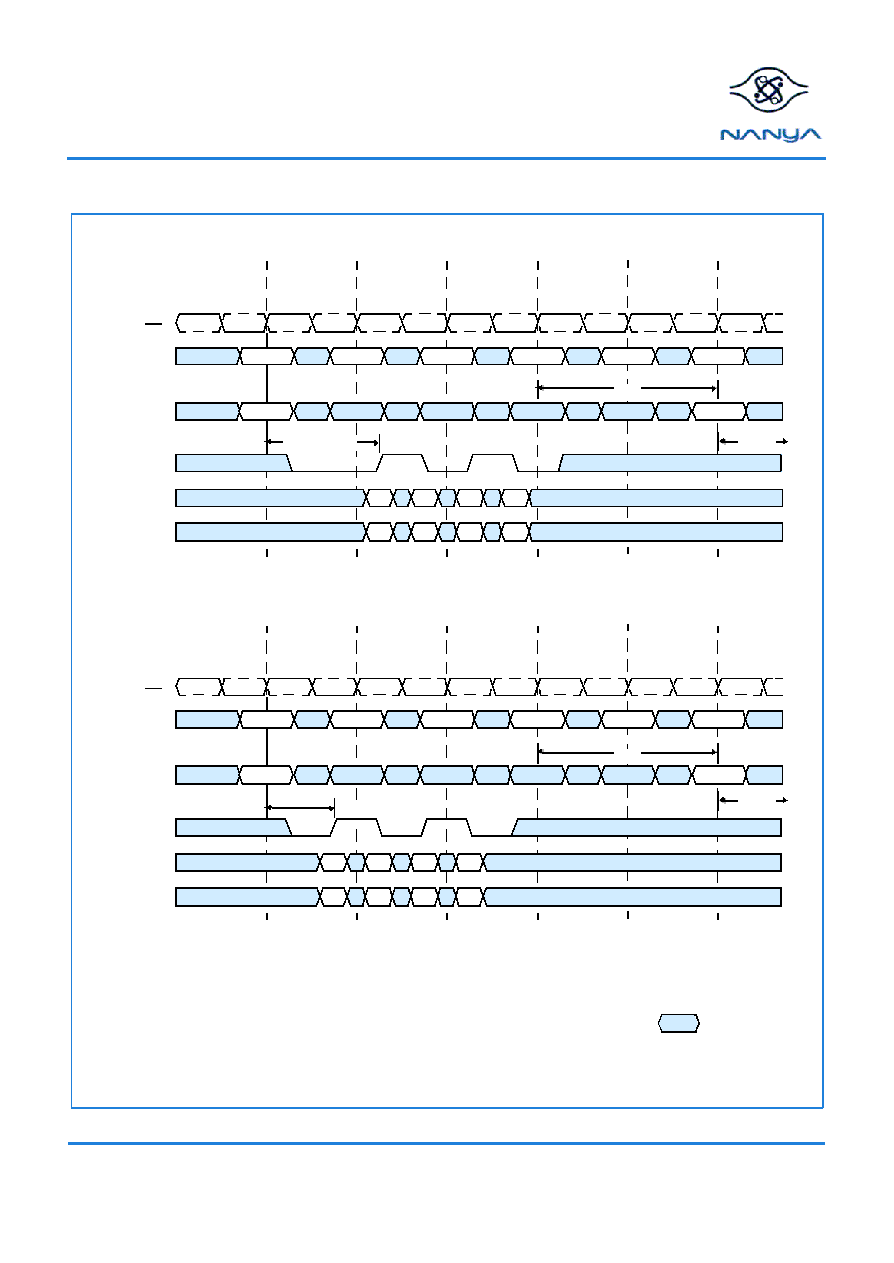
NT5DS64M4AT NT5DS64M4AW
NT5DS32M8AT NT5DS32M8AW
256Mb Double Data Rate SDRAM
REV 1.3
08/2002
40
©
NANYA TECHNOLOGY CORP
. All rights reserved.
NANYA TECHNOLOGY CORP. reserves the right to change Products and Specifications without notice.
Write to Precharge: Non-Interrupting (Burst Length = 4)
T1
T2
T3
T4
T5
T6
t
DQSS
(max)
NOP
NOP
NOP
NOP
Write
DI a-b
PRE
DI a-b = data in for bank a, column b.
3 subsequent elements of data in are applied in the programmed order following DI a-b.
A non-interrupted burst is shown.
t
WR
is referenced from the first positive CK edge after the last data in pair.
A10 is Low with the Write command (Auto Precharge is disabled).
CK
CK
Command
Address
DQS
DQ
DM
Don't Care
BA a, COL b
BA (a or all)
t
WR
Maximum D
QSS
T1
T2
T3
T4
T5
T6
NOP
NOP
NOP
NOP
Write
PRE
CK
CK
Command
Address
BA a, COL b
BA (a or all)
t
WR
Minimum D
QSS
DI a-b
DQS
DQ
DM
t
DQSS
(min)
t
RP
t
RP
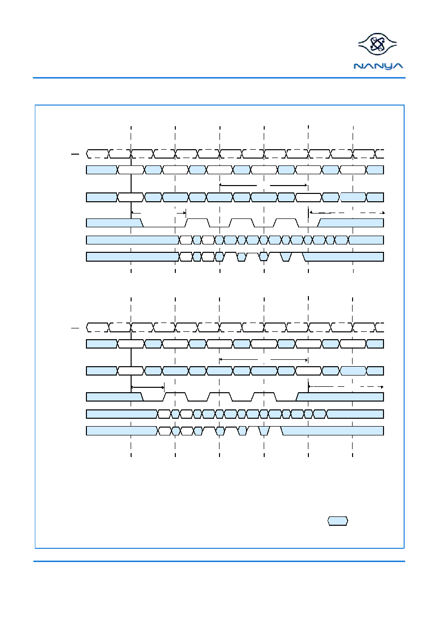
NT5DS64M4AT NT5DS64M4AW
NT5DS32M8AT NT5DS32M8AW
256Mb Double Data Rate SDRAM
REV 1.3
08/2002
41
©
NANYA TECHNOLOGY CORP
. All rights reserved.
NANYA TECHNOLOGY CORP. reserves the right to change Products and Specifications without notice.
Write to Precharge: Interrupting (Burst Length = 4 or 8)
DI a- b = data in for bank a, column b.
An interrupted burst is shown, 2 data elements are written.
1 subsequent element of data in is applied in the programmed order following DI a-b.
t
WR
is referenced from the first positive CK edge after the last desired data in pair.
The Precharge command masks the last 2 data elements in the burst, for burst length = 8.
A10 is Low with the Write command (Auto Precharge is disabled).
1 = Can be don't care for programmed burst length of 4.
2 = For programmed burst length of 4, DQS becomes don't care at this point.
Don't Care
T1
T2
T3
T4
T5
T6
NOP
NOP
NOP
PRE
Write
NOP
CK
CK
Command
Address
Maximum D
QSS
DI a-b
1
1
2
DQS
DQ
DM
t
DQSS
(max)
t
R P
T1
T2
T3
T4
T5
T6
NOP
NOP
NOP
PRE
Write
NOP
CK
CK
Command
Address
BA a, COL b
BA (a or all)
Minimum D
QSS
t
WR
t
R P
DI a-b
1
1
DQS
DQ
DM
t
DQSS
(min)
2
BA a, COL b
BA (a or all)
t
WR
3 = These bits are incorrectly written into the memory array if DM is low.
3
3
3
3
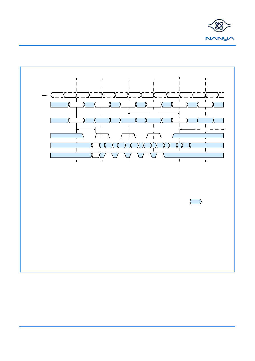
NT5DS64M4AT NT5DS64M4AW
NT5DS32M8AT NT5DS32M8AW
256Mb Double Data Rate SDRAM
REV 1.3
08/2002
42
©
NANYA TECHNOLOGY CORP
. All rights reserved.
NANYA TECHNOLOGY CORP. reserves the right to change Products and Specifications without notice.
Write to Precharge: Minimum DQSS, Odd Number of Data (1 bit Write), Interrupting
(Burst Length = 4 or 8)
DI a-b = data in for bank a, column b.
An interrupted burst is shown, 1 data element is written.
t
WR
is referenced from the first positive CK edge after the last desired data in pair.
The Precharge command masks the last 2 data elements in the burst.
A10 is Low with the Write command (Auto Precharge is disabled).
1 = Can be don't care for programmed burst length of 4.
2 = For programmed burst length of 4, DQS becomes don't care at this point.
Don't Care
T1
T2
T3
T4
T5
T6
NOP
NOP
NOP
PRE
Write
NOP
CK
CK
Command
Address
BA a, COL b
BA (a or all)
t
WR
t
RP
DI a-b
DQS
DQ
t
DQSS
(min)
2
1
1
DM
3
4
4
3 = This bit is correctly written into the memory array if DM is low.
4 = These bits are incorrectly written into the memory array if DM is low.

NT5DS64M4AT NT5DS64M4AW
NT5DS32M8AT NT5DS32M8AW
256Mb Double Data Rate SDRAM
REV 1.3
08/2002
43
©
NANYA TECHNOLOGY CORP
. All rights reserved.
NANYA TECHNOLOGY CORP. reserves the right to change Products and Specifications without notice.
Write to Precharge: Nominal DQSS (2 bit Write), Interrupting (Burst Length = 4 or 8)
DI a-b = Data In for bank a, column b.
An interrupted burst is shown, 2 data elements are written.
1 subsequent element of data in is applied in the programmed order following DI a-b.
t
WR
is referenced from the first positive CK edge after the last desired data in pair.
The Precharge command masks the last 2 data elements in the burst.
A10 is Low with the Write command (Auto Precharge is disabled).
1 = Can be don't care for programmed burst length of 4.
2 = For programmed burst length of 4, DQS becomes don't care at this point.
Don't Care
T1
T2
T3
T4
T5
T6
NOP
NOP
NOP
PRE
Write
NOP
CK
CK
Command
Address
BA a, COL b
BA (a or all)
t
RP
t
DQSS
(nom)
DI a-b
1
2
DQS
DQ
DM
1
t
WR
3
3
3 = These bits are incorrectly written into the memory array if DM is low.

NT5DS64M4AT NT5DS64M4AW
NT5DS32M8AT NT5DS32M8AW
256Mb Double Data Rate SDRAM
REV 1.3
08/2002
44
©
NANYA TECHNOLOGY CORP
. All rights reserved.
NANYA TECHNOLOGY CORP. reserves the right to change Products and Specifications without notice.
Precharge
The Precharge command is used to deactivate the open row in a particular bank or the open row in all banks. The
bank(s) is available for a subsequent row access some specified time (t
RP
) after the Precharge command is
issued. Input A10 determines whether one or all banks are to be precharged, and in the case where only one bank
is to be precharged, inputs BA0, BA1 select the bank. When all banks are to be precharged, inputs BA0, BA1 are
treated as "Don't Care." Once a bank has been precharged, it is in the idle state and must be activated prior to any
Read or Write commands being issued to that bank.
Precharge Command
BA
HIGH
BA = bank address
CK
CK
CKE
CS
RAS
CAS
WE
A10
BA0, BA1
Don't Care
All Banks
One Bank
(if A10 is Low, otherwise Don't Care).
A0-A9, A11, A12
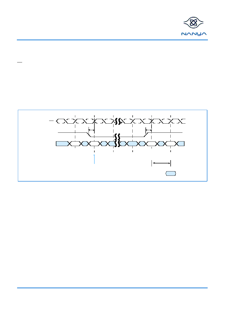
NT5DS64M4AT NT5DS64M4AW
NT5DS32M8AT NT5DS32M8AW
256Mb Double Data Rate SDRAM
REV 1.3
08/2002
45
©
NANYA TECHNOLOGY CORP
. All rights reserved.
NANYA TECHNOLOGY CORP. reserves the right to change Products and Specifications without notice.
Power Down
Power Down mode is entered when CKE is registered low (no accesses can be in progress). If power down occurs when all
banks are idle, this mode is referred to as Precharge Power Down; if power down occurs when there is a row active in any bank,
this mode is referred to as Active Power Down. Entering Power Down deactivates the input and output buffers, excluding CK,
CK and CKE. The DLL is still running in Power Down mode, so for maximum power savings, the user has the option of disabling
the DLL prior to entering Power Down. In that case, the DLL must be enabled after exiting Power Down, and 200 clock cycles
must occur before a Read command can be issued. In Power Down mode, CKE Low and a stable clock signal must be main-
tained at the inputs of the DDR SDRAM, and all other input signals are "Don't Care". However, power down duration is limited
by the refresh requirements of the device, so in most applications, the self refresh mode is preferred over the DLL-disabled
Power Down mode.
The Power Down state is synchronously exited when CKE is registered high (along with a Nop or Deselect command). A valid,
executable command may be applied one clock cycle later.
Power Down
t
IS
t
IS
CK
CK
CKE
Command
No column
access in
progress
VALID
NOP
VALID
Don't Care
Exit
power down
mode
Enter Power Down mode
(Burst Read or Write operation
must not be in progress)
NOP
t
XARD

NT5DS64M4AT NT5DS64M4AW
NT5DS32M8AT NT5DS32M8AW
256Mb Double Data Rate SDRAM
REV 1.3
08/2002
46
©
NANYA TECHNOLOGY CORP
. All rights reserved.
NANYA TECHNOLOGY CORP. reserves the right to change Products and Specifications without notice.
Truth Table 2: Clock Enable (CKE)
1. CKE n is the logic state of CKE at clock edge n: CKE n-1 was the state of CKE at the previous clock edge.
2. Current state is the state of the DDR SDRAM immediately prior to clock edge n.
3. Command n is the command registered at clock edge n, and action n is a result of command n.
4. All states and sequences not shown are illegal or reserved.
Current State
CKE n-1
CKEn
Command n
Action n
Notes
Previous
Cycle
Current
Cycle
Self Refresh
L
L
X
Maintain Self-Refresh
Self Refresh
L
H
Deselect or NOP
Exit Self-Refresh
1
Power Down
L
L
X
Maintain Power Down
Power Down
L
H
Deselect or NOP
Exit Power Down
All Banks Idle
H
L
Deselect or NOP
Precharge Power Down Entry
All Banks Idle
H
L
Auto Refresh
Self Refresh Entry
Bank(s) Active
H
L
Deselect or NOP
Active Power Down Entry
H
H
See "Truth Table 3: Current State
Bank n - Command to Bank n (Same
Bank) " on page 47
1. Deselect or NOP commands should be issued on any clock edges occurring during the Self Refresh Exit (t
XSNR
) period. A minimum of
200 clock cycles are needed before applying a read command to allow the DLL to lock to the input clock.

NT5DS64M4AT NT5DS64M4AW
NT5DS32M8AT NT5DS32M8AW
256Mb Double Data Rate SDRAM
REV 1.3
08/2002
47
©
NANYA TECHNOLOGY CORP
. All rights reserved.
NANYA TECHNOLOGY CORP. reserves the right to change Products and Specifications without notice.
Truth Table 3: Current State Bank n - Command to Bank n (Same Bank)
Current State
CS
RAS
CAS
WE
Command
Action
Notes
Any
H
X
X
X
Deselect
NOP. Continue previous operation
1-6
L
H
H
H
No Operation
NOP. Continue previous operation
1-6
Idle
L
L
H
H
Active
Select and activate row
1-6
L
L
L
H
Auto Refresh
1-7
L
L
L
L
Mode Register Set
1-7
Row Active
L
H
L
H
Read
Select column and start Read burst
1-6, 10
L
H
L
L
Write
Select column and start Write burst
1-6, 10
L
L
H
L
Precharge
Deactivate row in bank(s)
1-6, 8
Read
(Auto Precharge
Disabled)
L
H
L
H
Read
Select column and start new Read burst
1-6, 10
L
L
H
L
Precharge
Truncate Read burst, start Precharge
1-6, 8
L
H
H
L
Burst Terminate
Burst Terminate
1-6, 9
Write
(Auto Precharge
Disabled)
L
H
L
H
Read
Select column and start Read burst
1-6, 10, 11
L
H
L
L
Write
Select column and start Write burst
1-6, 10
L
L
H
L
Precharge
Truncate Write burst, start Precharge
1-6, 8, 11
1. This table applies when CKE n-1 was high and CKE n is high (see Truth Table 2: Clock Enable (CKE) and after t
XSNR /
t
XSRD
has been
met (if the previous state was self refresh).
2. This table is bank-specific, except where noted, i.e., the current state is for a specific bank and the commands shown are those allowed
to be issued to that bank when in that state. Exceptions are covered in the notes below.
3. Current state definitions:
Idle:
The bank has been precharged, and t
RP
has been met.
Row Active:
A row in the bank has been activated, and t
RCD
has been met. No data bursts/accesses and no register accesses are in
progress.
Read:
A Read burst has been initiated, with Auto Precharge disabled, and has not yet terminated or been terminated.
Write:
A Write burst has been initiated, with Auto Precharge disabled, and has not yet terminated or been terminated.
4. The following states must not be interrupted by a command issued to the same bank.
Precharging:
Starts with registration of a Precharge command and ends when t
R P
is met. Once t
RP
is met, the bank is in the idle
state.
Row Activating: Starts with registration of an Active command and ends when t
RCD
is met. Once t
RCD
is met, the bank is in the "row
active" state.
Read w/Auto Precharge Enabled: Starts with registration of a Read command with Auto Precharge enabled and ends when t
RP
has been
met. Once t
RP
is met, the bank is in the idle state.
Write w/Auto Precharge Enabled: Starts with registration of a Write command with Auto Precharge enabled and ends when t
RP
has been
met. Once t
RP
is met, the bank is in the idle state.
Deselect or NOP commands, or allowable commands to the other bank should be issued on any clock edge occurring during these
states. Allowable commands to the other bank are determined by its current state and according to Truth Table 4.
5. The following states must not be interrupted by any executable command; Deselect or NOP commands must be applied on each positive
clock edge during these states.
Refreshing:
Starts with registration of an Auto Refresh command and ends when t
RFC
is met. Once t
RFC
is met, the DDR SDRAM is
in the "all banks idle" state.
Accessing Mode Register: Starts with registration of a Mode Register Set command and ends when t
MRD
has been met. Once t
MRD
is
met, the DDR SDRAM is in the "all banks idle" state.
Precharging All: Starts with registration of a Precharge All command and ends when t
RP
is met. Once t
RP
is met, all banks is in the idle
state.
6. All states and sequences not shown are illegal or reserved.
7. Not bank-specific; requires that all banks are idle.
8. May or may not be bank-specific; if all/any banks are to be precharged, all/any must be in a valid state for precharging.
9. Not bank-specific; Burst terminate affects the most recent Read burst, regardless of bank.
10. Reads or Writes listed in the Command/Action column include Reads or Writes with Auto Precharge enabled and Reads or Writes with
Auto Precharge disabled.
11. Requires appropriate DM masking.

NT5DS64M4AT NT5DS64M4AW
NT5DS32M8AT NT5DS32M8AW
256Mb Double Data Rate SDRAM
REV 1.3
08/2002
48
©
NANYA TECHNOLOGY CORP
. All rights reserved.
NANYA TECHNOLOGY CORP. reserves the right to change Products and Specifications without notice.
Truth Table 4: Current State Bank n - Command to Bank m (Different bank)
(Part 1 of 2)
Current State
CS
RAS
CAS
WE
Command
Action
Notes
Any
H
X
X
X
Deselect
NOP/continue previous operation
1-6
L
H
H
H
No Operation
NOP/continue previous operation
1-6
Idle
X
X
X
X
Any Command Otherwise
Allowed to Bank m
1-6
Row Activating,
Active, or
Precharging
L
L
H
H
Active
Select and activate row
1-6
L
H
L
H
Read
Select column and start Read burst
1-7
L
H
L
L
Write
Select column and start Write burst
1-7
L
L
H
L
Precharge
1-6
Read
(Auto Precharge
Disabled)
L
L
H
H
Active
Select and activate row
1-6
L
H
L
H
Read
Select column and start new Read burst
1-7
L
L
H
L
Precharge
1-6
Write
(Auto Precharge
Disabled)
L
L
H
H
Active
Select and activate row
1-6
L
H
L
H
Read
Select column and start Read burst
1-8
L
H
L
L
Write
Select column and start new Write burst
1-7
L
L
H
L
Precharge
1-6
1. This table applies when CKE n-1 was high and CKE n is high (see Truth Table 2: Clock Enable (CKE) and after t
XSNR /
t
XSRD
has been
met (if the previous state was self refresh).
2. This table describes alternate bank operation, except where noted, i.e., the current state is for bank n and the commands shown are
those allowed to be issued to bank m (assuming that bank m is in such a state that the given command is allowable). Exceptions are cov-
ered in the notes below.
3. Current state definitions:
Idle:
The bank has been precharged, and t
RP
has been met.
Row Active:
A row in the bank has been activated, and t
RCD
has been met. No data bursts/accesses and no register accesses are
in progress.
Read:
A Read burst has been initiated, with Auto Precharge disabled, and has not yet terminated or been terminated.
Write:
A Write burst has been initiated, with Auto Precharge disabled, and has not yet terminated or been terminated.
Read with Auto Precharge Enabled: See note 10.
Write with Auto Precharge Enabled: See note 10.
4. Auto Refresh and Mode Register Set commands may only be issued when all banks are idle.
5. A Burst Terminate command cannot be issued to another bank; it applies to the bank represented by the current state only.
6. All states and sequences not shown are illegal or reserved.
7. Reads or Writes listed in the Command/Action column include Reads or Writes with Auto Precharge enabled and Reads or Writes with
Auto Precharge disabled.
8. Requires appropriate DM masking.
9. A Write command may be applied after the completion of data output.
10. The Read with Auto Precharge enabled or Write with Auto Precharge enabled states can each be broken into two parts: the access
period and the precharge period. For Read with Auto Precharge, the precharge period is defined as if the same burst was executed with
Auto Precharge disabled and then followed with the earliest possible Precharge command that still accesses all of the data in the burst.
For Write with Auto Precharge, the precharge period begins when t
WR
ends, with t
WR
measured as if Auto Precharge was disabled. The
access period starts with registration of the command and ends where the precharge period (or t
R P
) begins. During the precharge period
of the Read with Auto Precharge Enabled or Write with Auto Precharge Enabled states, Active, Precharge, Read, and Write commands
to the other bank may be applied; during the access period, only Active and Precharge commands to the other bank may be applied. In
either case, all other related limitations apply (e.g. contention between Read data and Write data must be avoided).

NT5DS64M4AT NT5DS64M4AW
NT5DS32M8AT NT5DS32M8AW
256Mb Double Data Rate SDRAM
REV 1.3
08/2002
49
©
NANYA TECHNOLOGY CORP
. All rights reserved.
NANYA TECHNOLOGY CORP. reserves the right to change Products and Specifications without notice.
Read (With
Auto Precharge)
L
L
H
H
Active
Select and activate row
1-6
L
H
L
H
Read
Select column and start new Read burst
1-7,10
L
H
L
L
Write
Select column and start Write burst
1-7,9,10
L
L
H
L
Precharge
1-6
Write (With
Auto Precharge)
L
L
H
H
Active
Select and activate row
1-6
L
H
L
H
Read
Select column and start Read burst
1-7,10
L
H
L
L
Write
Select column and start new Write burst
1-7,10
L
L
H
L
Precharge
1-6
Truth Table 4: Current State Bank n - Command to Bank m (Different bank)
(Part 2 of 2)
Current State
CS
RAS
CAS
WE
Command
Action
Notes
1. This table applies when CKE n-1 was high and CKE n is high (see Truth Table 2: Clock Enable (CKE) and after t
XSNR /
t
XSRD
has been
met (if the previous state was self refresh).
2. This table describes alternate bank operation, except where noted, i.e., the current state is for bank n and the commands shown are
those allowed to be issued to bank m (assuming that bank m is in such a state that the given command is allowable). Exceptions are cov-
ered in the notes below.
3. Current state definitions:
Idle:
The bank has been precharged, and t
RP
has been met.
Row Active:
A row in the bank has been activated, and t
RCD
has been met. No data bursts/accesses and no register accesses are
in progress.
Read:
A Read burst has been initiated, with Auto Precharge disabled, and has not yet terminated or been terminated.
Write:
A Write burst has been initiated, with Auto Precharge disabled, and has not yet terminated or been terminated.
Read with Auto Precharge Enabled: See note 10.
Write with Auto Precharge Enabled: See note 10.
4. Auto Refresh and Mode Register Set commands may only be issued when all banks are idle.
5. A Burst Terminate command cannot be issued to another bank; it applies to the bank represented by the current state only.
6. All states and sequences not shown are illegal or reserved.
7. Reads or Writes listed in the Command/Action column include Reads or Writes with Auto Precharge enabled and Reads or Writes with
Auto Precharge disabled.
8. Requires appropriate DM masking.
9. A Write command may be applied after the completion of data output.
10. The Read with Auto Precharge enabled or Write with Auto Precharge enabled states can each be broken into two parts: the access
period and the precharge period. For Read with Auto Precharge, the precharge period is defined as if the same burst was executed with
Auto Precharge disabled and then followed with the earliest possible Precharge command that still accesses all of the data in the burst.
For Write with Auto Precharge, the precharge period begins when t
WR
ends, with t
WR
measured as if Auto Precharge was disabled. The
access period starts with registration of the command and ends where the precharge period (or t
R P
) begins. During the precharge period
of the Read with Auto Precharge Enabled or Write with Auto Precharge Enabled states, Active, Precharge, Read, and Write commands
to the other bank may be applied; during the access period, only Active and Precharge commands to the other bank may be applied. In
either case, all other related limitations apply (e.g. contention between Read data and Write data must be avoided).

NT5DS64M4AT NT5DS64M4AW
NT5DS32M8AT NT5DS32M8AW
256Mb Double Data Rate SDRAM
REV 1.3
08/2002
50
©
NANYA TECHNOLOGY CORP
. All rights reserved.
NANYA TECHNOLOGY CORP. reserves the right to change Products and Specifications without notice.
Simplified State Diagram
Self
Auto
Idle
MRS
EMRS
Row
Precharge
Power
Write
Power
ACT
Read A
Read
REFS
REFSX
REFA
CKEL
MRS
CKEH
CKEH
CKEL
Write
Power
Applied
Automatic Sequence
Command Sequence
Read A
Write A
Read
PRE
PRE
PRE
PRE
Refresh
Refresh
Down
Power
Down
Active
On
A
Read
A
Read
A
Write A
Burst Stop
Preall
Active
Precharge
Precharge
Preall
Read
Write
PREALL = Precharge All Banks
MRS = Mode Register Set
EMRS = Extended Mode Register Set
REFS = Enter Self Refresh
REFSX = Exit Self Refresh
REFA = Auto Refresh
CKEL = Enter Power Down
CKEH = Exit Power Down
ACT = Active
Write A = Write with Autoprecharge
Read A = Read with Autoprecharge
PRE = Precharge

NT5DS64M4AT NT5DS64M4AW
NT5DS32M8AT NT5DS32M8AW
256Mb Double Data Rate SDRAM
REV 1.3
08/2002
51
©
NANYA TECHNOLOGY CORP
. All rights reserved.
NANYA TECHNOLOGY CORP. reserves the right to change Products and Specifications without notice.
Absolute Maximum Ratings
Symbol
Parameter
Rating
Units
V
IN
, V
OUT
Voltage on I/O pins relative to V
SS
-
0.5 to V
DDQ
+
0.5
V
V
I N
Voltage on Inputs relative to V
SS
-
0.5 to
+
3.6
V
V
DD
Voltage on V
D D
supply relative to V
SS
-
0.5 to
+
3.6
V
V
DDQ
Voltage on V
DDQ
supply relative to V
SS
-
0.5 to
+
3.6
V
T
A
Operating Temperature (Ambient)
0 to
+
70
∞
C
T
STG
Storage Temperature (Plastic)
-
55 to
+
150
∞
C
P
D
Power Dissipation
1.0
W
I
OUT
Short Circuit Output Current
50
mA
Note: Stresses greater than those listed under "Absolute Maximum Ratings" may cause permanent damage to the device. This is a stress rat-
ing only, and functional operation of the device at these or any other conditions above those indicated in the operational sections of this speci-
fication is not implied. Exposure to absolute maximum rating conditions for extended periods may affect reliability.

NT5DS64M4AT NT5DS64M4AW
NT5DS32M8AT NT5DS32M8AW
256Mb Double Data Rate SDRAM
REV 1.3
08/2002
52
©
NANYA TECHNOLOGY CORP
. All rights reserved.
NANYA TECHNOLOGY CORP. reserves the right to change Products and Specifications without notice.
Capacitance
Parameter
Symbol
Min.
Max.
Units
Notes
Input Capacitance: CK, CK
CI
1
2.0
3.0
pF
1
Delta Input Capacitance: CK, CK
delta CI
1
0.25
pF
1
Input Capacitance: All other input-only pins (except DM)
CI
2
2.0
3.0
pF
1
Delta Input Capacitance: All other input-only pins (except DM)
delta CI
2
0.5
pF
1
Input/Output Capacitance: DQ, DQS, DM
C
IO
4.0
5.0
pF
1, 2
Delta Input/Output Capacitance: DQ, DQS, DM
delta C
IO
0.5
pF
1
1. V
DDQ
= V
D D
= 2.5V ±
0.2V (minimum range to maximum range), f = 100MHz, T
A
= 25
∞
C, VO
DC
= V
DDQ/2
, VO
Peak -Peak
=0.2V.
2. Although DM is an input-only pin, the input capacitance of this pin must model the input capacitance of the DQ and DQS pins. This is
required to match input propagation times of DQ, DQS and DM in the system.
DC Electrical Characteristics and Operating Conditions
(0∞C
T
A
70
∞
C;
V
D
DQ
= 2.5V
±
0.2V,
V
DD
=
+
2.5V
±
0.2V, see AC Characteristics)
Symbol
Parameter
Min
Max
Units
Notes
V
DD
Supply Voltage
2.3
2.7
V
1
V
DDQ
I/O Supply Voltage
2.3
2.7
V
1
V
SS
, V
SSQ
Supply Voltage
I/O Supply Voltage
0
0
V
V
REF
I/O Reference Voltage
0.49 x V
DDQ
0.51 x V
DDQ
V
1, 2
V
TT
I/O Termination Voltage (System)
V
REF
-
0.04
V
REF
+
0.04
V
1, 3
V
IH(DC)
Input High (Logic1) Voltage
V
REF
+
0.15
V
DDQ
+
0.3
V
1
V
IL(DC)
Input Low (Logic0) Voltage
-
0.3
V
REF
-
0.15
V
1
V
IN(DC)
Input Voltage Level, CK and CK Inputs
-
0.3
V
DDQ
+
0.3
V
1
V
ID(DC)
Input Differential Voltage, CK and CK Inputs
0.30
V
DDQ
+
0.6
V
1, 4
VI
Ratio
V-I Matching Pullup Current to Pulldown Current Ratio
0.71
1.4
5
I
I
Input Leakage Current
Any input 0V
V
IN
V
D D
; (All other pins not under test
=
0V)
-
5
5
µ
A
1
I
OZ
Output Leakage Current
(DQs are disabled; 0V
V
out
V
DDQ
-
5
5
µ
A
1
I
O H
Output Current: Nominal Strength Driver
High current (V
OUT
= V
DDQ
-0.373V, min V
REF
, min V
TT
)
Low current (V
OUT
= 0.373V, max V
REF
, max V
TT
)
-
16.8
mA
1
I
OL
16.8
I
OHW
Output Current: Half- Strength Driver
High current (V
OUT
= V
DDQ
-0.763V, min V
REF
, min V
TT
)
Low current (V
OUT
= 0.763V, max V
REF
, max V
TT
)
-
9.0
mA
1
I
OLW
9.0
1. Inputs are not recognized as valid until V
REF
stabilizes.
2. V
REF
is expected to be equal to 0.5 V
DDQ
of the transmitting device, and to track variations in the DC level of the same. Peak-to-peak
noise on V
REF
may not exceed ± 2% of the DC value.
3. V
TT
is not applied directly to the device. V
TT
is a system supply for signal termination resistors, is expected to be set equal to V
REF
, and
must track variations in tHalf-he DC level of V
REF
.
4. V
ID
is the magnitude of the difference between the input level on CK and the input level on CK .
5. The ratio of the pullup current to the pulldown current is specified for the same temperature and voltage, over the entire tempera-ture and
voltage range, for device drain to source voltages for 0.25 volts to 1.0 volts. For a given output, it represents the maximum difference
between pullup and pulldown drivers due to process variation.

NT5DS64M4AT NT5DS64M4AW
NT5DS32M8AT NT5DS32M8AW
256Mb Double Data Rate SDRAM
REV 1.3
08/2002
53
©
NANYA TECHNOLOGY CORP
. All rights reserved.
NANYA TECHNOLOGY CORP. reserves the right to change Products and Specifications without notice.
Normal Strength Driver Pulldown and Pullup Characteristics
1. The full variation in driver pulldown current from minimum to maximum process, temperature and voltage will lie within the
outer bounding lines of the V-I curve.
2. It is recommended that the "typical" IBIS pulldown V-I curve lie within the shaded region of the V-I curve.
3. The full variation in driver pullup current from minimum to maximum process, temperature and voltage will lie within the
outer bounding lines of the V-I curve.
4. It is recommended that the "typical" IBIS pullup V-I curve lie within the shaded region of the V-I curve.
5. The full variation in the ratio of the maximum to minimum pullup and pulldown current will not exceed 1.7, for device
drain to source voltages from 0.1 to 1.0.
6. The full variation in the ratio of the "typical" IBIS pullup to "typical" IBIS pulldown current should be unity + 10%, for device
drain to source voltages from 0.1 to 1.0. This specification is a design objective only. It is not guaranteed.
7. These characteristics are intended to obey the SSTL_2 class II standard.
8. This specification is intended for DDR SDRAM only.
Normal Strength Driver Pulldown Characteristics
Normal Strength Driver Pullup Characteristics
0
2.7
0
140
I
O
U
T
(
m
A
)
V
OUT
(V)
Maximum
Typical High
Typical Low
Minimum
Maximum
Typical High
Typical Low
Minimum
V
OUT
(V)
2.7
0
0
-200
I
O
U
T
(
m
A
)

NT5DS64M4AT NT5DS64M4AW
NT5DS32M8AT NT5DS32M8AW
256Mb Double Data Rate SDRAM
REV 1.3
08/2002
54
©
NANYA TECHNOLOGY CORP
. All rights reserved.
NANYA TECHNOLOGY CORP. reserves the right to change Products and Specifications without notice.
Normal Strength Driver Pulldown and Pullup Currents
Pulldown Current (mA)
Pullup Current (mA)
Voltage (V)
Typical
Low
Typical
High
Min
Max
Typical
Low
Typical
High
Min
Max
0.1
6.0
6.8
4.6
9.6
-6.1
-7.6
-4.6
-10.0
0.2
12.2
13.5
9.2
18.2
-12.2
-14.5
-9.2
-20.0
0.3
18.1
20.1
13.8
26.0
-18.1
-21.2
-13.8
-29.8
0.4
24.1
26.6
18.4
33.9
-24.0
-27.7
-18.4
-38.8
0.5
29.8
33.0
23.0
41.8
-29.8
-34.1
-23.0
-46.8
0.6
34.6
39.1
27.7
49.4
-34.3
-40.5
-27.7
-54.4
0.7
39.4
44.2
32.2
56.8
-38.1
-46.9
-32.2
-61.8
0.8
43.7
49.8
36.8
63.2
-41.1
-53.1
-36.0
-69.5
0.9
47.5
55.2
39.6
69.9
-43.8
-59.4
-38.2
-77.3
1.0
51.3
60.3
42.6
76.3
-46.0
-65.5
-38.7
-85.2
1.1
54.1
65.2
44.8
82.5
-47.8
-71.6
-39.0
-93.0
1.2
56.2
69.9
46.2
88.3
-49.2
-77.6
-39.2
-100.6
1.3
57.9
74.2
47.1
93.8
-50.0
-83.6
-39.4
-108.1
1.4
59.3
78.4
47.4
99.1
-50.5
-89.7
-39.6
-115.5
1.5
60.1
82.3
47.7
103.8
-50.7
-95.5
-39.9
-123.0
1.6
60.5
85.9
48.0
108.4
-51.0
-101.3
-40.1
-130.4
1.7
61.0
89.1
48.4
112.1
-51.1
-107.1
-40.2
-136.7
1.8
61.5
92.2
48.9
115.9
-51.3
-112.4
-40.3
-144.2
1.9
62.0
95.3
49.1
119.6
-51.5
-118.7
-40.4
-150.5
2.0
62.5
97.2
49.4
123.3
-51.6
-124.0
-40.5
-156.9
2.1
62.9
99.1
49.6
126.5
-51.8
-129.3
-40.6
-163.2
2.2
63.3
100.9
49.8
129.5
-52.0
-134.6
-40.7
-169.6
2.3
63.8
101.9
49.9
132.4
-52.2
-139.9
-40.8
-176.0
2.4
64.1
102.8
50.0
135.0
-52.3
-145.2
-40.9
-181.3
2.5
64.6
103.8
50.2
137.3
-52.5
-150.5
-41.0
-187.6
2.6
64.8
104.6
50.4
139.2
-52.7
-155.3
-41.1
-192.9
2.7
65.0
105.4
50.5
140.8
-52.8
-160.1
-41.2
-198.2
Normal Strength Driver Evaluation Conditions
Typical
Minimum
Maximum
Temperature (T
ambient
)
25
∞
C
70
∞
C
0
∞
C
V
DDQ
2.5V
2.3V
2.7V
Process conditions
typical process
slow-slow process
fast-fast process

NT5DS64M4AT NT5DS64M4AW
NT5DS32M8AT NT5DS32M8AW
256Mb Double Data Rate SDRAM
REV 1.3
08/2002
55
©
NANYA TECHNOLOGY CORP
. All rights reserved.
NANYA TECHNOLOGY CORP. reserves the right to change Products and Specifications without notice.
AC Characteristics
(Notes 1-5 apply to the following Tables; Electrical Characteristics and DC Operating Conditions, AC Operating Conditions, I
DD
Specifications and Conditions, and Electrical Characteristics and AC Timing.)
1. All voltages referenced to V
SS
.
2. Tests for AC timing, I
DD
, and electrical, AC and DC characteristics, may be conducted at nominal reference/supply voltage
levels, but the related specifications and device operation are guaranteed for the full voltage range specified.
3. Outputs measured with equivalent load. Refer to the AC Output Load Circuit below.
4. AC timing and I
DD
tests may use a V
IL
to V
IH
swing of up to 1.5V in the test environment, but input timing is still referenced
to V
REF
(or to the crossing point for CK, CK), and parameter specifications are guaranteed for the specified AC input levels
under normal use conditions. The minimum slew rate for the input signals is 1V/ns in the range between V
IL(AC)
and
V
IH(AC)
.
5. The AC and DC input level specifications are as defined in the SSTL_2 Standard (i.e. the receiver effectively switches as a
result of the signal crossing the AC input level, and remains in that state as long as the signal does not ring back above
(below) the DC input low (high) level.
AC Output Load Circuit Diagrams
50
Timing Reference Point
Output
(V
OUT
)
30pF
V
TT

NT5DS64M4AT NT5DS64M4AW
NT5DS32M8AT NT5DS32M8AW
256Mb Double Data Rate SDRAM
REV 1.3
08/2002
56
©
NANYA TECHNOLOGY CORP
. All rights reserved.
NANYA TECHNOLOGY CORP. reserves the right to change Products and Specifications without notice.
DQS/DQ/DM Slew Rate
Parameterl
Symbol
DDR266A
(-7K)
DDR266B
(-75B)
DDR200
(-8B)
Unit
Notes
Min
Max
Min
Max
Min
Max
DCS/DQ/DM
input slew rate
DC
SLEW
TBD
TBD
TBD
TBD
0.5
4.0
V/ns
1,2
1. Measured between V
IH
(DC), V
IL
(DC), and V
IL
(DC), V
IH
(DC).
2. DQS, DQ, and DM input slew rate is specified to prevent double clocking of data and preserve setup and hold times. Signal tran-sition
through the DC region must be monotonic..
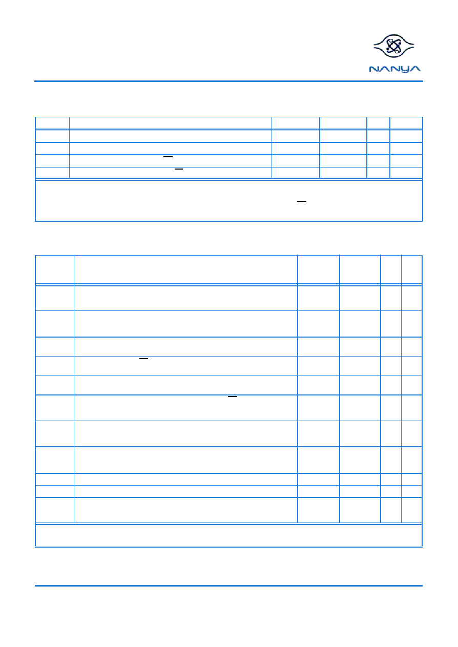
NT5DS64M4AT NT5DS64M4AW
NT5DS32M8AT NT5DS32M8AW
256Mb Double Data Rate SDRAM
REV 1.3
08/2002
57
©
NANYA TECHNOLOGY CORP
. All rights reserved.
NANYA TECHNOLOGY CORP. reserves the right to change Products and Specifications without notice.
AC Input Operating Conditions
(0 ∞C
T
A
70
∞
C
;
V
DDQ
= 2.5V
±
0.2V; V
DD
= 2.5V
±
0.2V, See AC
Characteristics)
Symbol
Parameter/Condition
Min
Max
Unit
Notes
V
IH(AC)
Input High (Logic 1) Voltage, DQ, DQS, and DM Signals
V
REF
+ 0.31
V
1, 2
V
IL(AC)
Input Low (Logic 0) Voltage, DQ, DQS, and DM Signals
V
REF
-
0.31
V
1, 2
V
ID(AC)
Input Differential Voltage, CK and CK Inputs
0.62
V
DDQ
+ 0.6
V
1, 2, 3
V
IX(AC)
Input Crossing Point Voltage, CK and CK Inputs
0.5*V
DDQ
-
0.2 0.5*V
DDQ
+
0.2
V
1, 2, 4
1. Input slew rate = 1V/ns
.
2. Inputs are not recognized as valid until V
REF
stabilizes.
3. V
ID
is the magnitude of the difference between the input level on CK and the input level on CK .
4. The value of V
IX
is expected to equal 0.5*V
DDQ
of the transmitting device and must track variations in the DC level of the same.
I
DD
Specifications and Conditions
(0 ∞C
T
A
70
∞
C
;
V
DDQ
= 2.5V
±
0.2V; V
DD
= 2.5V
±
0.2V, See AC
Characteristics)
Symbol
Parameter/Condition
DDR200
(8B)
t
CK
=10ns
DDR266A/B
(7K/75B)
t
CK
=7.5ns
Unit
Notes
I
D D 0
Operating Current: one bank; active / precharge; t
RC
= t
RC
(min); DQ, DM, and
DQS inputs changing twice per clock cycle; address and control inputs changing
once per clock cycle
75
85
mA
1
I
D D 1
Operating Current: one bank; active / read / precharge; Burst = 2; t
RC
= t
R C
(min); CL = 2.5;
I
OUT
= 0mA; address and control inputs changing once per clock
cycle
110
120
mA
1
I
DD2P
Precharge Power Down Standby Current: all banks idle; Power Down mode;
CKE
V
IL
(max)
25
25
mA
1
I
DD2N
Idle Standby Current: CS
V
IH
(min); all banks idle; CKE
V
IH
(min);
address and control inputs changing once per clock cycle
30
35
mA
1
I
DD3P
Active Power Down Standby Current: one bank active; Power Down mode;
CKE
V
IL
(max)
25
25
mA
1
I
DD3N
Active Standby Current: one bank; active / precharge; CS
V
I H
(min);
CKE
V
I H
(min); t
RC
= t
RAS
(max); DQ, DM, and DQS inputs changing twice per
clock cycle; address and control inputs changing once per clock cycle
50
60
mA
1
I
DD4R
Operating Current: one bank; Burst = 2; reads; continuous burst; address and
control inputs changing once per clock cycle; DQ and DQS outputs changing
twice per clock cycle; CL = 2.5; I
OUT
= 0mA
130
165
mA
1
I
DD4W
Operating Current: one bank; Burst = 2; writes; continuous burst; address and
control inputs changing once per clock cycle; DQ and DQS inputs changing twice
per clock cycle; CL = 2.5
115
150
mA
1
I
D D 5
Auto-Refresh Current : t
RC
= t
RFC
(min)
160
170
mA
1
I
D D 6
Self-Refresh Current : CKE
0.2V
2
2
mA
1, 2
I
D D 7
Operating current: four bank; four bank interleaving with BL = 4, address
and
control inputs randomly changing; 50% of data changing at every transfer;
t
RC
= t
RC
(min); I
OUT
= 0mA.
250
300
mA
1
1. I
DD
specifications are tested after the device is properly initialized.
2. Enables on-chip refresh and address counters.

NT5DS64M4AT NT5DS64M4AW
NT5DS32M8AT NT5DS32M8AW
256Mb Double Data Rate SDRAM
REV 1.3
08/2002
58
©
NANYA TECHNOLOGY CORP
. All rights reserved.
NANYA TECHNOLOGY CORP. reserves the right to change Products and Specifications without notice.
Electrical Characteristics & AC Timing for DDR266/DDR200 - Absolute Specifications
(0
∞
C
T
A
70
∞
C
;
V
DDQ
= 2.5V
±
0.2V; V
DD
= 2.5V
±
0.2V, See AC Characteristics) (Part 1 of 2)
Symbol
Parameter
DDR266A
(-7K)
DDR266B
(-75B)
DDR200
(-8B)
Unit
Notes
Min
Max
Min
Max
Min
Max
t
AC
DQ output access time from CK/CK
-
0.75
+
0.75
-
0.75
+
0.75
-
0.8
+
0.8
ns
1-4
t
DQSCK
DQS output access time from CK/CK
-
0.75
+
0.75
-
0.75
+
0.75
-
0.8
+
0.8
ns
1-4
t
CH
CK high-level width
0.45
0.55
0.45
0.55
0.45
0.55
t
C K
1-4
t
CL
CK low-level width
0.45
0.55
0.45
0.55
0.45
0.55
t
C K
1-4
t
CK
Clock cycle time
CL = 2.5
7
12
7.5
12
8
12
ns
1-4
CL = 2.0
7.5
12
10
12
10
12
ns
1-4
10
12
t
DH
DQ and DM input hold time
0.5
0.5
0.6
ns
1-4, 15,
16
t
DS
DQ and DM input setup time
0.5
0.5
0.6
ns
1-4, 15,
16
t
DIPW
DQ and DM input pulse width (each input)
1.75
1.75
2
ns
1-4
t
HZ
Data-out high-impedance time from CK/CK
-
0.75
+
0.75
-
0.75
+
0.75
-
0.8
+
0.8
ns
1-4, 5
t
LZ
Data-out low-impedance time from CK/CK
-
0.75
+
0.75
-
0.75
+
0.75
-
0.8
+
0.8
ns
1-4, 5
t
DQSQ
DQS-DQ skew (DQS & associated DQ signals)
+
0.5
+
0.5
+
0.6
ns
1-4
t
DQSQA
DQS-DQ skew (DQS & all DQ signals)
+
0.5
+
0.5
+
0.6
ns
1-4
t
HP
minimum half clk period for any given cycle;
defined by clk high (t
CH
) or clk low (t
CL
) time
t
CH
or
t
CL
t
CH
or
t
CL
t
CH
or
t
CL
t
C K
1-4
t
QH
Data output hold time from DQS
t
HP
-
0.75ns
t
HP
-
0.75ns
t
HP
-
1.0ns
t
C K
1-4
t
DQSS
Write command to 1st DQS latching
transition
0.75
1.25
0.75
1.25
0.75
1.25
t
C K
1-4
t
DQSL,H
DQS input low (high) pulse width (write cycle)
0.35
0.35
0.35
t
C K
1-4
t
DSS
DQS falling edge to CK setup time (write cycle)
0.2
0.2
0.2
t
C K
1-4
t
DSH
DQS falling edge hold time from CK (write cycle)
0.2
0.2
0.2
t
C K
1-4
t
MRD
Mode register set command cycle time
14
15
16
ns
1-4
t
WPRES
Write preamble setup time
0
0
0
ns
1-4, 7
t
WPST
Write postamble
0.40
0.60
0.40
0.60
0.40
0.60
t
C K
1-4, 6
t
WPRE
Write preamble
0.25
0.25
0.25
t
C K
1-4
t
IH
Address and control input hold time
(fast slew rate)
0.9
0.9
1.1
ns
2-4, 9,
11, 12
t
IS
Address and control input setup time
(fast slew rate)
0.9
0.9
1.1
ns
2-4, 9,
11, 12
t
IH
Address and control input hold time
(slow slew rate)
1.0
1.0
1.1
ns
2-4, 11,
12, 14
t
IS
Address and control input setup time
(slow slew rate)
1.0
1.0
1.1
ns
2-4, 11,
12, 14
t
IPW
Input pulse width
2.2
2.2
ns
2-4, 12

NT5DS64M4AT NT5DS64M4AW
NT5DS32M8AT NT5DS32M8AW
256Mb Double Data Rate SDRAM
REV 1.3
08/2002
59
©
NANYA TECHNOLOGY CORP
. All rights reserved.
NANYA TECHNOLOGY CORP. reserves the right to change Products and Specifications without notice.
t
RPRE
Read preamble
0.9
1.1
0.9
1.1
0.9
1.1
t
C K
1-4
t
RPST
Read postamble
0.40
0.60
0.40
0.60
0.40
0.60
t
C K
1-4
t
RAS
Active to Precharge command
45
120,000
45
120,000
50
120,000
ns
1-4
t
RC
Active to Active/Auto-refresh command period
65
65
70
ns
1-4
t
RFC
Auto-refresh to Active/Auto-refresh
command period
75
75
80
ns
1-4
t
RCD
Active to Read or Write delay
20
20
20
ns
1-4
t
RAP
Active to Read Command with Autoprecharge
20
20
20
ns
1-4
t
RP
Precharge command period
20
20
20
ns
1-4
t
RRD
Active bank A to Active bank B command
15
15
15
ns
1-4
t
WR
Write recovery time
15
15
15
ns
1-4
t
DAL
Auto precharge write recovery
+ precharge time
(t
WR
/t
CK
)
+
(t
RP
/t
CK
)
(t
WR
/t
CK
)
+
(t
RP
/t
CK
)
(t
WR
/t
CK
)
+
(t
RP
/t
CK
)
t
C K
1-4, 13
t
WTR
Internal write to read command delay
1
1
1
t
C K
1-4
t
XARD
Power down exit time
7.5
7.5
8
ns
1-4
t
XSNR
Exit self-refresh to non-read command
75
75
80
ns
1-4
t
XSRD
Exit self-refresh to read command
200
200
200
t
C K
1-4
t
REFI
Average Periodic Refresh Interval
7.8
7.8
7.8
µ
s
1-4, 8
Electrical Characteristics & AC Timing for DDR266/DDR200 - Absolute Specifications
(0
∞
C
T
A
70
∞
C
;
V
DDQ
= 2.5V
±
0.2V; V
DD
= 2.5V
±
0.2V, See AC Characteristics) (Part 2 of 2)
Symbol
Parameter
DDR266A
(-7K)
DDR266B
(-75B)
DDR200
(-8B)
Unit
Notes
Min
Max
Min
Max
Min
Max

NT5DS64M4AT NT5DS64M4AW
NT5DS32M8AT NT5DS32M8AW
256Mb Double Data Rate SDRAM
REV 1.3
08/2002
60
©
NANYA TECHNOLOGY CORP
. All rights reserved.
NANYA TECHNOLOGY CORP. reserves the right to change Products and Specifications without notice.
Electrical Characteristics & AC Timing for DDR266 - Applicable Specifications
Expressed in Clock Cycles
(0
∞
C
T
A
70
∞
C
;
V
DDQ
= 2.5V
±
0.2V; V
DD
= 2.5V
±
0.2V, See AC Characteristics)
Symbol
Parameter
t
CK
= 7.5ns
Units
Notes
Min
Max
t
MRD
Mode register set command cycle time
2
t
CK
1-4
t
WPRE
Write preamble
0.25
t
CK
1-4
t
RAS
Active to Precharge command
6
16000
t
CK
1-4
t
RC
Active to Active/Auto-refresh command period
9
t
CK
1-4
t
RFC
Auto-refresh to Active/Auto-refresh
command period
10
t
CK
1-4
t
RCD
Active to Read or Write delay
3
t
CK
1-4
t
RAP
Active to Read Command with Autoprecharge
3
t
CK
1-4
t
RP
Precharge command period
3
t
CK
1-4
t
RRD
Active bank A to Active bank B command
2
t
CK
1-4
t
WR
Write recovery time
2
t
CK
1-4
t
DAL
Auto precharge write recovery + precharge time
5
t
CK
1-5
t
WTR
Internal write to read command delay
1
t
CK
1-4
t
XSNR
Exit self-refresh to non-read command
10
t
CK
1-4
t
XSRD
Exit self-refresh to read command
200
t
CK
1-4
1. Input slew rate = 1V/ns
2. The CK/CK input reference level (for timing reference to CK/CK) is the point at which CK and CK cross: the input reference level for sig-
nals other than CK/CK , is V
REF.
3. Inputs are not recognized as valid until V
REF
stabilizes.
4. The Output timing reference level, as measured at the timing reference point indicated in AC Characteristics (Note 3) is V
TT
.
5. t
H Z
and t
LZ
transitions occur in the same access time windows as valid data transitions. These parameters are not referred to a specific
voltage level, but specify when the device is no longer driving (HZ), or begins driving (LZ).

NT5DS64M4AT NT5DS64M4AW
NT5DS32M8AT NT5DS32M8AW
256Mb Double Data Rate SDRAM
REV 1.3
08/2002
61
©
NANYA TECHNOLOGY CORP
. All rights reserved.
NANYA TECHNOLOGY CORP. reserves the right to change Products and Specifications without notice.
Electrical Characteristics & AC Timing for DDR266/DDR200 - Absolute Specifications
Notes
1. Input slew rate = 1V/ns.
2. The CK/CK input reference level (for timing reference to CK/CK) is the point at which CK and CK cross:
the input reference level for signals other than CK/CK, is V
REF.
3. Inputs are not recognized as valid until V
REF
stabilizes.
4. The Output timing reference level, as measured at the timing reference point indicated in AC Characteristics (Note 3) is V
TT
.
5. t
HZ
and t
LZ
transitions occur in the same access time windows as valid data transitions. These parameters are not referred
to a specific voltage level, but specify when the device is no longer driving (HZ), or begins driving (LZ).
6. The maximum limit for this parameter is not a device limit. The device operates with a greater value for this parameter, but
system performance (bus turnaround) degrades accordingly.
7. The specific requirement is that DQS be valid (high, low, or some point on a valid transition) on or before this CK edge. A
valid
transition is defined as monotonic and meeting the input slew rate specifications of the device. When no writes were prev-
iously in progress on the bus, DQS will be transitioning from Hi-Z to logic LOW. If a previous write was in progress, DQS
could be HIGH, LOW, or transitioning from high to low at this time, depending on t
DQSS
.
8. A maximum of eight Autorefresh commands can be posted to any given DDR SDRAM device.
9. For command/address input slew rate
1.0V/ns. Slew rate is measured between V
OH
(AC) and V
OL
(AC).
10. For command/address input slew rate
0.5V/ns and < 1.0V/ns. Slew rate is measured between V
OH
(AC) and V
O L
(AC)
11. CK/CK slew rates are
1.0V/ns.
12.These parameters guarantee device timing, but they are not necessarily tested on each device, and they may be guara-
nteed by design or tester characterization.
13. For each of the terms in parentheses, if not already an integer, round to the next highest integer. t
CK
is equal to the actual
system clock cycle time.
For example, for DDR266B at CL = 2.5, t
DAL
= (15ns/7.5ns) +(20ns/7.5ns) = 2 + 3 = 5.

NT5DS64M4AT NT5DS64M4AW
NT5DS32M8AT NT5DS32M8AW
256Mb Double Data Rate SDRAM
REV 1.3
08/2002
62
©
NANYA TECHNOLOGY CORP
. All rights reserved.
NANYA TECHNOLOGY CORP. reserves the right to change Products and Specifications without notice.
14. An input setup and hold time derating table is used to increase t
IS
and t
IH
in the case where the input slew
rate is below 0.5 V/ns.
15. An input setup and hold time derating table is used to increase t
DS
and t
DH
in the case where the I/O slew rate is below
0.5 V/ns.
16. An I/O Delta Rise, Fall Derating table is used to increase t
DS
and t
DH)
in the case where DQ, DM, and DQS slew rates
differ.
Input Slew Rate
delta
( t
IS)
delta
( t
IH)
Unit
Notes
0.5 V/ns
0
0
ps
1,2
0.4 V/ns
+50
0
ps
1,2
0.3 V/ns
+100
0
ps
1,2
1. Input slew rate is based on the lesser of the slew rates determined by either V
IH (AC)
to V
IL (AC)
or V
IH (DC)
to V
IL (DC)
, similarly for rising
transitions.
2. These derating parameters may be guaranteed by design or tester characterization and are not necessarily tested on eachdevice.
Input Slew Rate
delta
( t
DS)
delta
( t
DH)
Unit
Notes
0.5 V/ns
0
0
ps
1,2
0.4 V/ns
+75
+75
ps
1,2
0.3 V/ns
+150
+150
ps
1,2
1. I/O slew rate is based on the lesser of the slew rates determined by either V
IH (AC)
to V
IL (AC)
or V
IH (DC)
to V
IL (DC)
, similarly for rising
transitions.
2. These derating parameters may be guaranteed by design or tester characterization and are not necessarily tested on eachdevice.
Input Slew Rate
delta
( t
DS)
delta
( t
DH)
Unit
Notes
0.0 V/ns
0
0
ps
1,2,3,4
0.25 V/ns
+50
+50
ps
1,2,3,4
0.5 V/ns
+100
+100
ps
1,2,3,4
1. Input slew rate is based on the lesser of the slew rates determined by either V
IH (AC)
to V
IL (AC)
or V
IH (DC)
to V
IL (DC)
, similarly for rising
transitions.
2. Input slew rate is based on the larger of AC to AC delta rise, fall rate and DC to DC delta rise, fall rate.
3. The delta rise, fall rate is calculated as: [1/(slew rate 1)] - [1/(slew rate 2)]
For example: slew rate 1 = 0.5 V/ns; slew rate 2 = 0.4 V/ns
Delta rise, fall = (1/0.5) - (1/0.4) [ns/V]
= -0.5 ns/V
Using the table above, this would result in an increase in t
DS
and t
DH
of 100 ps.
4. These derating parameters may be guaranteed by design or tester characterization and are not necessarily tested on each device.

NT5DS64M4AT NT5DS64M4AW
NT5DS32M8AT NT5DS32M8AW
256Mb Double Data Rate SDRAM
REV 1.3
08/2002
63
©
NANYA TECHNOLOGY CORP
. All rights reserved.
NANYA TECHNOLOGY CORP. reserves the right to change Products and Specifications without notice.
Data Input (Write)
(Timing Burst Length = 4)
Data Output (Read)
(Timing Burst Length = 4)
t
DH
t
DS
t
DH
t
DS
t
DSL
DI n = Data In for column n.
3 subsequent elements of data in are applied in programmed order following DI n.
DI n
DQS
DQ
DM
Don't Care
t
DSH
t
DQSQ
(max)occurs when DQS is the earliest among DQS and DQ signals to transition.
DQS
DQ
t
DQSQ
t
DQSQ
Data Output hold time from Data Strobe is shown as t
QH
. t
Q H
is a function of the clock high or low time (t
HP
)
t
QH2
t
QH1
t
DQSQ
t
QH3
t
QH4
t
DQSQ
CK
CK
t
HP
t
HP
t
HP
t
HP1
t
HP2
t
HP3
t
HP4
t
HP
is the half cycle pulse width for each half cycle clock. t
HP
is referenced to the clock duty cycle only
and not to the data strobe (DQS) duty cycle.
for that given clock cycle. Note correlation of t
H P
to t
Q H
in the diagram above (t
HP1
to t
QH1
, etc.).

NT5DS64M4AT NT5DS64M4AW
NT5DS32M8AT NT5DS32M8AW
256Mb Double Data Rate SDRAM
REV 1.3
08/2002
64
©
NANYA TECHNOLOGY CORP
. All rights reserved.
NANYA TECHNOLOGY CORP. reserves the right to change Products and Specifications without notice.
Initialize and Mode Register Sets
t
I
H
2
0
0
µ
s
t
I
S
t
I
H
t
I
S
t
I
H
t
I
S
t
I
H
t
I
S
t
I
H
t
I
S
t
I
H
t
I
S
t
I
H
t
I
S
t
M
R
D
t
R
F
C
t
R
F
C
t
R
P
t
M
R
D
t
M
R
D
t
C
L
t
C
K
t
C
H
t
V
T
D
P
R
E
E
M
R
S
M
R
S
P
R
E
A
R
A
R
M
R
S
N
O
P
A
C
T
C
O
D
E
C
O
D
E
C
O
D
E
R
A
C
O
D
E
C
O
D
E
C
O
D
E
R
A
B
A
0
=
L
B
A
0
=
L
B
A
H
i
g
h
-
Z
H
i
g
h
-
Z
P
o
w
e
r
-
u
p
:
V
D
D
a
n
d
C
K
s
t
a
b
l
e
E
x
t
e
n
d
e
d
M
o
d
e
R
e
g
i
s
t
e
r
S
e
t
L
o
a
d
M
o
d
e
R
e
g
i
s
t
e
r
,
R
e
s
e
t
D
L
L
L
o
a
d
M
o
d
e
R
e
g
i
s
t
e
r
(
w
i
t
h
A
8
=
L
)
V
D
D
V
D
D
Q
V
T
T
(
S
y
s
t
e
m
*
)
V
R
E
F
C
K
C
K
E
C
o
m
m
a
n
d
D
M
A
0
-
A
9
,
A
1
1
A
1
0
B
A
0
,
B
A
1
D
Q
S
D
Q
L
V
C
M
O
S
L
O
W
L
E
V
E
L
A
L
L
B
A
N
K
S
B
A
0
=
H
B
A
1
=
L
B
A
1
=
L
B
A
1
=
L
A
L
L
B
A
N
K
S
*
V
T
T
i
s
n
o
t
a
p
p
l
i
e
d
d
i
r
e
c
t
l
y
t
o
t
h
e
d
e
v
i
c
e
,
h
o
w
e
v
e
r
t
V
T
D
m
u
s
t
b
e
*
*
t
M
R
D
i
s
r
e
q
u
i
r
e
d
b
e
f
o
r
e
a
n
y
c
o
m
m
a
n
d
c
a
n
b
e
a
p
p
l
i
e
d
a
n
d
T
h
e
t
w
o
A
u
t
o
r
e
f
r
e
s
h
c
o
m
m
a
n
d
s
m
a
y
b
e
m
o
v
e
d
t
o
f
o
l
l
o
w
t
h
e
f
i
r
s
t
M
R
S
,
g
r
e
a
t
e
r
t
h
a
n
o
r
e
q
u
a
l
t
o
z
e
r
o
t
o
a
v
o
i
d
d
e
v
i
c
e
l
a
t
c
h
u
p
.
2
0
0
c
y
c
l
e
s
o
f
C
K
a
r
e
r
e
q
u
i
r
e
d
b
e
f
o
r
e
a
R
e
a
d
c
o
m
m
a
n
d
c
a
n
b
e
a
p
p
l
i
e
d
.
b
u
t
p
r
e
c
e
d
e
t
h
e
s
e
c
o
n
d
P
r
e
c
h
a
r
g
e
A
l
l
c
o
m
m
a
n
d
.
D
o
n
'
t
C
a
r
e
2
0
0
c
y
c
l
e
s
o
f
C
K
*
*
C
K

NT5DS64M4AT NT5DS64M4AW
NT5DS32M8AT NT5DS32M8AW
256Mb Double Data Rate SDRAM
REV 1.3
08/2002
65
©
NANYA TECHNOLOGY CORP
. All rights reserved.
NANYA TECHNOLOGY CORP. reserves the right to change Products and Specifications without notice.
Power Down Mode
t
I
H
t
I
S
t
I
H
t
I
S
t
I
S
t
I
S
t
I
H
t
I
S
t
C
L
t
C
H
t
C
K
N
O
P
V
A
L
I
D
V
A
L
I
D
*
V
A
L
I
D
V
A
L
I
D
E
n
t
e
r
P
o
w
e
r
D
o
w
n
M
o
d
e
E
x
i
t
P
o
w
e
r
D
o
w
n
M
o
d
e
N
o
c
o
l
u
m
n
a
c
c
e
s
s
e
s
a
r
e
a
l
l
o
w
e
d
t
o
b
e
i
n
p
r
o
g
r
e
s
s
a
t
t
h
e
t
i
m
e
p
o
w
e
r
d
o
w
n
i
s
e
n
t
e
r
e
d
.
*
=
I
f
t
h
i
s
c
o
m
m
a
n
d
i
s
a
P
r
e
c
h
a
r
g
e
(
o
r
i
f
t
h
e
d
e
v
i
c
e
i
s
a
l
r
e
a
d
y
i
n
t
h
e
i
d
l
e
s
t
a
t
e
)
t
h
e
n
t
h
e
p
o
w
e
r
d
o
w
n
m
o
d
e
s
h
o
w
n
i
s
P
r
e
c
h
a
r
g
e
p
o
w
e
r
d
o
w
n
.
I
f
t
h
i
s
c
o
m
m
a
n
d
i
s
a
n
A
c
t
i
v
e
(
o
r
i
f
a
t
l
e
a
s
t
o
n
e
r
o
w
i
s
a
l
r
e
a
d
y
a
c
t
i
v
e
)
,
t
h
e
n
t
h
e
p
o
w
e
r
d
o
w
n
m
o
d
e
s
h
o
w
n
i
s
A
c
t
i
v
e
p
o
w
e
r
d
o
w
n
.
C
K
E
C
o
m
m
a
n
d
A
D
D
R
D
Q
S
D
Q
D
M
D
o
n
'
t
C
a
r
e
C
K
C
K
N
O
P
t
X
A
R
D
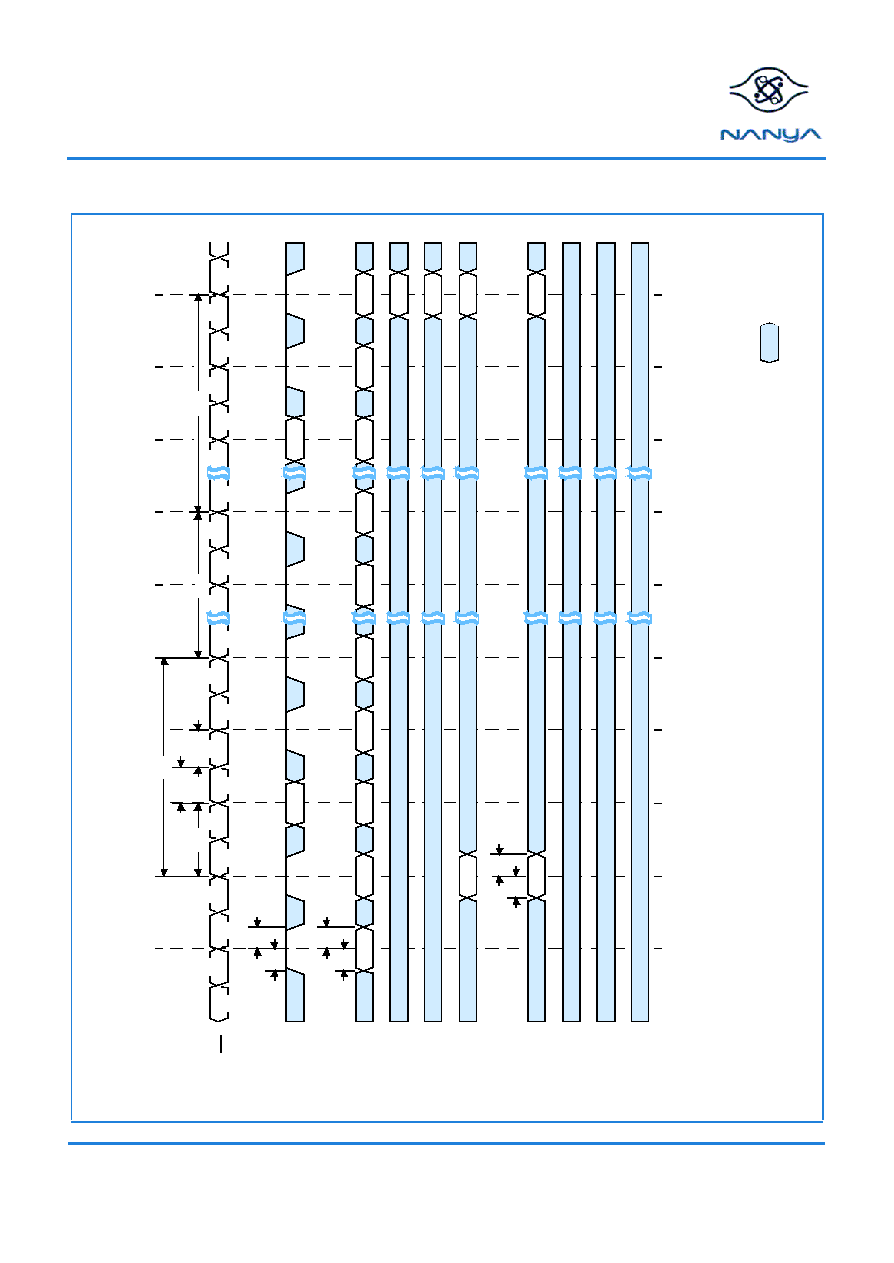
NT5DS64M4AT NT5DS64M4AW
NT5DS32M8AT NT5DS32M8AW
256Mb Double Data Rate SDRAM
REV 1.3
08/2002
66
©
NANYA TECHNOLOGY CORP
. All rights reserved.
NANYA TECHNOLOGY CORP. reserves the right to change Products and Specifications without notice.
Auto Refresh Mode
t
I
H
t
I
S
t
I
H
t
I
S
t
I
H
t
I
S
t
R
F
C
t
R
P
t
C
L
t
C
H
t
C
K
P
R
E
N
O
P
N
O
P
A
R
N
O
P
A
R
N
O
P
N
O
P
N
O
P
R
A
R
A
B
A
P
R
E
=
P
r
e
c
h
a
r
g
e
;
A
C
T
=
A
c
t
i
v
e
;
R
A
=
R
o
w
a
d
d
r
e
s
s
;
B
A
=
B
a
n
k
a
d
d
r
e
s
s
;
A
R
=
A
u
t
o
r
e
f
r
e
s
h
.
N
O
P
c
o
m
m
a
n
d
s
a
r
e
s
h
o
w
n
f
o
r
e
a
s
e
o
f
i
l
l
u
s
t
r
a
t
i
o
n
;
o
t
h
e
r
v
a
l
i
d
c
o
m
m
a
n
d
s
m
a
y
b
e
p
o
s
s
i
b
l
e
a
t
t
h
e
s
e
t
i
m
e
s
.
D
M
,
D
Q
,
a
n
d
D
Q
S
s
i
g
n
a
l
s
a
r
e
a
l
l
d
o
n
'
t
c
a
r
e
/
h
i
g
h
-
Z
f
o
r
o
p
e
r
a
t
i
o
n
s
s
h
o
w
n
.
V
A
L
I
D
V
A
L
I
D
A
C
T
R
A
C
K
E
C
o
m
m
a
n
d
A
0
-
A
8
A
9
,
A
1
1
,
A
1
2
A
1
0
B
A
0
,
B
A
1
D
Q
S
D
Q
D
M
B
A
N
K
(
S
)
D
o
n
'
t
C
a
r
e
A
L
L
B
A
N
K
S
O
N
E
B
A
N
K
t
R
F
C
C
K
C
K

NT5DS64M4AT NT5DS64M4AW
NT5DS32M8AT NT5DS32M8AW
256Mb Double Data Rate SDRAM
REV 1.3
08/2002
67
©
NANYA TECHNOLOGY CORP
. All rights reserved.
NANYA TECHNOLOGY CORP. reserves the right to change Products and Specifications without notice.
Self Refresh Mode
2
0
0
c
y
c
l
e
s
t
I
H
t
I
S
t
X
S
R
D
,
t
X
S
R
N
t
I
H
t
I
S
t
I
S
t
I
S
t
I
H
t
I
S
t
R
P
*
t
C
K
t
C
L
t
C
H
A
R
V
A
L
I
D
N
O
P
V
A
L
I
D
E
n
t
e
r
S
e
l
f
R
e
f
r
e
s
h
M
o
d
e
E
x
i
t
S
e
l
f
R
e
f
r
e
s
h
M
o
d
e
N
O
P
*
=
D
e
v
i
c
e
m
u
s
t
b
e
i
n
t
h
e
a
l
l
b
a
n
k
s
i
d
l
e
s
t
a
t
e
b
e
f
o
r
e
e
n
t
e
r
i
n
g
S
e
l
f
R
e
f
r
e
s
h
M
o
d
e
.
*
*
=
t
X
S
N
R
i
s
r
e
q
u
i
r
e
d
b
e
f
o
r
e
a
n
y
n
o
n
-
r
e
a
d
c
o
m
m
a
n
d
c
a
n
b
e
a
p
p
l
i
e
d
,
a
n
d
t
X
S
R
D
(
2
0
0
c
y
c
l
e
s
o
f
C
K
)
.
C
K
E
C
o
m
m
a
n
d
A
D
D
R
D
Q
S
D
Q
D
M
D
o
n
'
t
C
a
r
e
a
r
e
r
e
q
u
i
r
e
d
b
e
f
o
r
e
a
R
e
a
d
c
o
m
m
a
n
d
c
a
n
b
e
a
p
p
l
i
e
d
.
C
K
C
K
C
l
o
c
k
m
u
s
t
b
e
s
t
a
b
l
e
b
e
f
o
r
e
e
x
i
t
i
n
g
S
e
l
f
R
e
f
r
e
s
h
M
o
d
e

NT5DS64M4AT NT5DS64M4AW
NT5DS32M8AT NT5DS32M8AW
256Mb Double Data Rate SDRAM
REV 1.3
08/2002
68
©
NANYA TECHNOLOGY CORP
. All rights reserved.
NANYA TECHNOLOGY CORP. reserves the right to change Products and Specifications without notice.
Read without Auto Precharge (Burst Length = 4)
t
H
Z
(
m
a
x
)
t
L
Z
(
m
a
x
)
t
H
Z
(
m
i
n
)
t
R
P
S
T
t
L
Z
(
m
i
n
)
t
I
H
t
I
S
t
I
H
t
I
S
t
I
H
t
I
S
t
I
H
t
I
S
t
I
H
t
I
H
t
I
S
t
R
P
t
C
L
t
C
H
t
C
K
P
R
E
N
O
P
N
O
P
A
C
T
N
O
P
N
O
P
N
O
P
N
O
P
D
O
n
=
d
a
t
a
o
u
t
f
r
o
m
c
o
l
u
m
n
n
.
3
s
u
b
s
e
q
u
e
n
t
e
l
e
m
e
n
t
s
o
f
d
a
t
a
o
u
t
a
r
e
p
r
o
v
i
d
e
d
i
n
t
h
e
p
r
o
g
r
a
m
m
e
d
o
r
d
e
r
f
o
l
l
o
w
i
n
g
D
O
n
.
*
=
D
o
n
'
t
c
a
r
e
i
f
A
1
0
i
s
H
i
g
h
a
t
t
h
i
s
p
o
i
n
t
.
P
R
E
=
P
r
e
c
h
a
r
g
e
;
A
C
T
=
A
c
t
i
v
e
;
R
A
=
R
o
w
a
d
d
r
e
s
s
;
B
A
=
B
a
n
k
a
d
d
r
e
s
s
.
N
O
P
c
o
m
m
a
n
d
s
a
r
e
s
h
o
w
n
f
o
r
e
a
s
e
o
f
i
l
l
u
s
t
r
a
t
i
o
n
;
o
t
h
e
r
c
o
m
m
a
n
d
s
m
a
y
b
e
v
a
l
i
d
a
t
t
h
e
s
e
t
i
m
e
s
.
B
A
x
B
A
x
V
A
L
I
D
V
A
L
I
D
V
A
L
I
D
N
O
P
R
e
a
d
C
O
L
n
R
A
R
A
B
A
x
*
D
O
n
C
K
E
C
o
m
m
a
n
d
A
1
0
B
A
0
,
B
A
1
D
M
D
Q
S
D
Q
D
Q
S
D
Q
A
0
-
A
9
,
A
1
1
,
A
1
2
A
L
L
B
A
N
K
S
O
N
E
B
A
N
K
t
D
Q
S
C
K
(
m
a
x
)
t
R
P
R
E
C
L
=
2
t
R
P
R
E
D
o
n
'
t
C
a
r
e
C
a
s
e
1
:
t
A
C
/
t
D
Q
S
C
K
=
m
i
n
C
a
s
e
2
:
t
A
C
/
t
D
Q
S
C
K
=
m
a
x
t
R
P
S
T
t
A
C
(
m
a
x
)
t
L
Z
(
m
a
x
)
t
D
Q
S
C
K
(
m
i
n
)
t
A
C
(
m
i
n
)
D
O
n
C
K
C
K
D
I
S
A
P
D
I
S
A
P
=
D
i
s
a
b
l
e
A
u
t
o
P
r
e
c
h
a
r
g
e
.

NT5DS64M4AT NT5DS64M4AW
NT5DS32M8AT NT5DS32M8AW
256Mb Double Data Rate SDRAM
REV 1.3
08/2002
69
©
NANYA TECHNOLOGY CORP
. All rights reserved.
NANYA TECHNOLOGY CORP. reserves the right to change Products and Specifications without notice.
Read with Auto Precharge (Burst Length = 4)
t
H
Z
(
m
a
x
)
t
L
Z
(
m
a
x
)
t
H
Z
(
m
i
n
)
t
R
P
S
T
t
L
Z
(
m
i
n
)
t
I
H
t
I
S
t
I
H
t
I
S
t
I
H
t
I
S
t
I
H
t
I
S
t
I
H
t
I
H
t
I
S
t
R
P
t
C
L
t
C
H
t
C
K
N
O
P
N
O
P
N
O
P
A
C
T
N
O
P
N
O
P
N
O
P
N
O
P
D
O
n
=
d
a
t
a
o
u
t
f
r
o
m
c
o
l
u
m
n
n
.
3
s
u
b
s
e
q
u
e
n
t
e
l
e
m
e
n
t
s
o
f
d
a
t
a
o
u
t
a
r
e
p
r
o
v
i
d
e
d
i
n
t
h
e
p
r
o
g
r
a
m
m
e
d
o
r
d
e
r
f
o
l
l
o
w
i
n
g
D
O
n
.
E
N
A
P
=
e
n
a
b
l
e
A
u
t
o
P
r
e
c
h
a
r
g
e
.
A
C
T
=
a
c
t
i
v
e
;
R
A
=
r
o
w
a
d
d
r
e
s
s
.
N
O
P
c
o
m
m
a
n
d
s
a
r
e
s
h
o
w
n
f
o
r
e
a
s
e
o
f
i
l
l
u
s
t
r
a
t
i
o
n
;
o
t
h
e
r
c
o
m
m
a
n
d
s
m
a
y
b
e
v
a
l
i
d
a
t
t
h
e
s
e
t
i
m
e
s
.
B
A
x
V
A
L
I
D
V
A
L
I
D
V
A
L
I
D
N
O
P
R
e
a
d
C
O
L
n
R
A
R
A
D
O
n
C
K
E
C
o
m
m
a
n
d
A
1
0
B
A
0
,
B
A
1
D
M
D
Q
S
D
Q
D
Q
S
D
Q
A
0
-
A
9
,
A
1
1
,
A
1
2
t
D
Q
S
C
K
(
m
a
x
)
t
R
P
R
E
C
L
=
2
t
R
P
R
E
D
o
n
'
t
C
a
r
e
C
a
s
e
1
:
t
A
C
/
t
D
Q
S
C
K
=
m
i
n
C
a
s
e
2
:
t
A
C
/
t
D
Q
S
C
K
=
m
a
x
t
R
P
S
T
t
A
C
(
m
a
x
)
t
L
Z
(
m
a
x
)
t
D
Q
S
C
K
(
m
i
n
)
t
A
C
(
m
i
n
)
D
O
n
E
N
A
P
B
A
x
C
K
C
K
t
H
Z
(
m
i
n
)

NT5DS64M4AT NT5DS64M4AW
NT5DS32M8AT NT5DS32M8AW
256Mb Double Data Rate SDRAM
REV 1.3
08/2002
70
©
NANYA TECHNOLOGY CORP
. All rights reserved.
NANYA TECHNOLOGY CORP. reserves the right to change Products and Specifications without notice.
Bank Read Access (Burst Length = 4)
t
H
Z
(
m
a
x
)
t
L
Z
(
m
a
x
)
t
H
Z
(
m
i
n
)
t
R
P
S
T
t
L
Z
(
m
i
n
)
t
I
H
t
I
S
t
I
H
t
I
S
t
I
H
t
I
S
t
I
H
t
I
S
t
I
H
t
I
S
t
C
L
t
C
H
t
C
K
R
e
a
d
N
O
P
P
R
E
N
O
P
N
O
P
A
C
T
N
O
P
N
O
P
B
A
x
B
A
x
*
V
A
L
I
D
N
O
P
A
C
T
R
A
R
A
B
A
x
D
O
n
C
K
C
K
C
K
E
C
o
m
m
a
n
d
A
1
0
B
A
0
,
B
A
1
D
M
D
Q
S
D
Q
D
Q
S
D
Q
t
D
Q
S
C
K
(
m
a
x
)
t
R
P
R
E
C
L
=
2
C
L
=
2
t
R
P
R
E
D
o
n
'
t
C
a
r
e
C
a
s
e
1
:
t
A
C
/
t
D
Q
S
C
K
=
m
i
n
C
a
s
e
2
:
t
A
C
/
t
D
Q
S
C
K
=
m
a
x
t
R
P
S
T
t
A
C
(
m
a
x
)
t
L
Z
(
m
a
x
)
t
D
Q
S
C
K
(
m
i
n
)
t
A
C
(
m
i
n
)
D
O
n
C
O
L
n
R
A
R
A
A
L
L
B
A
N
K
S
R
A
O
N
E
B
A
N
K
D
I
S
A
P
B
A
x
t
R
P
D
O
n
=
d
a
t
a
o
u
t
f
r
o
m
c
o
l
u
m
n
n
.
3
s
u
b
s
e
q
u
e
n
t
e
l
e
m
e
n
t
s
o
f
d
a
t
a
o
u
t
a
r
e
p
r
o
v
i
d
e
d
i
n
t
h
e
p
r
o
g
r
a
m
m
e
d
o
r
d
e
r
f
o
l
l
o
w
i
n
g
D
O
n
.
D
I
S
A
P
=
d
i
s
a
b
l
e
A
u
t
o
P
r
e
c
h
a
r
g
e
.
*
=
D
o
n
'
t
c
a
r
e
i
f
A
1
0
i
s
H
i
g
h
a
t
t
h
i
s
p
o
i
n
t
.
P
R
E
=
P
r
e
c
h
a
r
g
e
;
A
C
T
=
A
c
t
i
v
e
;
R
A
=
R
o
w
a
d
d
r
e
s
s
;
B
A
=
B
a
n
k
a
d
d
r
e
s
s
.
N
O
P
c
o
m
m
a
n
d
s
a
r
e
s
h
o
w
n
f
o
r
e
a
s
e
o
f
i
l
l
u
s
t
r
a
t
i
o
n
;
o
t
h
e
r
c
o
m
m
a
n
d
s
m
a
y
b
e
v
a
l
i
d
a
t
t
h
e
s
e
t
i
m
e
s
.
t
R
C
D
A
0
-
A
9
,
A
1
1
,
A
1
2
t
R
A
S
t
R
C
t
L
Z
(
m
i
n
)

NT5DS64M4AT NT5DS64M4AW
NT5DS32M8AT NT5DS32M8AW
256Mb Double Data Rate SDRAM
REV 1.3
08/2002
71
©
NANYA TECHNOLOGY CORP
. All rights reserved.
NANYA TECHNOLOGY CORP. reserves the right to change Products and Specifications without notice.
Write without Auto Precharge (Burst Length = 4)
t
I
H
t
W
P
S
T
t
D
Q
S
L
t
I
H
t
I
S
t
I
H
t
I
S
t
I
H
t
I
S
t
I
H
t
I
S
t
I
H
t
I
S
t
R
P
t
C
L
t
C
H
t
C
K
N
O
P
N
O
P
N
O
P
P
R
E
N
O
P
N
O
P
A
C
T
N
O
P
B
A
x
B
A
N
O
P
W
r
i
t
e
C
O
L
n
R
A
R
A
B
A
x
*
V
A
L
I
D
D
I
n
=
D
a
t
a
i
n
f
o
r
c
o
l
u
m
n
n
.
3
s
u
b
s
e
q
u
e
n
t
e
l
e
m
e
n
t
s
o
f
d
a
t
a
i
n
a
r
e
a
p
p
l
i
e
d
i
n
t
h
e
p
r
o
g
r
a
m
m
e
d
o
r
d
e
r
f
o
l
l
o
w
i
n
g
D
I
n
.
D
I
S
A
P
=
D
i
s
a
b
l
e
A
u
t
o
P
r
e
c
h
a
r
g
e
.
*
=
D
o
n
'
t
c
a
r
e
i
f
A
1
0
i
s
H
i
g
h
a
t
t
h
i
s
p
o
i
n
t
.
P
R
E
=
P
r
e
c
h
a
r
g
e
;
A
C
T
=
A
c
t
i
v
e
;
R
A
=
R
o
w
a
d
d
r
e
s
s
;
B
A
=
B
a
n
k
a
d
d
r
e
s
s
.
N
O
P
c
o
m
m
a
n
d
s
a
r
e
s
h
o
w
n
f
o
r
e
a
s
e
o
f
i
l
l
u
s
t
r
a
t
i
o
n
;
o
t
h
e
r
v
a
l
i
d
c
o
m
m
a
n
d
s
m
a
y
b
e
p
o
s
s
i
b
l
e
a
t
t
h
e
s
e
t
i
m
e
s
.
D
I
n
C
K
C
K
C
K
E
C
o
m
m
a
n
d
A
1
0
B
A
0
,
B
A
1
D
Q
S
D
Q
D
M
D
I
S
A
P
A
L
L
B
A
N
K
S
O
N
E
B
A
N
K
t
W
R
t
W
P
R
E
S
t
D
Q
S
H
D
o
n
'
t
C
a
r
e
A
0
-
A
9
,
A
1
1
,
A
1
2
t
D
Q
S
S
=
m
i
n
.
t
D
Q
S
S
t
W
P
R
E
t
D
S
H

NT5DS64M4AT NT5DS64M4AW
NT5DS32M8AT NT5DS32M8AW
256Mb Double Data Rate SDRAM
REV 1.3
08/2002
72
©
NANYA TECHNOLOGY CORP
. All rights reserved.
NANYA TECHNOLOGY CORP. reserves the right to change Products and Specifications without notice.
Write with Auto Precharge (Burst Length = 4)
N
O
P
c
o
m
m
a
n
d
s
a
r
e
s
h
o
w
n
f
o
r
e
a
s
e
o
f
i
l
l
u
s
t
r
a
t
i
o
n
;
o
t
h
e
r
v
a
l
i
d
c
o
m
m
a
n
d
s
m
a
y
b
e
p
o
s
s
i
b
l
e
a
t
t
h
e
s
e
t
i
m
e
s
.
A
C
T
=
A
c
t
i
v
e
;
R
A
=
R
o
w
a
d
d
r
e
s
s
;
B
A
=
B
a
n
k
a
d
d
r
e
s
s
.
t
I
H
t
W
P
S
T
t
D
Q
S
L
t
I
H
t
I
S
t
I
H
t
I
S
t
I
H
t
I
S
t
I
H
t
I
S
t
I
S
t
R
P
t
C
L
t
C
H
t
C
K
N
O
P
N
O
P
N
O
P
N
O
P
N
O
P
N
O
P
A
C
T
N
O
P
B
A
x
B
A
N
O
P
W
r
i
t
e
C
O
L
n
R
A
R
A
V
A
L
I
D
D
I
n
=
D
a
t
a
i
n
f
o
r
c
o
l
u
m
n
n
.
3
s
u
b
s
e
q
u
e
n
t
e
l
e
m
e
n
t
s
o
f
d
a
t
a
i
n
a
r
e
a
p
p
l
i
e
d
i
n
t
h
e
p
r
o
g
r
a
m
m
e
d
o
r
d
e
r
f
o
l
l
o
w
i
n
g
D
I
n
.
E
N
A
P
=
E
n
a
b
l
e
A
u
t
o
P
r
e
c
h
a
r
g
e
.
C
K
C
K
C
K
E
C
o
m
m
a
n
d
A
1
0
B
A
0
,
B
A
1
D
Q
S
D
Q
D
M
t
W
R
t
D
Q
S
S
t
W
P
R
E
S
t
D
Q
S
H
D
o
n
'
t
C
a
r
e
V
A
L
I
D
V
A
L
I
D
E
N
A
P
A
0
-
A
9
,
A
1
1
,
A
1
2
t
D
A
L
t
D
Q
S
S
=
m
i
n
.
t
D
S
H
t
W
P
R
E
D
I
n

NT5DS64M4AT NT5DS64M4AW
NT5DS32M8AT NT5DS32M8AW
256Mb Double Data Rate SDRAM
REV 1.3
08/2002
73
©
NANYA TECHNOLOGY CORP
. All rights reserved.
NANYA TECHNOLOGY CORP. reserves the right to change Products and Specifications without notice.
Bank Write Access (Burst Length = 4)
t
W
P
S
T
t
D
Q
S
L
t
I
H
t
I
S
t
I
H
t
I
S
t
I
H
t
I
S
t
I
H
t
I
S
t
I
H
t
I
S
t
C
L
t
C
H
t
C
K
t
R
A
S
W
r
i
t
e
N
O
P
N
O
P
N
O
P
N
O
P
P
R
E
N
O
P
N
O
P
B
A
x
N
O
P
A
C
T
R
A
R
A
D
I
n
=
d
a
t
a
i
n
f
o
r
c
o
l
u
m
n
n
.
3
s
u
b
s
e
q
u
e
n
t
e
l
e
m
e
n
t
s
o
f
d
a
t
a
i
n
a
r
e
a
p
p
l
i
e
d
i
n
t
h
e
p
r
o
g
r
a
m
m
e
d
o
r
d
e
r
f
o
l
l
o
w
i
n
g
D
I
n
.
D
I
S
A
P
=
D
i
s
a
b
l
e
A
u
t
o
P
r
e
c
h
a
r
g
e
.
*
=
d
o
n
'
t
c
a
r
e
i
f
A
1
0
i
s
H
i
g
h
a
t
t
h
i
s
p
o
i
n
t
.
P
R
E
=
P
r
e
c
h
a
r
g
e
;
A
C
T
=
A
c
t
i
v
e
;
R
A
=
R
o
w
a
d
d
r
e
s
s
.
N
O
P
c
o
m
m
a
n
d
s
a
r
e
s
h
o
w
n
f
o
r
e
a
s
e
o
f
i
l
l
u
s
t
r
a
t
i
o
n
;
o
t
h
e
r
v
a
l
i
d
c
o
m
m
a
n
d
s
m
a
y
b
e
p
o
s
s
i
b
l
e
a
t
t
h
e
s
e
t
i
m
e
s
.
D
I
n
V
A
L
I
D
B
A
x
C
K
E
C
o
m
m
a
n
d
A
1
0
B
A
0
,
B
A
1
D
Q
S
D
Q
D
M
C
K
C
K
t
W
P
R
E
S
t
W
R
t
R
C
D
A
L
L
B
A
N
K
S
O
N
E
B
A
N
K
D
I
S
A
P
D
o
n
'
t
C
a
r
e
A
0
-
A
9
,
A
1
1
,
A
1
2
C
o
l
n
B
A
x
t
D
Q
S
S
t
D
Q
S
H
t
D
S
H
t
W
P
R
E
t
D
Q
S
S
=
m
i
n
.
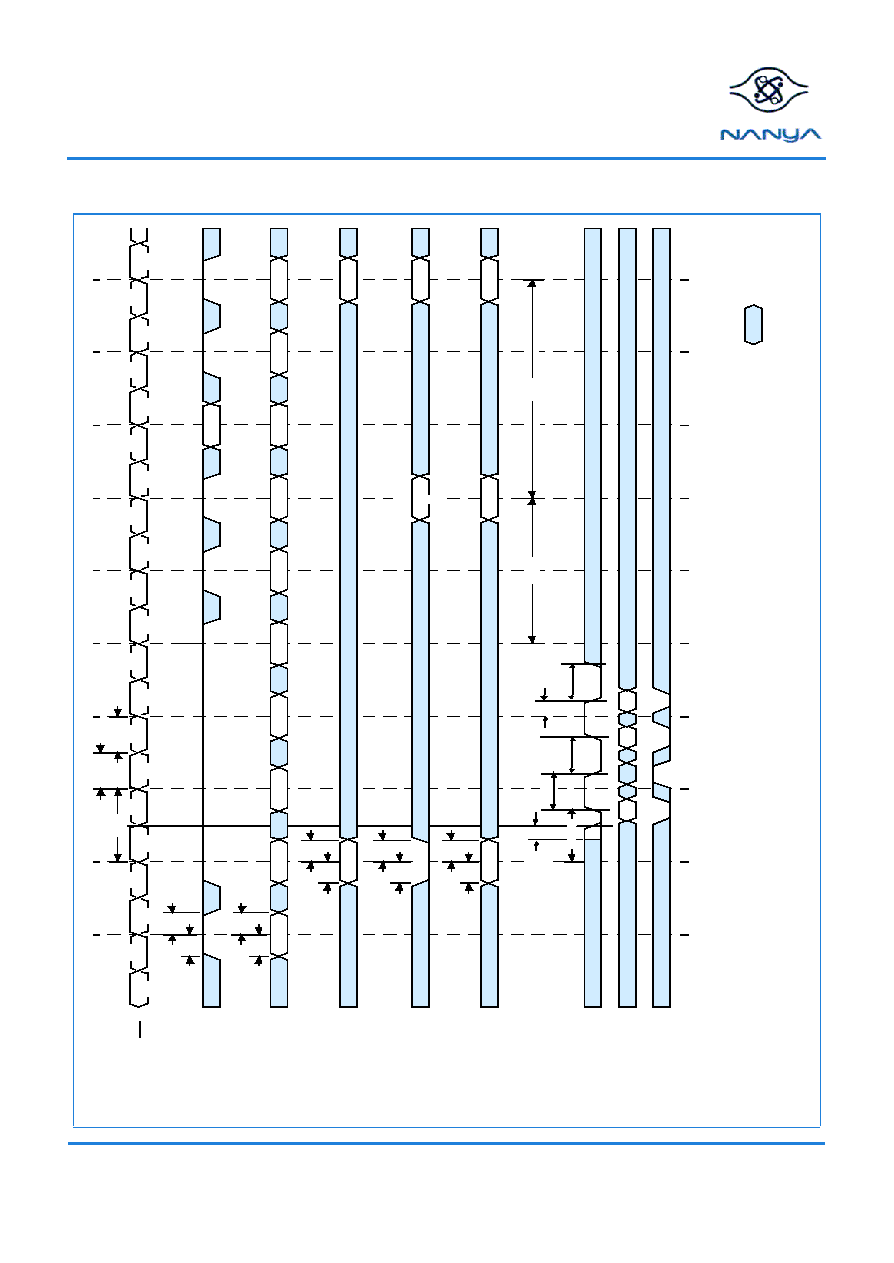
NT5DS64M4AT NT5DS64M4AW
NT5DS32M8AT NT5DS32M8AW
256Mb Double Data Rate SDRAM
REV 1.3
08/2002
74
©
NANYA TECHNOLOGY CORP
. All rights reserved.
NANYA TECHNOLOGY CORP. reserves the right to change Products and Specifications without notice.
Write DM Operation (Burst Length = 4)
t
I
H
t
W
P
S
T
t
D
Q
S
L
t
I
H
t
I
S
t
I
H
t
I
S
t
I
S
t
R
P
t
C
L
t
C
H
t
C
K
N
O
P
N
O
P
N
O
P
P
R
E
N
O
P
N
O
P
A
C
T
N
O
P
N
O
P
W
r
i
t
e
C
O
L
n
R
A
D
I
n
C
K
C
K
C
K
E
C
o
m
m
a
n
d
A
1
0
B
A
0
,
B
A
1
D
Q
S
D
Q
D
M
t
W
R
t
D
Q
S
S
D
o
n
'
t
C
a
r
e
V
A
L
I
D
t
I
H
t
I
S
t
I
H
t
I
S
B
A
x
B
A
R
A
B
A
x
*
A
L
L
B
A
N
K
S
O
N
E
B
A
N
K
D
I
S
A
P
D
I
n
=
d
a
t
a
i
n
f
o
r
c
o
l
u
m
n
n
.
3
s
u
b
s
e
q
u
e
n
t
e
l
e
m
e
n
t
s
o
f
d
a
t
a
i
n
a
r
e
a
p
p
l
i
e
d
i
n
t
h
e
p
r
o
g
r
a
m
m
e
d
o
r
d
e
r
f
o
l
l
o
w
i
n
g
D
I
n
(
t
h
e
s
e
c
o
n
d
e
l
e
m
e
n
t
o
f
t
h
e
4
i
s
m
a
s
k
e
d
)
.
D
I
S
A
P
=
D
i
s
a
b
l
e
A
u
t
o
P
r
e
c
h
a
r
g
e
.
*
=
D
o
n
'
t
c
a
r
e
i
f
A
1
0
i
s
H
i
g
h
a
t
t
h
i
s
p
o
i
n
t
.
P
R
E
=
P
r
e
c
h
a
r
g
e
;
A
C
T
=
A
c
t
i
v
e
;
R
A
=
R
o
w
a
d
d
r
e
s
s
;
B
A
=
B
a
n
k
a
d
d
r
e
s
s
.
N
O
P
c
o
m
m
a
n
d
s
a
r
e
s
h
o
w
n
f
o
r
e
a
s
e
o
f
i
l
l
u
s
t
r
a
t
i
o
n
;
o
t
h
e
r
v
a
l
i
d
c
o
m
m
a
n
d
s
m
a
y
b
e
p
o
s
s
i
b
l
e
a
t
t
h
e
s
e
t
i
m
e
s
.
A
0
-
A
9
,
A
1
1
,
A
1
2
t
D
Q
S
H
t
D
S
H
t
D
Q
S
S
=
m
i
n
.
t
W
P
R
E
S

NT5DS64M4AT NT5DS64M4AW
NT5DS32M8AT NT5DS32M8AW
256Mb Double Data Rate SDRAM
REV 1.3
08/2002
75
©
NANYA TECHNOLOGY CORP
. All rights reserved.
NANYA TECHNOLOGY CORP. reserves the right to change Products and Specifications without notice.
Package Dimensions
(400mil; 66 lead; Thin Small Outline Package)
1
0
.
1
6
±
.
0
.
1
3
1
1
.
7
6
±
0
.
2
0
Lead #1
0.65 Basic
0.30
-
0.08
+ 0.03
0.71REF
Detail A
0.10
Seating Plane
Detail A
0.5
±
0.1
0.05 Min
1
.
2
0
M
a
x
0.25 Basic
Gage Plane
22.22
±
0.10
Units : Millimeters

NT5DS64M4AT NT5DS64M4AW
NT5DS32M8AT NT5DS32M8AW
256Mb Double Data Rate SDRAM
REV 1.3
08/2002
76
©
NANYA TECHNOLOGY CORP
. All rights reserved.
NANYA TECHNOLOGY CORP. reserves the right to change Products and Specifications without notice.
Package Dimensions
(60 balls; 0.8mmx1.0mm Pitch; CSP Package)
1.05
0.80
8.5
1.00
0.50
15.50
2.25
1.60
0.35
1.15
Dia.
0.45
Note : All dimensions are typical unless otherwise stated.
Unit : Millimeters

NT5DS64M4AT NT5DS64M4AW
NT5DS32M8AT NT5DS32M8AW
256Mb Double Data Rate SDRAM
REV 1.3
08/2002
77
©
NANYA TECHNOLOGY CORP
. All rights reserved.
NANYA TECHNOLOGY CORP. reserves the right to change Products and Specifications without notice.
Revision Log
Rev
Contents of Modification
01/01
Preliminary
05/01
Changed to Revision 1.0
12/01
Changed to Revision 1.1
Added CSP ball configuration
Added CSP package dimensions
Removed the QFC function
06/02
Changed to Revision 1.2
Modified I
DD1
from 90mA to 110mA (DDR200) and 110mA to 120mA (DDR266)
Modified I
DD2P
from 15mA to 25mA
Modified I
DD3P
from 15mA to 25mA
Updated I
DD7
to 250mA (DDR200) and 300mA (DDR266)
08/02
Changed to Revision 1.3
Added t
XARD
(Power down exit time) to Power Down Mode Timing Diagram
Added t
XARD
(Power down exit time) to AC Timing Table

Nanya Technology Corporation.
All rights reserved.
Printed in Taiwan, R.O.C. June 2002
The following are trademarks of NANYA TECHNOLOGY CORPORATION in R.O.C , or other countries, or both.
NANYA NANYA logo
Other company, product and service names may be trademarks or service marks of others.
NANYA TECHNOLOGY CORPORATION (NTC) reserves the right to make changes without notice. NTC warrants performance
of its semiconductor products and related software to the specifications applicable at the time of sale in accordance with NTC's
standard warranty. Testing and other quality control techniques are utilize to the extent NTC deems necessary to support this
warranty. Specific testing of all parameters of each device is not necessarily performed, except those mandated by government
requirements.
Certain applications using semiconductor products may involve potential risks of death, personal injury, or severe property or
environmental damage ("Critical Applications").
NTC SEMICONDUCTOR PRODUCTS ARE NOT DESIGNED, INTEND, AUTHORIZED, OR WARRANTED TO BE SUITABLE
FOR USE IN LIFE-SUPPORT APPLICATIONS, DEVICES OR SYSTEMS OR OTHER CRITICAL APPLICATIONS.
Inclusion of NTC products in such applications is understood to be fully at the risk of the customer. Use of NTC products in such
applications requires the written approval of an appropriate NTC officer. Question concerning potential risk applications should
be directed to NTC through a local sales office.
In order to minimize risks associated with the customer's applications, adequate design and operating safeguards should be
provided by customer to minimize the inherent or procedural hazards.
NTC assumes no liability of applications assistance, customer product design, software performance, or infringement of patents
or services described herein. Nor does NTC warrant or represent that any license, either express or implied, is granted under
any patent right, copyright, mask work right, or other intellectual property right of NTC covering or relating to any combination,
machine, or process in which such semiconductor products or services might be or are used.
NANYA TECHNOLOGY CORPORATION
HWA YA Technology Park
669, FU HSING 3rd Rd., Kueishan,
Taoyuan, Taiwan, R.O.C.
The NANYA TECHNOLOGY CORPORATION home page can be found at
http:\\www.nanya.com
©
Æ