
NT5SV32M4CT
NT5SV16M8CT
NT5SV8M16CT
128Mb Synchronous DRAM
REV 1.0
May, 2001
1
©
NANYA TECHNOLOGY CORP
. All rights reserved.
NANYA TECHNOLOGY CORP. reserves the right to change Products and Specifications without notice.
Features
∑ High Performance:
∑ Single Pulsed RAS Interface
∑ Fully Synchronous to Positive Clock Edge
∑ Four Banks controlled by BS0/BS1 (Bank Select)
∑ Programmable CAS Latency: 2, 3
∑ Programmable Burst Length: 1, 2, 4, 8
∑ Programmable Wrap: Sequential or Interleave
∑ Multiple Burst Read with Single Write Option
∑ Automatic and Controlled Precharge Command
∑ Data Mask for Read/Write control (x4, x8)
∑ Dual Data Mask for byte control (x16)
∑ Auto Refresh (CBR) and Self Refresh
∑ Suspend Mode and Power Down Mode
∑ Standard Power operation
∑ 4096 refresh cycles/64ms
∑ Random Column Address every CK (1-N Rule)
∑ Single 3.3V
±
0.3V Power Supply
∑ LVTTL compatible
∑ Package:
54-pin 400 mil TSOP-Type II
Description
The NT5SV32M4CT, NT5SV16M8CT, and NT5SV8M16CT
are four-bank Synchronous DRAMs organized as 8Mbit x 4
I/O x 4 Bank, 4Mbit x 8 I/O x 4 Bank, and 2Mbit x 16 I/O x 4
Bank, respectively. These synchronous devices achieve
high-speed data transfer rates of up to 133MHz by employing
a pipeline chip architecture that synchronizes the output data
to a system clock. The chip is fabricated with NTC's
advanced 128Mbit single transistor CMOS DRAM process
technology.
The device is designed to comply with all JEDEC standards
set for synchronous DRAM products, both electrically and
mechanically. All of the control, address, and data input/out-
put (I/O or DQ) circuits are synchronized with the positive
edge of an externally supplied clock.
RAS, CAS, WE, and CS are pulsed signals which are exam-
ined at the positive edge of each externally applied clock
(CK). Internal chip operating modes are defined by combina-
tions of these signals and a command decoder initiates the
necessary timings for each operation. A fourteen bit address
bus accepts address data in the conventional RAS/CAS mul-
tiplexing style. Twelve row addresses (A0-A11) and two bank
select addresses (BS0, BS1) are strobed with RAS. Eleven
column addresses (A0-A9, A11) plus bank select addresses
and A10 are strobed with CAS. Column address A11 is
dropped on the x8 device, and column addresses A11 and
A9 are dropped on the x16 device.
Prior to any access operation, the CAS latency, burst length,
and burst sequence must be programmed into the device by
address inputs A0-A11, BS0, BS1 during a mode register set
cycle. In addition, it is possible to program a multiple burst
sequence with single write cycle for write through cache oper-
ation.
Operating the four memory banks in an interleave fashion
allows random access operation to occur at a higher rate
than is possible with standard DRAMs. A sequential and gap-
less data rate of up to 133MHz is possible depending on
burst length, CAS latency, and speed grade of the device.
Auto Refresh (CBR) and Self Refresh operation are sup-
ported.
-7K
3
CL=2
-75B,
CL=3
-8B,
CL=2
Units
f
CK
Clock
Frequency
133
133
100
MHz
t
CK
Clock Cycle
7.5
7.5
10
ns
t
AC
Clock Access
Time
1
--
--
--
ns
t
AC
Clock Access
Time
2
5.4
5.4
6
ns
1. Terminated load. See AC Characteristics on page 37.
2. Unterminated load. See AC Characteristics on page 37.
3. t
RP
= t
RCD
= 2 CKs

NT5SV32M4CT
NT5SV16M8CT
NT5SV8M16CT
128Mb Synchronous DRAM
REV 1.0
May, 2001
2
©
NANYA TECHNOLOGY CORP
. All rights reserved.
NANYA TECHNOLOGY CORP. reserves the right to change Products and Specifications without notice.
Pin Assignments for Planar Components
(Top View)
54-pin Plastic TSOP(II) 400 mil
8Mbit x 4 I/O x 4 Bank
NT5SV32M4CT
1
2
3
4
5
6
9
10
11
12
13
14
7
8
15
16
17
18
19
20
21
22
54
53
52
51
50
49
46
45
44
43
42
41
48
47
40
39
38
37
36
35
34
33
V
DD
NC
V
DDQ
NC
DQ0
V
SSQ
V
DDQ
NC
DQ1
V
SSQ
NC
V
DD
NC
NC
NC
WE
CAS
RAS
CS
BS0
BS1
V
SS
NC
V
SSQ
NC
DQ3
V
DDQ
V
SSQ
NC
DQ2
V
DDQ
NC
V
SS
NC
NC
NC
DQM
CK
CKE
NC
A11
A9
23
24
25
32
31
30
A10/AP
A0
A1
A2
A8
A7
A6
A5
26
27
29
28
A3
V
DD
A4
V
SS
V
DD
DQ0
V
DDQ
NC
DQ1
V
SSQ
V
DDQ
NC
DQ3
V
SSQ
NC
V
DD
NC
DQ2
NC
W E
CAS
RAS
CS
BS0
BS1
A10/AP
A0
A1
A2
A3
V
DD
V
SS
DQ7
V
SSQ
NC
DQ6
V
DDQ
V
SSQ
NC
DQ4
V
DDQ
NC
V
SS
NC
DQ5
NC
DQM
CK
CKE
NC
A11
A9
A8
A7
A6
A5
A4
V
SS
V
D D
DQ0
V
DDQ
DQ1
DQ2
V
SSQ
V
DDQ
DQ5
DQ6
V
SSQ
DQ7
V
D D
DQ3
DQ4
LDQM
WE
CAS
RAS
CS
BS0
BS1
A10/AP
A0
A1
A2
A3
V
DD
V
SS
DQ15
V
SSQ
DQ14
DQ13
V
DDQ
V
SSQ
DQ10
DQ9
V
DDQ
DQ8
V
SS
DQ12
DQ11
NC
UDQM
CK
CKE
NC
A11
A9
A8
A7
A6
A5
A4
V
SS
2Mbit x 16 I/O x 4 Bank
NT5SV8M16CT
4Mbit x 8 I/O x 4 Bank
NT5SV16M8CT

NT5SV32M4CT
NT5SV16M8CT
NT5SV8M16CT
128Mb Synchronous DRAM
REV 1.0
May, 2001
3
©
NANYA TECHNOLOGY CORP
. All rights reserved.
NANYA TECHNOLOGY CORP. reserves the right to change Products and Specifications without notice.
Pin Description
CK
Clock Input
DQ0-DQ15
Data Input/Output
CKE
Clock Enable
DQM, LDQM, UDQM
Data Mask
CS
Chip Select
V
DD
Power (+3.3V)
RAS
Row Address Strobe
V
SS
Ground
CAS
Column Address Strobe
V
DDQ
Power for DQs (+3.3V)
WE
Write Enable
V
SSQ
Ground for DQs
BS1, BS0
Bank Select
NC
No Connection
A0 - A11
Address Inputs
--
--
Input/Output Functional Description
Symbol
Type
Polarity
Function
CLK
Input
Positive
Edge
The system clock input. All of the SDRAM inputs are sampled on the rising edge of the clock.
CKE
Input
Active High
Activates the CLK signal when high and deactivates the CLK signal when low. By deactivating the
clock, CKE low initiates the Power Down mode, Suspend mode, or the Self Refresh mode.
CS
Input
Active Low
CS enables the command decoder when low and disables the command decoder when high. When the
command decoder is disabled, new commands are ignored but previous operations continue.
RAS, CAS,
WE
Input
Active Low
When sampled at the positive rising edge of the clock, CAS , RAS , and WE define the operation to be
executed by the SDRAM.
BS0, BS1
Input
--
Selects which bank is to be active.
A0 - A11
Input
--
During a Bank Activate command cycle, A0-A11 defines the row address (RA0-RA11) when sampled at
the rising clock edge.
During a Read or Write command cycle, A0-A9 and A11 defines the column address (CA0-CA9, CA11)
when sampled at the rising clock edge.
A10 is used to invoke auto-precharge operation at the end of the burst read or write cycle. If A10 is
high, auto-precharge is selected and BS0, BS1 defines the bank to be precharged. If A10 is low, auto-
precharge is disabled.
During a Precharge command cycle, A10 is used in conjunction with BS0, BS1 to control which bank(s)
to precharge. If A10 is high, all banks will be precharged regardless of the state of BS. If A10 is low,
then BS0 and BS1 are used to define which bank to precharge.
DQ0 - DQ15
Input-
Output
--
Data Input/Output pins operate in the same manner as on conventional DRAMs.
DQM
LDQM
UDQM
Input
Active High
The Data Input/Output mask places the DQ buffers in a high impedance state when sampled high. In
x16 products, LDQM and UDQM control the lower and upper byte I/O buffers, respectively. In Read
mode, DQM has a latency of two clock cycles and controls the output buffers like an output enable.
DQM low turns the output buffers on and DQM high turns them off. In Write mode, DQM has a latency
of zero and operates as a word mask by allowing input data to be written if it is low but blocks the write
operation if DQM is high.
V
D D
, V
SS
Supply
--
Power and ground for the input buffers and the core logic.
V
DDQ
V
SSQ
Supply
--
Isolated power supply and ground for the output buffers to provide improved noise immunity.

NT5SV32M4CT
NT5SV16M8CT
NT5SV8M16CT
128Mb Synchronous DRAM
REV 1.0
May, 2001
4
©
NANYA TECHNOLOGY CORP
. All rights reserved.
NANYA TECHNOLOGY CORP. reserves the right to change Products and Specifications without notice.
Ordering Information
Organization
Part Number
Speed Grade
Power
Supply
Package
Clock Frequency@CAS Latency
Note
32M x 4
NT5SV32M4CT-7K
143MHz@CL3
133MHz@CL2
PC133 , PC100
3.3 V
400mil 54-PIN
TSOP II
NT5SV32M4CT-75B
133MHz@CL3
100MHz@CL2
PC133 , PC100
NT5SV32M4CT-8B
125MHz@CL3
100MHz@CL2
PC100
16M x 8
NT5SV16M8CT-7K
143MHz@CL3
133MHz@CL2
PC133 , PC100
NT5SV16M8CT-75B
133MHz@CL3
100MHz@CL2
PC133 , PC100
NT5SV16M8CT-8B
125MHz@CL3
100MHz@CL2
PC100
8M x 16
NT5SV8M16CT-7K
143MHz@CL3
133MHz@CL2
PC133 , PC100
NT5SV8M16CT-75B
133MHz@CL3
100MHz@CL2
PC133 , PC100
NT5SV8M16CT-8B
125MHz@CL3
100MHz@CL2
PC100

NT5SV32M4CT
NT5SV16M8CT
NT5SV8M16CT
128Mb Synchronous DRAM
REV 1.0
May, 2001
5
©
NANYA TECHNOLOGY CORP
. All rights reserved.
NANYA TECHNOLOGY CORP. reserves the right to change Products and Specifications without notice.
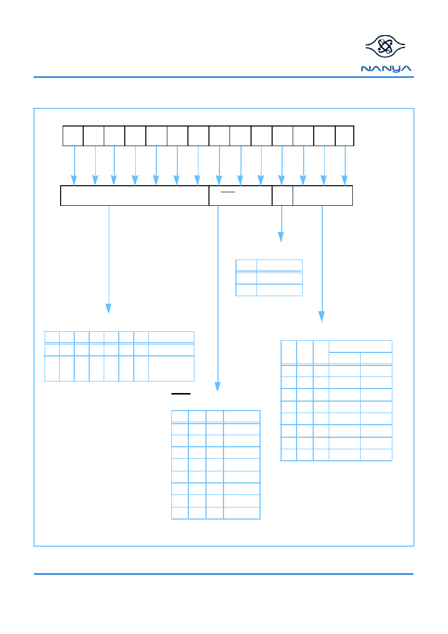
Block Diagram
DQ
0
DQ
X
D
a
t
a
I
n
p
u
t
/
O
u
t
p
u
t
B
u
f
f
e
r
s
CKE Buffer
CLK Buffer
CKE
CLK
CS
RAS
CAS
DQM
WE
C
o
m
m
a
n
d
D
e
c
o
d
e
r
M
o
d
e
R
e
g
i
s
t
e
r
C
o
u
n
t
e
r
C
o
l
u
m
n
A
d
d
r
e
s
s
C
o
u
n
t
e
r
R
e
f
r
e
s
h
A1
A2
A3
A4
A5
A6
A7
A10
A8
A9
A0
A11
Sense Amplifiers
Memory Bank 1
Cell Array
R
o
w
D
e
c
o
d
e
r
A
d
d
r
e
s
s
B
u
f
f
e
r
s
(
1
4
)
Column Decoder
Sense Amplifiers
Memory Bank 3
Cell Array
R
o
w
D
e
c
o
d
e
r
Column Decoder
Sense Amplifiers
Memory Bank 0
Cell Array
R
o
w
D
e
c
o
d
e
r
Column Decoder
Sense Amplifiers
Memory Bank 2
Cell Array
R
o
w
D
e
c
o
d
e
r
Column Decoder
D
a
t
a
C
o
n
t
r
o
l
C
i
r
c
u
i
t
r
y
BS1
BS0
C
o
n
t
r
o
l
S
i
g
n
a
l
G
e
n
e
r
a
t
o
r
Cell Array, per bank, for 8Mb x 4 DQ: 4096 Row x 2048 Col x 4 DQ (DQ0-DQ3).
Cell Array, per bank, for 4Mb x 8 DQ: 4096 Row x 1024 Col x 8 DQ (DQ0-DQ7)
.
Cell Array, per bank, for 2Mb x 16 DQ: 4096 Row x 512 Col x 16 DQ (DQ0-DQ15).

NT5SV32M4CT
NT5SV16M8CT
NT5SV8M16CT
128Mb Synchronous DRAM
REV 1.0
May, 2001
6
©
NANYA TECHNOLOGY CORP
. All rights reserved.
NANYA TECHNOLOGY CORP. reserves the right to change Products and Specifications without notice.
Power On and Initialization
The default power on state of the mode register is supplier specific and may be undefined. The following power on and initializa-
tion sequence guarantees the device is preconditioned to each users specific needs.
Like a conventional DRAM, the Synchronous DRAM must be powered up and initialized in a predefined manner. During power
on, all V
DD
and V
DDQ
pins must be built up simultaneously to the specified voltage when the input signals are held in the "NOP"
state. The power on voltage must not exceed V
DD
+0.3V on any of the input pins or V
DD
supplies. The CK signal must be started
at the same time. After power on, an initial pause of 200
µ
s is required followed by a precharge of all banks using the precharge
command. To prevent data contention on the DQ bus during power on, it is required that the DQM and CKE pins be held high
during the initial pause period. Once all banks have been precharged, the Mode Register Set Command must be issued to ini-
tialize the Mode Register. A minimum of two Auto Refresh cycles (CBR) are also required. These may be done before or after
programming the Mode Register. Failure to follow these steps may lead to unpredictable start-up modes.
Programming the Mode Register
For application flexibility, CAS latency, burst length, burst sequence, and operation type are user defined variables and must be
programmed into the SDRAM Mode Register with a single Mode Register Set Command. Any content of the Mode Register can
be altered by re-executing the Mode Register Set Command. If the user chooses to modify only a subset of the Mode Register
variables, all four variables must be redefined when the Mode Register Set Command is issued.
After initial power up, the Mode Register Set Command must be issued before read or write cycles may begin. All banks must
be in a precharged state and CKE must be high at least one cycle before the Mode Register Set Command can be issued. The
Mode Register Set Command is activated by the low signals of RAS, CAS, CS, and WE at the positive edge of the clock. The
address input data during this cycle defines the parameters to be set as shown in the Mode Register Operation table. A new
command may be issued following the mode register set command once a delay equal to t
RSC
has elapsed.
CAS Latency
The CAS latency is a parameter that is used to define the delay from when a Read Command is registered on a rising clock
edge to when the data from that Read Command becomes available at the outputs. The CAS latency is expressed in terms of
clock cycles and can have a value of 2 or 3 cycles. The value of the CAS latency is determined by the speed grade of the
device and the clock frequency that is used in the application. A table showing the relationship between the CAS latency, speed
grade, and clock frequency appears in the Electrical Characteristics section of this document. Once the appropriate CAS
latency has been selected it must be programmed into the mode register after power up, for an explanation of this procedure
see Programming the Mode Register in the previous section.
NT5SV32M4CT
NT5SV16M8CT
NT5SV8M16CT
128Mb Synchronous DRAM
REV 1.0
May, 2001
7
©
NANYA TECHNOLOGY CORP
. All rights reserved.
NANYA TECHNOLOGY CORP. reserves the right to change Products and Specifications without notice.
Mode Register Operation (Address Input For Mode Set)
A11
A3
A4
A2
A1
A0
A10
A9
A8
A7
A6
A5
Address
BT
Burst Length
CAS Latency
Mode
CAS Latency
M6
M5
M4
Latency
0
0
0
Reserved
0
0
1
Reserved
0
1
0
2
0
1
1
3
1
0
0
Reserved
1
0
1
Reserved
1
1
0
Reserved
1
1
1
Reserved
Burst Length
M2
M1
M0
Length
Sequential Interleave
0
0
0
1
1
0
0
1
2
2
0
1
0
4
4
0
1
1
8
8
1
0
0
Reserved Reserved
1
0
1
Reserved Reserved
1
1
0
Reserved Reserved
1
1
1
Reserved Reserved
Burst Type
M3
Type
0
Sequential
1
Interleave
Operation Mode
M1 3 M12 M11 M10 M9
M8
M7
Mode
0
0
0
0
0
0
0
Normal
0
0
0
0
1
0
0
Multiple Burst
with
Single Write
Operation Mode
BS1
Bus (Ax)
Register(Mx)
BS0

NT5SV32M4CT
NT5SV16M8CT
NT5SV8M16CT
128Mb Synchronous DRAM
REV 1.0
May, 2001
8
©
NANYA TECHNOLOGY CORP
. All rights reserved.
NANYA TECHNOLOGY CORP. reserves the right to change Products and Specifications without notice.
Burst Mode Operation
Burst mode operation is used to provide a constant flow of data to memory locations (write cycle), or from memory locations
(read cycle). There are three parameters that define how the burst mode will operate. These parameters include burst
sequence, burst length, and operation mode. The burst sequence and burst length are programmable, and are determined by
address bits A0 - A3 during the Mode Register Set command. Operation mode is also programmable and is set by address bits
A7 - A11, BS0, and BS1.
The burst type is used to define the order in which the burst data will be delivered or stored to the SDRAM. Two types of burst
sequences are supported, sequential and interleaved. See the table below.
The burst length controls the number of bits that will be output after a Read Command, or the number of bits to be input after a
Write Command. The burst length can be programmed to have values of 1, 2, 4, 8 (actual page length is dependent on organi-
zation: x4, x8, or x16).
Burst operation mode can be normal operation or multiple burst with single write operation. Normal operation implies that the
device will perform burst operations on both read and write cycles until the desired burst length is satisfied. Multiple burst with
single write operation was added to support Write Through Cache operation. Here, the programmed burst length only applies to
read cycles. All write cycles are single write operations when this mode is selected.
Note: Page length is a function of I/O organization and column addressing.
x4 organization (CA0-CA9, CA11); Page Length = 2048 bits
x8 organization (CA0-CA9); Page Length = 1024 bits
x16 organization (CA0-CA8); Page Length = 512 bits
Burst Length and Sequence
Burst Length
Starting Address (A2 A1 A0)
Sequential Addressing (decimal)
Interleave Addressing (decimal)
2
x x 0
0, 1
0, 1
x x 1
1, 0
1, 0
4
x 0 0
0, 1, 2, 3
0, 1, 2, 3
x 0 1
1, 2, 3, 0
1, 0, 3, 2
x 1 0
2, 3, 0, 1
2, 3, 0, 1
x 1 1
3, 0, 1, 2
3, 2, 1, 0
8
0 0 0
0, 1, 2, 3, 4, 5, 6, 7
0, 1, 2, 3, 4, 5, 6, 7
0 0 1
1, 2, 3, 4, 5, 6, 7, 0
1, 0, 3, 2, 5, 4, 7, 6
0 1 0
2, 3, 4, 5, 6, 7, 0, 1
2, 3, 0, 1, 6, 7, 4, 5
0 1 1
3, 4, 5, 6, 7, 0, 1, 2
3, 2, 1, 0, 7, 6, 5, 4
1 0 0
4, 5, 6, 7, 0, 1, 2, 3
4, 5, 6, 7, 0, 1, 2, 3
1 0 1
5, 6, 7, 0, 1, 2, 3, 4
5, 4, 7, 6, 1, 0, 3, 2
1 1 0
6, 7, 0, 1, 2, 3, 4, 5
6, 7, 4, 5, 2, 3, 0, 1
1 1 1
7, 0, 1, 2, 3, 4, 5, 6
7, 6, 5, 4, 3, 2, 1, 0

NT5SV32M4CT
NT5SV16M8CT
NT5SV8M16CT
128Mb Synchronous DRAM
REV 1.0
May, 2001
9
©
NANYA TECHNOLOGY CORP
. All rights reserved.
NANYA TECHNOLOGY CORP. reserves the right to change Products and Specifications without notice.
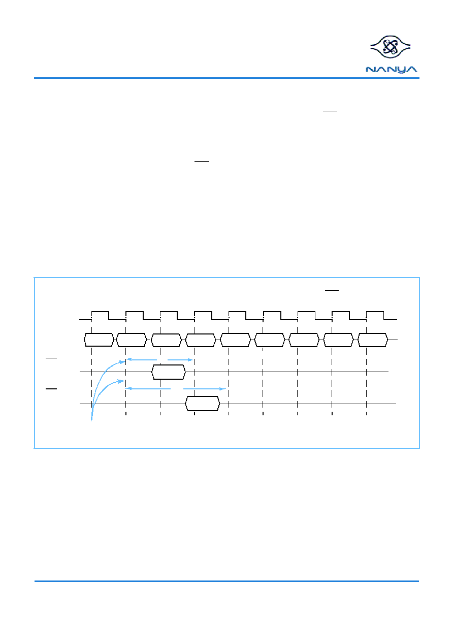
Bank Activate Command
In relation to the operation of a fast page mode DRAM, the Bank Activate command correlates to a falling RAS signal.
The Bank
Activate command is issued by holding CAS and WE high with CS and RAS low at the rising edge of the clock. The Bank Select
address BS0 - BS1 is used to select the desired bank. The row address A0 - A11 is used to determine which row to activate in
the selected bank.
The Bank Activate command must be applied before any Read or Write operation can be executed. The delay from when the
Bank Activate command is applied to when the first read or write operation can begin must meet or exceed the RAS to CAS
delay time (t
RCD
). Once a bank has been activated it must be precharged before another Bank Activate command can be
applied to the same bank. The minimum time interval between successive Bank Activate commands to the same bank is deter-
mined by the RAS cycle time of the device (t
RC
). The minimum time interval between interleaved Bank Activate commands
(Bank A to Bank B and vice versa) is the Bank to Bank delay time (t
RRD
). The maximum time that each bank can be held active
is specified as t
RAS(max)
.
Bank Select
The Bank Select inputs, BS0 and BS1, determine the bank to be used during a Bank Activate, Precharge, Read, or Write oper-
ation.
Bank Activate Command Cycle
Bank Selection Bits
BS0
BS1
Bank
0
0
Bank 0
1
0
Bank 1
0
1
Bank 2
1
1
Bank 3
ADDRESS
CK
T0
T2
T1
T3
Tn
Tn+1
Tn+2
Tn+3
COMMAND
NOP
NOP
NOP
NOP
Bank A
Row Addr.
Bank A
Activate
Write A
with Auto
Bank A
Col. Addr.
. . . . . . . . . .
. . . . . . . . . .
. . . . . . . . . .
Bank B
Activate
Bank A
Row Addr.
Bank A
Activate
RAS-CAS delay (
t
RCD
)
: "H" or "L"
RAS Cycle time (
t
RC
)
Precharge
RAS - RAS delay time (
t
RRD
)
Bank B
Row Addr.
(CAS Latency = 3, t
RCD
= 3)

NT5SV32M4CT
NT5SV16M8CT
NT5SV8M16CT
128Mb Synchronous DRAM
REV 1.0
May, 2001
10
©
NANYA TECHNOLOGY CORP
. All rights reserved.
NANYA TECHNOLOGY CORP. reserves the right to change Products and Specifications without notice.
Read and Write Access Modes
After a bank has been activated, a read or write cycle can be executed. This is accomplished by setting RAS high and CAS low
at the clock's rising edge after the necessary RAS to CAS delay (t
RCD
). WE must also be defined at this time to determine
whether the access cycle is a read operation (WE high), or a write operation (WE low). The address inputs determine the start-
ing column address.
The SDRAM provides a wide variety of fast access modes. A single Read or Write Command will initiate a serial read or write
operation on successive clock cycles up to 133MHz. The number of serial data bits for each access is equal to the burst length,
which is programmed into the Mode Register.
Similar to Page Mode of conventional DRAMs, a read or write cycle can not begin until the sense amplifiers latch the selected
row address information. The refresh period (t
REF
) is what limits the number of random column accesses to an activated bank.
A new burst access can be done even before the previous burst ends. The ability to interrupt a burst operation at every clock
cycle is supported; this is referred to as the 1-N rule. When the previous burst is interrupted by another Read or Write Com-
mand, the remaining addresses are overridden by the new address.
Precharging an active bank after each read or write operation is not necessary providing the same row is to be accessed again.
To perform a read or write cycle to a different row within an activated bank, the bank must be precharged and a new Bank Acti-
vate command must be issued. When more than one bank is activated, interleaved (ping pong) bank Read or Write operations
are possible. By using the programmed burst length and alternating the access and precharge operations between multiple
banks, fast and seamless data access operation among many different pages can be realized. When multiple banks are acti-
vated, column to column interleave operation can be done between different pages. Finally, Read or Write Commands can be
issued to the same bank or between active banks on every clock cycle.
NT5SV32M4CT
NT5SV16M8CT
NT5SV8M16CT
128Mb Synchronous DRAM
REV 1.0
May, 2001
11
©
NANYA TECHNOLOGY CORP
. All rights reserved.
NANYA TECHNOLOGY CORP. reserves the right to change Products and Specifications without notice.
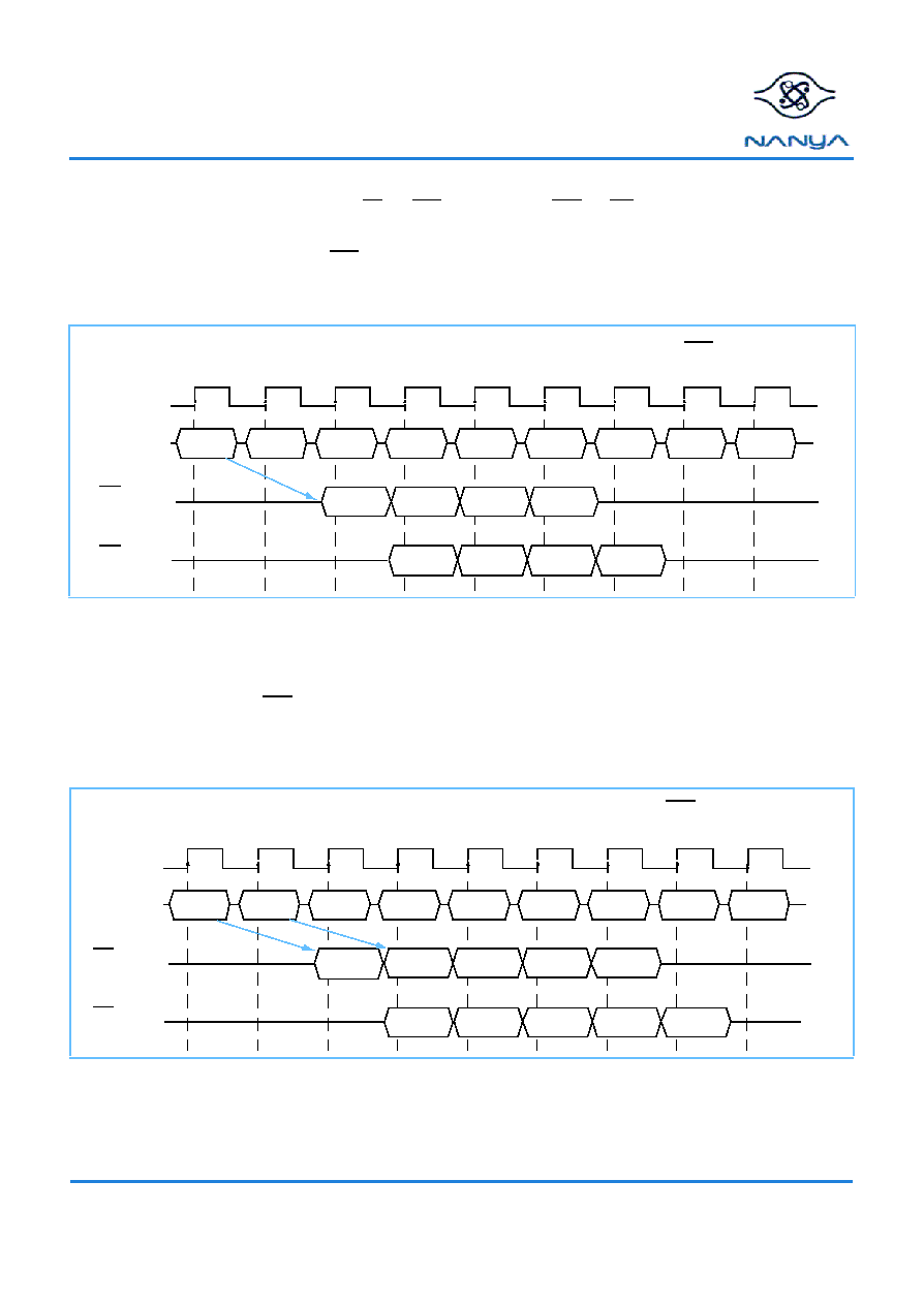
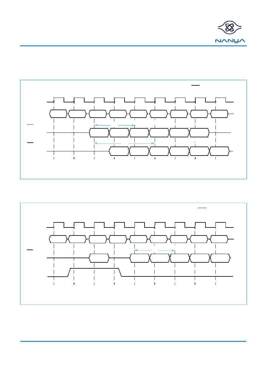
Burst Read Command
The Burst Read command is initiated by having CS and CAS low while holding RAS and WE high at the rising edge of the clock.
The address inputs determine the starting column address for the burst, the Mode Register sets the type of burst (sequential or
interleave) and the burst length (1, 2, 4, 8). The delay from the start of the command to when the data from the first cell appears
on the outputs is equal to the value of the CAS latency that is set in the Mode Register.
Read Interrupted by a Read
A Burst Read may be interrupted before completion of the burst by another Read Command, with the only restriction being that
the interval that separates the commands must be at least one clock cycle. When the previous burst is interrupted, the remain-
ing addresses are overridden by the new address with the full burst length. The data from the first Read Command continues to
appear on the outputs until the CAS latency from the interrupting Read Command is satisfied, at this point the data from the
interrupting Read Command appears.
Burst Read Operation
Read Interrupted by a Read
COMMAND
READ A
NOP
NOP
NOP
NOP
NOP
NOP
NOP
DOUT A
0
CAS latency = 2
t
CK3
,
DQs
CAS latency = 3
DOUT A
1
DOUT A
2
DOUT A
3
NOP
CK
T0
T2
T1
T3
T4
T5
T6
T7
T8
t
CK2
,
DQs
DOUT A
0
DOUT A
1
DOUT A
2
DOUT A
3
(Burst Length = 4, CAS latency = 2, 3)
COMMAND
READ A
READ B
NOP
NOP
NOP
NOP
NOP
NOP
t
CK2
,
DQs
CAS latency = 2
t
CK3
,
DQs
CAS latency = 3
NOP
CK
T0
T2
T1
T3
T4
T5
T6
T7
T8
DOUT B
0
DOUT B
1
DOUT B
2
DOUT B
3
DOUT A
0
DOUT B
0
DOUT B
1
DOUT B
2
DOUT B
3
DOUT A
0
(Burst Length = 4, CAS latency = 2, 3)
NT5SV32M4CT
NT5SV16M8CT
NT5SV8M16CT
128Mb Synchronous DRAM
REV 1.0
May, 2001
12
©
NANYA TECHNOLOGY CORP
. All rights reserved.
NANYA TECHNOLOGY CORP. reserves the right to change Products and Specifications without notice.
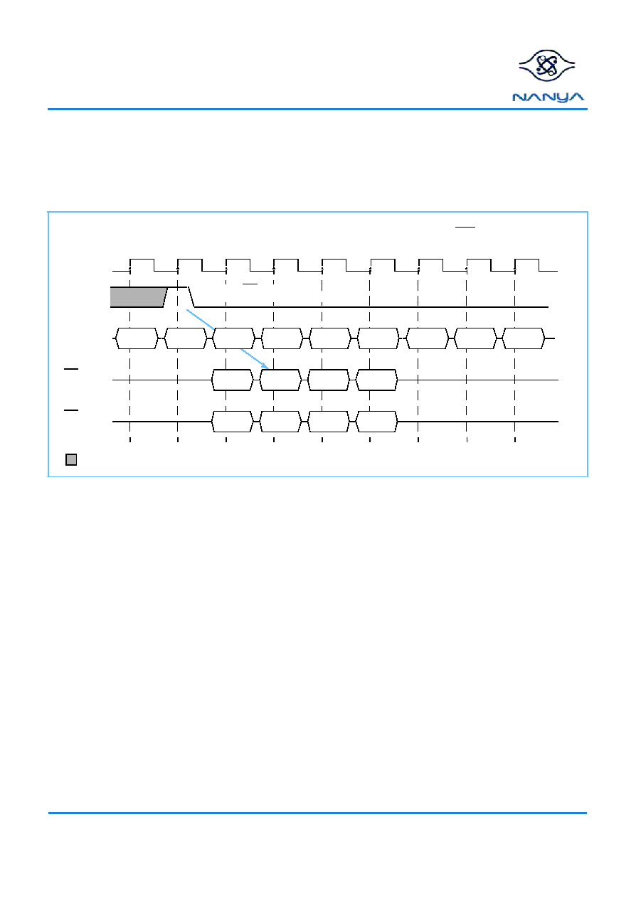
Read Interrupted by a Write
To interrupt a burst read with a Write Command, DQM may be needed to place the DQs (output drivers) in a high impedance
state to avoid data contention on the DQ bus. If a Read Command will issue data on the first or second clocks cycles of the write
operation, DQM is needed to insure the DQs are tri-stated. After that point the Write Command will have control of the DQ bus.
Minimum Read to Write Interval
COMMAND
NOP
NOP
READ A
WRITE A
NOP
NOP
NOP
DQM
DIN A
0
DIN A
1
DIN A
2
DIN A
3
: "H" or "L"
DIN A
0
DIN A
1
DIN A
2
DIN A
3
t
CK2
,
DQs
CAS latency = 2
t
CK3
,
DQs
CAS latency = 3
CK
T0
T2
T1
T3
T4
T5
T6
T7
T8
NOP
NOP
(Burst Length = 4, CAS latency = 2, 3)
DQM high for CAS latency = 2 only.
Required to mask first bit of READ data.
NT5SV32M4CT
NT5SV16M8CT
NT5SV8M16CT
128Mb Synchronous DRAM
REV 1.0
May, 2001
13
©
NANYA TECHNOLOGY CORP
. All rights reserved.
NANYA TECHNOLOGY CORP. reserves the right to change Products and Specifications without notice.
Non-Minimum Read to Write Interval
COMMAND
NOP
NOP
READ A
WRITE A
NOP
NOP
NOP
DQM
DIN A
0
DIN A
1
DIN A
2
DIN A
3
DIN A
0
DIN A
1
DIN A
2
DIN A
3
t
CK2
,
DQs
CAS latency = 2
t
CK3
,
DQs
CAS latency = 3
CK
T0
T2
T1
T3
T4
T5
T6
T7
T8
NOP
NOP
CL = 3: DQM needed to
mask first bit of READ data.
CL = 2: DQM needed to mask
first, second bit of READ data.
(Burst Length = 4, CAS latency = 2, 3)
: DQM high for CAS latency = 2
: DQM high for CAS latency = 3

NT5SV32M4CT
NT5SV16M8CT
NT5SV8M16CT
128Mb Synchronous DRAM
REV 1.0
May, 2001
14
©
NANYA TECHNOLOGY CORP
. All rights reserved.
NANYA TECHNOLOGY CORP. reserves the right to change Products and Specifications without notice.
Burst Write Command
The Burst Write command is initiated by having CS, CAS, and WE low while holding RAS high at the rising edge of the clock.
The address inputs determine the starting column address. There is no CAS latency required for burst write cycles. Data for the
first burst write cycle must be applied on the DQ pins on the same clock cycle that the Write Command is issued. The remaining
data inputs must be supplied on each subsequent rising clock edge until the burst length is completed. When the burst has fin-
ished, any additional data supplied to the DQ pins will be ignored.
Write Interrupted by a Write
A burst write may be interrupted before completion of the burst by another Write Command. When the previous burst is inter-
rupted, the remaining addresses are overridden by the new address and data will be written into the device until the pro-
grammed burst length is satisfied.
Burst Write Operation
Write Interrupted by a Write
COMMAND
NOP
WRITE A
NOP
NOP
NOP
NOP
NOP
NOP
DQs
DIN A
0
DIN A
1
DIN A
2
DIN A
3
NOP
CK
T0
T2
T1
T3
T4
T5
T6
T7
T8
Extra data is masked.
The first data element and the Write
are registered on the same clock edge.
(
Burst Length = 4, CAS latency = 2, 3)
: "H" or "L"
COMMAND
NOP
WRITE A
WRITE B
NOP
NOP
NOP
NOP
NOP
DQs
DIN A
0
DIN B
0
DIN B
1
DIN B
2
NOP
DIN B
3
CK
T0
T2
T1
T3
T4
T5
T6
T7
T8
1 CK Interval
(Burst Length = 4, CAS latency = 2, 3)

NT5SV32M4CT
NT5SV16M8CT
NT5SV8M16CT
128Mb Synchronous DRAM
REV 1.0
May, 2001
15
©
NANYA TECHNOLOGY CORP
. All rights reserved.
NANYA TECHNOLOGY CORP. reserves the right to change Products and Specifications without notice.
Write Interrupted by a Read
A Read Command will interrupt a burst write operation on the same clock cycle that the Read Command is registered. The DQs
must be in the high impedance state at least one cycle before the interrupting read data appears on the outputs to avoid data
contention. When the Read Command is registered, any residual data from the burst write cycle will be ignored. Data that is
presented on the DQ pins before the Read Command is initiated will actually be written to the memory.
Minimum Write to Read Interval
COMMAND
NOP
WRITE A
READ B
NOP
NOP
NOP
NOP
NOP
NOP
t
CK2
,
DQs
CAS latency = 2
DIN A
0
t
CK3
,
DQs
CAS latency = 3
DIN A
0
CK
T0
T2
T1
T3
T4
T5
T6
T7
T8
Input data for the Write is masked.
Input data must be removed from the DQs at least one clock
cycle before the Read data appears on the outputs to avoid
data contention.
DOUT B
0
DOUT B
1
DOUT B
2
DOUT B
3
DOUT B
0
DOUT B
1
DOUT B
2
DOUT B
3
(Burst Length = 4, CAS latency = 2, 3)
: "H" or "L"

NT5SV32M4CT
NT5SV16M8CT
NT5SV8M16CT
128Mb Synchronous DRAM
REV 1.0
May, 2001
16
©
NANYA TECHNOLOGY CORP
. All rights reserved.
NANYA TECHNOLOGY CORP. reserves the right to change Products and Specifications without notice.
Non-Minimum Write to Read Interval
COMMAND
WRITE A
READ B
NOP
NOP
NOP
NOP
NOP
NOP
t
CK2
,
DQs
CAS latency = 2
DIN A
0
t
CK3
,
DQs
CAS latency = 3
DIN A
0
CK
T0
T2
T1
T3
T4
T5
T6
T7
T8
Input data for the Write is masked.
Input data must be removed from the DQs at least one clock
cycle before the Read data appears on the outputs to avoid
data contention.
DOUT B
0
DOUT B
1
DOUT B
2
DOUT B
3
DOUT B
0
DOUT B
1
DOUT B
2
DOUT B
3
NOP
DIN A
1
DIN A
1
(Burst Length = 4, CAS latency = 2, 3)
: "H" or "L"
NT5SV32M4CT
NT5SV16M8CT
NT5SV8M16CT
128Mb Synchronous DRAM
REV 1.0
May, 2001
17
©
NANYA TECHNOLOGY CORP
. All rights reserved.
NANYA TECHNOLOGY CORP. reserves the right to change Products and Specifications without notice.
Auto-Precharge Operation
Before a new row in an active bank can be opened, the active bank must be precharged using either the Precharge Command
or the auto-precharge function. When a Read or a Write Command is given to the SDRAM, the CAS timing accepts one extra
address, column address A10, to allow the active bank to automatically begin precharge at the earliest possible moment during
the burst read or write cycle. If A10 is low when the Read or Write Command is issued, then normal Read or Write burst opera-
tion is executed and the bank remains active at the completion of the burst sequence. If A10 is high when the Read or Write
Command is issued, then the auto-precharge function is engaged. During auto-precharge, a Read Command will execute as
normal with the exception that the active bank will begin to precharge before all burst read cycles have been completed.
Regardless of burst length, the precharge will begin (CAS latency - 1) clocks prior to the last data output. Auto-precharge can
also be implemented during Write commands.
A Read or Write Command without auto-precharge can be terminated in the midst of a burst operation. However, a Read or
Write Command with auto-precharge cannot be interrupted by a command to the same bank. Therefore use of a Read, Write, or
Precharge Command to the same bank is prohibited during a read or write cycle with auto-precharge until the entire burst oper-
ation is completed. Once the precharge operation has started the bank cannot be reactivated until the Precharge time (t
RP
) has
been satisfied.
When using the Auto-precharge Command, the interval between the Bank Activate Command and the beginning of the internal
precharge operation must satisfy t
RAS(min)
. If this interval does not satisfy t
RAS(min)
then t
RCD
must be extended.
Burst Read with Auto-Precharge
COMMAND
NOP
NOP
NOP
NOP
READ A
Auto-Precharge
t
RP
CK
T0
T2
T1
T3
T4
T5
T6
T7
T8
NOP
NOP
NOP
t
RP
*
*
t
CK2
,
DQs
CAS latency = 2
t
CK3
,
DQs
CAS latency = 3
Begin Auto-precharge
*
Bank can be reactivated at completion of t
RP
.
DOUT A
0
DOUT A
0
NOP
t
RP
is a function of clock cycle time and speed sort.
See the Clock Frequency and Latency table.
(Burst Length = 1, CAS Latency = 2, 3)

NT5SV32M4CT
NT5SV16M8CT
NT5SV8M16CT
128Mb Synchronous DRAM
REV 1.0
May, 2001
18
©
NANYA TECHNOLOGY CORP
. All rights reserved.
NANYA TECHNOLOGY CORP. reserves the right to change Products and Specifications without notice.
Burst Read with Auto-Precharge
Burst Read with Auto-Precharge
COMMAND
NOP
NOP
NOP
NOP
READ A
Auto-Precharge
t
RP
CK
T0
T2
T1
T3
T4
T5
T6
T7
T8
NOP
NOP
NOP
t
RP
*
*
*
t
CK2
,
DQs
CAS latency = 2
t
CK3
,
DQs
CAS latency = 3
Begin Auto-precharge
DOUT A
0
DOUT A
0
NOP
DOUT A
1
DOUT A
1
*
Bank can be reactivated at completion of t
R P
.
t
R P
is a function of clock cycle time and speed sort.
See the Clock Frequency and Latency table.
(Burst Length = 2, CAS Latency = 2, 3)
COMMAND
NOP
NOP
NOP
NOP
READ A
Auto-Precharge
t
RP
CK
T0
T2
T1
T3
T4
T5
T6
T7
T8
NOP
NOP
NOP
t
RP
*
*
*
t
CK2
,
DQs
CAS latency = 2
t
CK3
,
DQs
CAS latency = 3
Begin Auto-precharge
DOUT A
0
DOUT A
1
DOUT A
2
DOUT A
3
NOP
DOUT A
0
DOUT A
1
DOUT A
2
DOUT A
3
*
Bank can be reactivated at completion of t
RP
.
t
R P
is a function of clock cycle time and speed sort.
See the Clock Frequency and Latency table.
(Burst Length = 4, CAS Latency = 2, 3)
NT5SV32M4CT
NT5SV16M8CT
NT5SV8M16CT
128Mb Synchronous DRAM
REV 1.0
May, 2001
19
©
NANYA TECHNOLOGY CORP
. All rights reserved.
NANYA TECHNOLOGY CORP. reserves the right to change Products and Specifications without notice.
Although a Read Command with auto-precharge can not be interrupted by a command to the same bank, it can be interrupted
by a Read or Write Command to a different bank. If the command is issued before auto-precharge begins then the precharge
function will begin with the new command. The bank being auto-precharged may be reactivated after the delay t
RP
.
If interrupting a Read Command with auto-precharge with a Write Command, DQM must be used to avoid DQ contention.
Burst Read with Auto-Precharge Interrupted by Read
Burst Read with Auto-Precharge Interrupted by Write
t
RP
COMMAND
NOP
NOP
NOP
NOP
READ A
Auto-Precharge
CK
T0
T2
T1
T3
T4
T5
T6
T7
T8
NOP
NOP
t
RP
t
CK2
,
DQs
CAS latency = 2
t
CK3
,
DQs
CAS latency = 3
*
Bank can be reactivated at completion of t
RP
.
DOUT A
0
DOUT A
1
NOP
DOUT A
0
DOUT A
1
DOUT B
0
DOUT B
1
READ B
DOUT B
2
DOUT B
3
DOUT B
0
DOUT B
1
DOUT B
2
DOUT B
3
t
RP
is a function of clock cycle time and speed sort.
See the Clock Frequency and Latency table.
*
*
(Burst Length = 4, CAS Latency = 2, 3)
COMMAND
NOP
NOP
NOP
READ A
Auto-Precharge
t
RP
CK
T0
T2
T1
T3
T4
T5
T6
T7
T8
NOP
NOP
t
CK2,
DQs
CAS latency = 2
DQM
NOP
DOUT A
0
DIN B
0
D IN B
1
WRITE B
DIN B
2
DIN B
3
NOP
DIN B
4
*
Bank can be reactivated at completion of t
RP
.
t
RP
is a function of clock cycle time and speed sort.
.
See the Clock Frequency and Latency table
.
*
(Burst Length = 8, CAS Latency = 2)

NT5SV32M4CT
NT5SV16M8CT
NT5SV8M16CT
128Mb Synchronous DRAM
REV 1.0
May, 2001
20
©
NANYA TECHNOLOGY CORP
. All rights reserved.
NANYA TECHNOLOGY CORP. reserves the right to change Products and Specifications without notice.
If A10 is high when a Write Command is issued, the Write with Auto-Precharge function is initiated. The bank undergoing auto-
precharge cannot be reactivated until t
DAL
, Data-in to Active delay, is satisfied.
Similar to the Read Command, a Write Command with auto-precharge can not be interrupted by a command to the same bank.
It can be interrupted by a Read or Write Command to a different bank, however. The interrupting command will terminate the
write. The bank undergoing auto-precharge can not be reactivated until t
DAL
is satisfied.
Burst Write with Auto-Precharge
Burst Write with Auto-Precharge Interrupted by Write
DIN A
0
COMMAND
NOP
NOP
NOP
NOP
WRITE A
Auto-Precharge
DIN A
1
CK
T0
T2
T1
T3
T4
T5
T6
T7
T8
NOP
DIN A
0
DIN A
1
t
CK2
,
DQs
CAS latency = 2
t
CK3
,
DQs
CAS latency = 3
NOP
NOP
NOP
*
Bank can be reactivated at completion of t
DAL
.
t
DAL
t
DAL
*
*
(Burst Length = 2, CAS Latency = 2, 3)
See the Clock Frequency and Latency table.
t
DAL
is a function of clock cycle time and speed sort.
DIN A
0
COMMAND
NOP
NOP
NOP
WRITE A
Auto-Precharge
DIN A
1
t
DAL
CK
T0
T1
T2
T3
T4
T5
NOP
t
CK3,
DQs
CAS latency = 3
WRITE B
DIN B
0
DIN B
1
DIN B
2
DIN B
3
T6
T7
T8
NOP
NOP
NOP
*
Bank can be reactivated at completion of t
DAL
.
*
(Burst Length = 4, CAS Latency = 3)
See the Clock Frequency and Latency table.
t
DAL
is a function of clock cycle time and speed sort.

NT5SV32M4CT
NT5SV16M8CT
NT5SV8M16CT
128Mb Synchronous DRAM
REV 1.0
May, 2001
21
©
NANYA TECHNOLOGY CORP
. All rights reserved.
NANYA TECHNOLOGY CORP. reserves the right to change Products and Specifications without notice.
Precharge Command
The Precharge Command is used to precharge or close a bank that has been activated. The Precharge Command is triggered
when CS, RAS, and WE are low and CAS is high at the rising edge of the clock. The Precharge Command can be used to pre-
charge each bank separately or all banks simultaneously. Three address bits, A10, BS0, and BS1, are used to define which
bank(s) is to be precharged when the command is issued.
For read cycles, the Precharge Command may be applied (CAS latency - 1) prior to the last data output. For write cycles, a
delay must be satisfied from the start of the last burst write cycle until the Precharge Command can be issued. This delay is
known as t
DPL
, Data-in to Precharge delay.
After the Precharge Command is issued, the precharged bank must be reactivated before a new read or write access can be
executed. The delay between the Precharge Command and the Activate Command must be greater than or equal to the Pre-
charge time (t
RP
).
Burst Write with Auto-Precharge Interrupted by Read
Bank Selection for Precharge by Address Bits
A10
Bank Select
Precharged Bank(s)
LOW
BS0, BS1
Single bank defined by BS0, BS1
HIGH
DON'T CARE
All Banks
DIN A
0
COMMAND
NOP
NOP
NOP
WRITE A
Auto-Precharge
DIN A
1
CK
T0
T2
T1
T3
T4
T5
T6
T7
T8
NOP
NOP
NOP
*
t
CK3
,
DQs
CAS latency = 3
Bank A can be reactivated at completion of t
DAL
.
*
READ B
DIN A
2
NOP
DOUT B
0
DOUT B
1
DOUT B
2
t
DAL
(Burst Length = 4, CAS Latency = 3)
See the Clock Frequency and Latency table.
t
DAL
is a function of clock cycle time and speed sort.

NT5SV32M4CT
NT5SV16M8CT
NT5SV8M16CT
128Mb Synchronous DRAM
REV 1.0
May, 2001
22
©
NANYA TECHNOLOGY CORP
. All rights reserved.
NANYA TECHNOLOGY CORP. reserves the right to change Products and Specifications without notice.
Burst Read Followed by the Precharge Command
Burst Write Followed by the Precharge Command
COMMAND
READ Ax
0
NOP
NOP
NOP
NOP
NOP
NOP
NOP
t
CK2
,
DQs
CAS latency = 3
CK
T0
T2
T1
T3
T4
T5
T6
T7
T8
DOUT Ax
0
DOUT Ax
1
DOUT Ax
2
DOUT Ax
3
Precharge A
t
RP
Bank A can be reactivated at completion of t
RP
.
*
*
(Burst Length = 4, CAS Latency = 3)
t
R P
is a function of clock cycle and speed sort.
COMMAND
NOP
NOP
NOP
WRITE Ax
0
CK
T0
T2
T1
T3
T4
T5
T6
T7
T8
NOP
NOP
NOP
DIN Ax
0
DIN Ax
1
Bank can be reactivated at completion of t
RP
.
*
Activate
Bank Ax
t
CK2,
DQs
CAS latency = 2
t
DPL
*
t
RP
Precharge A
t
DPL
and t
RP
are functions of clock cycle and speed sort.
See the Clock Frequency and Latency table.
(Burst Length = 2, CAS Latency = 2)

NT5SV32M4CT
NT5SV16M8CT
NT5SV8M16CT
128Mb Synchronous DRAM
REV 1.0
May, 2001
23
©
NANYA TECHNOLOGY CORP
. All rights reserved.
NANYA TECHNOLOGY CORP. reserves the right to change Products and Specifications without notice.
Precharge Termination
The Precharge Command may be used to terminate either a burst read or burst write operation. When the Precharge command
is issued, the burst operation is terminated and bank precharge begins. For burst read operations, valid data will continue to
appear on the data bus as a function of CAS Latency.
Burst Read Interrupted by Precharge
COMMAND
READ Ax
0
NOP
NOP
NOP
NOP
NOP
NOP
NOP
t
CK2
,
DQs
CAS latency = 2
CK
T0
T2
T1
T3
T4
T5
T6
T7
T8
DOUT Ax
0
DOUT Ax
1
DOUT Ax
2
DOUT Ax
3
Precharge A
t
CK3
,
DQs
CAS latency = 3
DOUT Ax
0
DOUT Ax
1
DOUT Ax
2
DOUT Ax
3
t
RP
t
RP
*
*
Bank A can be reactivated at completion of t
RP
.
*
See the Clock Frequency and Latency table.
(Burst Length = 8, CAS Latency = 2, 3)
t
R P
is a function of clock cycle time and speed sort.

NT5SV32M4CT
NT5SV16M8CT
NT5SV8M16CT
128Mb Synchronous DRAM
REV 1.0
May, 2001
24
©
NANYA TECHNOLOGY CORP
. All rights reserved.
NANYA TECHNOLOGY CORP. reserves the right to change Products and Specifications without notice.
Burst write operations will be terminated by the Precharge command. The last write data that will be properly stored in the
device is that write data that is presented to the device a number of clock cycles prior to the Precharge command equal to the
Data-in to Precharge delay, t
DPL
.
Precharge Termination of a Burst Write
COMMAND
NOP
NOP
NOP
WRITE Ax
0
CK
T0
T2
T1
T3
T4
T5
T6
T7
T8
NOP
NOP
NOP
DIN Ax
1
DIN Ax
2
t
DPL
DIN Ax
0
t
CK2
,
DQs
CAS latency = 2
NOP
DIN Ax
1
DIN Ax
2
DIN Ax
0
t
CK3
,
DQs
CAS latency = 3
DQM
Precharge A
t
DPL
is an asynchronous timing and may be completed in one or two clock cycles
depending on clock cycle time.
(Burst Length = 8, CAS Latency = 2, 3)
t
DPL

NT5SV32M4CT
NT5SV16M8CT
NT5SV8M16CT
128Mb Synchronous DRAM
REV 1.0
May, 2001
25
©
NANYA TECHNOLOGY CORP
. All rights reserved.
NANYA TECHNOLOGY CORP. reserves the right to change Products and Specifications without notice.
Automatic Refresh Command (CAS before RAS Refresh)
When CS, RAS, and CAS are held low with CKE and WE high at the rising edge of the clock, the chip enters the Automatic
Refresh mode (CBR). All banks of the SDRAM must be precharged and idle for a minimum of the Precharge time (t
RP
) before
the Auto Refresh Command (CBR) can be applied. An address counter, internal to the device provides the address during the
refresh cycle. No control of the external address pins is required once this cycle has started.
When the refresh cycle has completed, all banks of the SDRAM will be in the precharged (idle) state. A delay between the Auto
Refresh Command (CBR) and the next Activate Command or subsequent Auto Refresh Command must be greater than or
equal to the RAS cycle time (t
RC
).
Self Refresh Command
The SDRAM device has a built-in timer to accommodate Self Refresh operation. The Self Refresh Command is defined by hav-
ing CS, RAS, CAS, and CKE held low with WE high at the rising edge of the clock. All banks must be idle prior to issuing the
Self Refresh Command. Once the command is registered, CKE must be held low to keep the device in Self Refresh mode.
When the SDRAM has entered Self Refresh mode all of the external control signals, except CKE, are disabled. The clock is
internally disabled during Self Refresh Operation to save power. The user may halt the external clock while the device is in Self
Refresh mode, however, the clock must be restarted before the device can exit Self Refresh operation. Once the clock is
cycling, the device will exit Self Refresh operation after CKE is returned high. A minimum delay time is required when the device
exits Self Refresh Operation and before the next command can be issued. This delay is equal to the RAS cycle time (t
RC
) plus
the Self Refresh exit time (t
SREX
).

NT5SV32M4CT
NT5SV16M8CT
NT5SV8M16CT
128Mb Synchronous DRAM
REV 1.0
May, 2001
26
©
NANYA TECHNOLOGY CORP
. All rights reserved.
NANYA TECHNOLOGY CORP. reserves the right to change Products and Specifications without notice.
Power Down Mode
In order to reduce standby power consumption, two power down modes are available: Precharge and Active Power Down
mode. To enter Precharge Power Down mode, all banks must be precharged and the necessary precharge delay (t
RP
) must
occur before the SDRAM can enter the power down mode. If a bank is activated but not performing a Read or Write operation,
Active Power Down mode will be entered. (Issuing a Power Down Mode Command when the device is performing a Read or
Write operation causes the device to enter Clock Suspend mode. See the following Clock Suspend section.) Once the Power
Down mode is initiated by holding CKE low, all of the receiver circuits except CKE are gated off. The Power Down mode does
not perform any refresh operations, therefore the device can't remain in Power Down mode longer than the Refresh period
(t
REF
) of the device.
The Power Down mode is exited by bringing CKE high. When CKE goes high, a No Operation Command (or Device Deselect
Command) is required on the next rising clock edge.
Power Down Mode Exit Timing
COMMAND
NOP
COMMAND
NOP
NOP
NOP
NOP
NOP
CKE
: "H" or "L"
CK
Tm
Tm+2
Tm+1
Tm+3
Tm+4
Tm+5
Tm+6
Tm+7
Tm+ 8
t
CES(min)
t
CK

NT5SV32M4CT
NT5SV16M8CT
NT5SV8M16CT
128Mb Synchronous DRAM
REV 1.0
May, 2001
27
©
NANYA TECHNOLOGY CORP
. All rights reserved.
NANYA TECHNOLOGY CORP. reserves the right to change Products and Specifications without notice.
Data Mask
The SDRAM has a Data Mask function that can be used in conjunction with data read and write cycles. When the Data Mask is
activated (DQM high) during a write cycle, the write operation is prohibited immediately (zero clock latency). If the Data Mask is
activated during a read cycle, the data outputs are disabled and become high impedance after a two-clock delay, independent
of CAS latency.
No Operation Command
The No Operation Command should be used in cases when the SDRAM is in an idle or a wait state. The purpose of the No
Operation Command is to prevent the SDRAM from registering any unwanted commands between operations. A No Operation
Command is registered when CS is low with RAS, CAS, and WE held high at the rising edge of the clock. A No Operation Com-
mand will not terminate a previous operation that is still executing, such as a burst read or write cycle.
Deselect Command
The Deselect Command performs the same function as a No Operation Command. Deselect Command occurs when CS is
brought high, the RAS, CAS, and WE signals become don't cares.
Data Mask Activated during a Read Cycle
COMMAND
NOP
READ A
NOP
NOP
NOP
NOP
NOP
NOP
NOP
DQM
: "H" or "L"
A two-clock delay before
the DQs become Hi-Z
DQs
CK
T0
T2
T1
T3
T4
T5
T6
T7
T8
DOUT A
0
DOUT A
1
(Burst Length = 4, CAS Latency = 2)

NT5SV32M4CT
NT5SV16M8CT
NT5SV8M16CT
128Mb Synchronous DRAM
REV 1.0
May, 2001
28
©
NANYA TECHNOLOGY CORP
. All rights reserved.
NANYA TECHNOLOGY CORP. reserves the right to change Products and Specifications without notice.
Clock Suspend Mode
During normal access mode, CKE is held high, enabling the clock. When CKE is registered low while at least one of the banks
is active, Clock Suspend Mode is entered. The Clock Suspend mode deactivates the internal clock and suspends or "freezes"
any clocked operation that was currently being executed. There is a one-clock delay between the registration of CKE low and
the time at which the SDRAM's operation suspends. While in Clock Suspend mode, the SDRAM ignores any new commands
that are issued. The Clock Suspend mode is exited by bringing CKE high. There is a one clock cycle delay from when CKE
returns high to when Clock Suspend mode is exited.
When the operation of the SDRAM is suspended during the execution of a Burst Read operation, the last valid data output onto
the DQ pins will be actively held valid until Clock Suspend mode is exited.
If Clock Suspend mode is initiated during a burst write operation, the input data is masked and is ignored until the Clock Sus-
pend mode is exited.
Clock Suspend during a Read Cycle
Clock Suspend during a Write Cycle
CK
T0
T2
T1
T3
T4
T5
T6
T7
T8
COMMAND
NOP
READ A
NOP
NOP
NOP
NOP
CKE
DQs
DOUT A
0
DOUT A
2
DOUT A
1
: "H" or "L"
A one clock delay before
suspend operation starts
A one clock delay to exit
the Suspend command
DOUT element at the DQs when the
suspend operation starts is held valid
(Burst Length = 4, CAS Latency = 2)
CK
T0
T2
T1
T3
T4
T5
T6
T7
T8
COMMAND
NOP
WRITE A
NOP
NOP
NOP
NOP
CKE
DQs
DIN A
2
DIN A
3
: "H" or "L"
A one clock delay before
suspend operation starts
A one clock delay to exit
the Suspend command
DIN is masked during the Clock Suspend Period
DIN A
1
DIN A
0
(Burst Length = 4, CAS Latency = 2)

NT5SV32M4CT
NT5SV16M8CT
NT5SV8M16CT
128Mb Synchronous DRAM
REV 1.0
May, 2001
29
©
NANYA TECHNOLOGY CORP
. All rights reserved.
NANYA TECHNOLOGY CORP. reserves the right to change Products and Specifications without notice.
Command Truth Table
(See note 1)
Function
Device State
CKE
CS
RAS
CAS
WE
DQM
BS0,
BS1
A10
A11,
A11,
A9-A0
Notes
Previous
Cycle
Current
Cycle
Mode Register Set
Idle
H
X
L
L
L
L
X
OP Code
Auto (CBR) Refresh
Idle
H
H
L
L
L
H
X
X
X
X
Entry Self Refresh
Idle
H
L
L
L
L
H
X
X
X
X
Exit Self Refresh
Idle (Self-
Refresh)
L
H
H
X
X
X
X
X
X
X
L
H
H
H
Single Bank Precharge
See Current
State Table
H
X
L
L
H
L
X
BS
L
X
2
Precharge all Banks
See Current
State Table
H
X
L
L
H
L
X
X
H
X
Bank Activate
Idle
H
X
L
L
H
H
X
BS
Row Address
2
Write
Active
H
X
L
H
L
L
X
BS
L
Column
2
Write with Auto-Precharge
Active
H
X
L
H
L
L
X
BS
H
Column
2
Read
Active
H
X
L
H
L
H
X
BS
L
Column
2
Read with Auto-Precharge
Active
H
X
L
H
L
H
X
BS
H
Column
2
Reserved
H
X
L
H
H
L
X
X
X
X
No Operation
Any
H
X
L
H
H
H
X
X
X
X
Device Deselect
Any
H
X
H
X
X
X
X
X
X
X
Clock Suspend Mode Entry
Active
H
L
X
X
X
X
X
X
X
X
4
Clock Suspend Mode Exit
Active
L
H
X
X
X
X
X
X
X
X
Data Write/Output Enable
Active
H
X
X
X
X
X
L
X
X
X
5
Data Mask/Output Disable
Active
H
X
X
X
X
X
H
X
X
X
Power Down Mode Entry
Idle/Active
H
L
H
X
X
X
X
X
X
X
6, 7
L
H
H
H
Power Down Mode Exit
Any (Power
Down)
L
H
H
X
X
X
X
X
X
X
6, 7
L
H
H
H
1. All of the SDRAM operations are defined by states of CS, WE, RAS , CAS , and DQM at the positive rising edge of the clock.Refer to the
Current State Truth Table.
2. Bank Select (BS0, BS1): BS0, BS1 = 0,0 selects bank 0; BS0, BS1 = 1,0 selects bank 1; BS0, BS1 = 0,1 selects bank 2; BS0, BS1 = 1,1
selects bank 3.
3. Not applicable.
4. During normal access mode, CKE is held high and CK is enabled. When it is low, it freezes the internal clock and extends data Read and
Write operations. One clock delay is required for mode entry and exit.
5. The DQM has two functions for the data DQ Read and Write operations. During a Read cycle, when DQM goes high at a clock timing the
data outputs are disabled and become high impedance after a two-clock delay. DQM also provides a data mask function for Write cycles.
When it activates, the Write operation at the clock is prohibited (zero clock latency).
6. All banks must be precharged before entering the Power Down Mode. (If this command is issued during a burst operation, the device
state will be Clock Suspend Mode.) The Power Down Mode does not perform any refresh operations; therefore the device can't remain in
this mode longer than the Refresh period (t
REF
) of the device. One clock delay is required for mode entry and exit.
7. A No Operation or Device Deselect Command is required on the next clock edge following CKE going high.

NT5SV32M4CT
NT5SV16M8CT
NT5SV8M16CT
128Mb Synchronous DRAM
REV 1.0
May, 2001
30
©
NANYA TECHNOLOGY CORP
. All rights reserved.
NANYA TECHNOLOGY CORP. reserves the right to change Products and Specifications without notice.
Clock Enable (CKE) Truth Table
Current State
CKE
Command
Action
Notes
Previous
Cycle
Current
Cycle
CS
RAS
CAS
WE
BS0,
BS1
A11 - A0
Self Refresh
H
X
X
X
X
X
X
X
INVALID
1
L
H
H
X
X
X
X
X
Exit Self Refresh with Device Deselect
2
L
H
L
H
H
H
X
X
Exit Self Refresh with No Operation
2
L
H
L
H
H
L
X
X
ILLEGAL
2
L
H
L
H
L
X
X
X
ILLEGAL
2
L
H
L
L
X
X
X
X
ILLEGAL
2
L
L
X
X
X
X
X
X
Maintain Self Refresh
Power Down
H
X
X
X
X
X
X
X
INVALID
1
L
H
H
X
X
X
X
X
Power Down mode exit, all banks idle
2
L
H
L
X
X
X
X
X
ILLEGAL
2
L
L
X
X
X
X
X
X
Maintain Power Down Mode
All Banks Idle
H
H
H
X
X
X
Refer to the Idle State section of the
Current State Truth Table
3
H
H
L
H
X
X
3
H
H
L
L
H
X
3
H
H
L
L
L
H
X
X
CBR Refresh
H
H
L
L
L
L
OP Code
Mode Register Set
4
H
L
H
X
X
X
Refer to the Idle State section of the
Current State Truth Table
3
H
L
L
H
X
X
3
H
L
L
L
H
X
3
H
L
L
L
L
H
X
X
Entry Self Refresh
4
H
L
L
L
L
L
OP Code
Mode Register Set
L
X
X
X
X
X
X
X
Power Down
4
Any State
other than
listed above
H
H
X
X
X
X
X
X
Refer to operations in the Current State
Truth Table
H
L
X
X
X
X
X
X
Begin Clock Suspend next cycle
5
L
H
X
X
X
X
X
X
Exit Clock Suspend next cycle
L
L
X
X
X
X
X
X
Maintain Clock Suspend
1. For the given Current State CKE must be low in the previous cycle.
2. When CKE has a low to high transition, the clock and other inputs are re-enabled asynchronously. The minimum setup time for CKE
(t
CES
) must be satisfied. When exiting power down mode, a NOP command (or Device Deselect Command) is required on the first rising
clock after CKE goes high (see page 26).
3. The address inputs depend on the command that is issued. See the Idle State section of the Current State Truth Table for more informa-
tion.
4. The Precharge Power Down Mode, the Self Refresh Mode, and the Mode Register Set can only be entered from the all banks idle state.
5. Must be a legal command as defined in the Current State Truth Table.

NT5SV32M4CT
NT5SV16M8CT
NT5SV8M16CT
128Mb Synchronous DRAM
REV 1.0
May, 2001
31
©
NANYA TECHNOLOGY CORP
. All rights reserved.
NANYA TECHNOLOGY CORP. reserves the right to change Products and Specifications without notice.
Current State Truth Table
(Part 1 of 3)(See note 1)
Current State
Command
Action
Notes
CS
RAS CAS WE BS0,BS1
A11 - A0
Description
Idle
L
L
L
L
OP Code
Mode Register Set
Set the Mode Register
2
L
L
L
H
X
X
Auto or Self Refresh
Start Auto or Self Refresh
2, 3
L
L
H
L
BS
X
Precharge
No Operation
L
L
H
H
BS
Row Address Bank Activate
Activate the specified bank and row
L
H
L
L
BS
Column
Write w/o Precharge
ILLEGAL
4
L
H
L
H
BS
Column
Read w/o Precharge
ILLEGAL
4
L
H
H
H
X
X
No Operation
No Operation
H
X
X
X
X
X
Device Deselect
No Operation or Power Down
5
Row Active
L
L
L
L
OP Code
Mode Register Set
ILLEGAL
L
L
L
H
X
X
Auto or Self Refresh
ILLEGAL
L
L
H
L
BS
X
Precharge
Precharge
6
L
L
H
H
BS
Row Address Bank Activate
ILLEGAL
4
L
H
L
L
BS
Column
Write
Start Write; Determine if Auto Precharge
7, 8
L
H
L
H
BS
Column
Read
Start Read; Determine if Auto Precharge
7, 8
L
H
H
H
X
X
No Operation
No Operation
H
X
X
X
X
X
Device Deselect
No Operation
Read
L
L
L
L
OP Code
Mode Register Set
ILLEGAL
L
L
L
H
X
X
Auto or Self Refresh
ILLEGAL
L
L
H
L
BS
X
Precharge
Terminate Burst; Start the Precharge
L
L
H
H
BS
Row Address Bank Activate
ILLEGAL
4
L
H
L
L
BS
Column
Write
Terminate Burst; Start the Write cycle
8, 9
L
H
L
H
BS
Column
Read
Terminate Burst; Start a new Read cycle
8, 9
L
H
H
H
X
X
No Operation
Continue the Burst
H
X
X
X
X
X
Device Deselect
Continue the Burst
Write
L
L
L
L
OP Code
Mode Register Set
ILLEGAL
L
L
L
H
X
X
Auto or Self Refresh
ILLEGAL
L
L
H
L
BS
X
Precharge
Terminate Burst; Start the Precharge
L
L
H
H
BS
Row Address Bank Activate
ILLEGAL
4
L
H
L
L
BS
Column
Write
Terminate Burst; Start a new Write cycle
8, 9
L
H
L
H
BS
Column
Read
Terminate Burst; Start the Read cycle
8, 9
L
H
H
H
X
X
No Operation
Continue the Burst
H
X
X
X
X
X
Device Deselect
Continue the Burst
1. CKE is assumed to be active (high) in the previous cycle for all entries. The Current State is the state of the bank that the Command is
being applied to.
2. All Banks must be idle; otherwise, it is an illegal action.
3. If CKE is active (high) the SDRAM will start the Auto (CBR) Refresh operation, if CKE is inactive (low) than the Self Refresh mo de is
entered.
4. The Current State refers to only one of the banks. If BS selects this bank then the action is illegal. If BS selects the bank not being refer-
enced by the Current State then the action may be legal depending on the state of that bank.
5. If CKE is inactive (low) then the Power Down mode is entered; otherwise there is a No Operation.
6. The minimum and maximum Active time (t
RAS
) must be satisfied.
7. The RAS to CAS Delay (t
RCD
) must occur before the command is given.
8. Column address A10 is used to determine if the Auto Precharge function is activated.
9. The command must satisfy any bus contention, bus turn around, and/or write recovery requirements.
10. The command is illegal if the minimum bank to bank delay time (t
RRD
) is not satisfied.

NT5SV32M4CT
NT5SV16M8CT
NT5SV8M16CT
128Mb Synchronous DRAM
REV 1.0
May, 2001
32
©
NANYA TECHNOLOGY CORP
. All rights reserved.
NANYA TECHNOLOGY CORP. reserves the right to change Products and Specifications without notice.
Read with
Auto Pre-
charge
L
L
L
L
OP Code
Mode Register Set
ILLEGAL
L
L
L
H
X
X
Auto or Self Refresh
ILLEGAL
L
L
H
L
BS
X
Precharge
ILLEGAL
4
L
L
H
H
BS
Row Address Bank Activate
ILLEGAL
4
L
H
L
L
BS
Column
Write
ILLEGAL
4
L
H
L
H
BS
Column
Read
ILLEGAL
4
L
H
H
H
X
X
No Operation
Continue the Burst
H
X
X
X
X
X
Device Deselect
Continue the Burst
Write with Auto
Precharge
L
L
L
L
OP Code
Mode Register Set
ILLEGAL
L
L
L
H
X
X
Auto or Self Refresh
ILLEGAL
L
L
H
L
BS
X
Precharge
ILLEGAL
4
L
L
H
H
BS
Row Address Bank Activate
ILLEGAL
4
L
H
L
L
BS
Column
Write
ILLEGAL
4
L
H
L
H
BS
Column
Read
ILLEGAL
4
L
H
H
H
X
X
No Operation
Continue the Burst
H
X
X
X
X
X
Device Deselect
Continue the Burst
Precharging
L
L
L
L
OP Code
Mode Register Set
ILLEGAL
L
L
L
H
X
X
Auto or Self Refresh
ILLEGAL
L
L
H
L
BS
X
Precharge
No Operation; Bank(s) idle after t
RP
L
L
H
H
BS
Row Address Bank Activate
ILLEGAL
4
L
H
L
L
BS
Column
Write
ILLEGAL
4
L
H
L
H
BS
Column
Read
ILLEGAL
4
L
H
H
H
X
X
No Operation
No Operation; Bank(s) idle after t
RP
H
X
X
X
X
X
Device Deselect
No Operation; Bank(s) idle after t
RP
Row
Activating
L
L
L
L
OP Code
Mode Register Set
ILLEGAL
L
L
L
H
X
X
Auto or Self Refresh
ILLEGAL
L
L
H
L
BS
X
Precharge
ILLEGAL
4
L
L
H
H
BS
Row Address Bank Activate
ILLEGAL
4, 10
L
H
L
L
BS
Column
Write
ILLEGAL
4
L
H
L
H
BS
Column
Read
ILLEGAL
4
L
H
H
H
X
X
No Operation
No Operation; Row Active after t
RCD
H
X
X
X
X
X
Device Deselect
No Operation; Row Active after t
RCD
Current State Truth Table
(Part 2 of 3)(See note 1)
Current State
Command
Action
Notes
CS
RAS CAS WE BS0,BS1
A11 - A0
Description
1. CKE is assumed to be active (high) in the previous cycle for all entries. The Current State is the state of the bank that the Command is
being applied to.
2. All Banks must be idle; otherwise, it is an illegal action.
3. If CKE is active (high) the SDRAM will start the Auto (CBR) Refresh operation, if CKE is inactive (low) than the Self Refresh mo de is
entered.
4. The Current State refers to only one of the banks. If BS selects this bank then the action is illegal. If BS selects the bank not being refer-
enced by the Current State then the action may be legal depending on the state of that bank.
5. If CKE is inactive (low) then the Power Down mode is entered; otherwise there is a No Operation.
6. The minimum and maximum Active time (t
RAS
) must be satisfied.
7. The RAS to CAS Delay (t
RCD
) must occur before the command is given.
8. Column address A10 is used to determine if the Auto Precharge function is activated.
9. The command must satisfy any bus contention, bus turn around, and/or write recovery requirements.
10. The command is illegal if the minimum bank to bank delay time (t
RRD
) is not satisfied.

NT5SV32M4CT
NT5SV16M8CT
NT5SV8M16CT
128Mb Synchronous DRAM
REV 1.0
May, 2001
33
©
NANYA TECHNOLOGY CORP
. All rights reserved.
NANYA TECHNOLOGY CORP. reserves the right to change Products and Specifications without notice.
Write
Recovering
L
L
L
L
OP Code
Mode Register Set
ILLEGAL
L
L
L
H
X
X
Auto or Self Refresh
ILLEGAL
L
L
H
L
BS
X
Precharge
ILLEGAL
4
L
L
H
H
BS
Row Address Bank Activate
ILLEGAL
4
L
H
L
L
BS
Column
Write
Start Write; Determine if Auto Precharge
9
L
H
L
H
BS
Column
Read
Start Read; Determine if Auto Precharge
9
L
H
H
H
X
X
No Operation
No Operation; Row Active after t
DPL
H
X
X
X
X
X
Device Deselect
No Operation; Row Active after t
DPL
Write
Recovering
with
Auto Pre-
charge
L
L
L
L
OP Code
Mode Register Set
ILLEGAL
L
L
L
H
X
X
Auto or Self Refresh
ILLEGAL
L
L
H
L
BS
X
Precharge
ILLEGAL
4
L
L
H
H
BS
Row Address Bank Activate
ILLEGAL
4
L
H
L
L
BS
Column
Write
ILLEGAL
4, 9
L
H
L
H
BS
Column
Read
ILLEGAL
4, 9
L
H
H
H
X
X
No Operation
No Operation; Precharge after t
DPL
H
X
X
X
X
X
Device Deselect
No Operation; Precharge after t
DPL
Refreshing
L
L
L
L
OP Code
Mode Register Set
ILLEGAL
L
L
L
H
X
X
Auto or Self Refresh
ILLEGAL
L
L
H
L
BS
X
Precharge
ILLEGAL
L
L
H
H
BS
Row Address Bank Activate
ILLEGAL
L
H
L
L
BS
Column
Write
ILLEGAL
L
H
L
H
BS
Column
Read
ILLEGAL
L
H
H
H
X
X
No Operation
No Operation; Idle after t
RC
H
X
X
X
X
X
Device Deselect
No Operation; Idle after t
RC
Mode
Register
Accessing
L
L
L
L
OP Code
Mode Register Set
ILLEGAL
L
L
L
H
X
X
Auto or Self Refresh
ILLEGAL
L
L
H
L
BS
X
Precharge
ILLEGAL
L
L
H
H
BS
Row Address Bank Activate
ILLEGAL
L
H
L
L
BS
Column
Write
ILLEGAL
L
H
L
H
BS
Column
Read
ILLEGAL
L
H
H
H
X
X
No Operation
No Operation; Idle after two clock cycles
H
X
X
X
X
X
Device Deselect
No Operation; Idle after two clock cycles
Current State Truth Table
(Part 3 of 3)(See note 1)
Current State
Command
Action
Notes
CS
RAS CAS WE BS0,BS1
A11 - A0
Description
1. CKE is assumed to be active (high) in the previous cycle for all entries. The Current State is the state of the bank that the Command is
being applied to.
2. All Banks must be idle; otherwise, it is an illegal action.
3. If CKE is active (high) the SDRAM will start the Auto (CBR) Refresh operation, if CKE is inactive (low) than the Self Refresh mo de is
entered.
4. The Current State refers to only one of the banks. If BS selects this bank then the action is illegal. If BS selects the bank not being refer-
enced by the Current State then the action may be legal depending on the state of that bank.
5. If CKE is inactive (low) then the Power Down mode is entered; otherwise there is a No Operation.
6. The minimum and maximum Active time (t
RAS
) must be satisfied.
7. The RAS to CAS Delay (t
RCD
) must occur before the command is given.
8. Column address A10 is used to determine if the Auto Precharge function is activated.
9. The command must satisfy any bus contention, bus turn around, and/or write recovery requirements.
10. The command is illegal if the minimum bank to bank delay time (t
RRD
) is not satisfied.
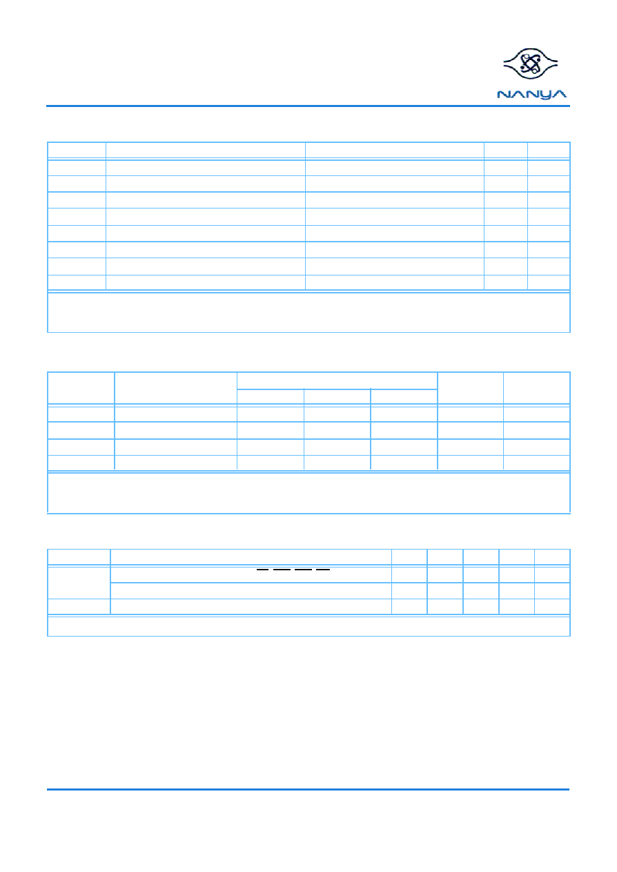
NT5SV32M4CT
NT5SV16M8CT
NT5SV8M16CT
128Mb Synchronous DRAM
REV 1.0
May, 2001
34
©
NANYA TECHNOLOGY CORP
. All rights reserved.
NANYA TECHNOLOGY CORP. reserves the right to change Products and Specifications without notice.
Absolute Maximum Ratings
Symbol
Parameter
Rating
Units
Notes
V
DD
Power Supply Voltage
-0.3 to +4.6
V
1
V
DDQ
Power Supply Voltage for Output
-0.3 to +4.6
V
1
V
IN
Input Voltage
-0.3 to V
DD
+0.3
V
1
V
OUT
Output Voltage
-0.3 to V
DD
+0.3
V
1
T
A
Operating Temperature (ambient)
0 to +70
∞
C
1
T
STG
Storage Temperature
-55 to +125
∞
C
1
P
D
Power Dissipation
1.0
W
1
I
OUT
Short Circuit Output Current
50
mA
1
1. Stresses greater than those listed under "Absolute Maximum Ratings" may cause permanent damage to the device. This is a stress rating
only and functional operation of the device at these or any other conditions above those indicated in the operational sections of this spec-
ification is not implied. Exposure to absolute maximum rating conditions for extended periods may affect reliability.
Recommended DC Operating Conditions
(T
A
=
0
∞
C to 70
∞
C)
Symbol
Parameter
Rating
Units
Notes
Min.
Typ.
Max.
V
DD
Supply Voltage
3.0
3.3
3.6
V
1
V
DDQ
Supply Voltage for Output
3.0
3.3
3.6
V
1
V
IH
Input High Voltage
2.0
--
V
DD
+ 0.3
V
1, 2
V
IL
Input Low Voltage
-0.3
--
0.8
V
1, 3
1. All voltages referenced to V
SS
and V
SSQ
.
2. V
IH
(max) = V
DD
+ 1.2V for pulse width
5ns .
3. V
IL
(min) = V
SS
- 1.2V for pulse width
5ns .
Capacitance
(T
A
= 25
∞
C, f = 1MHz, V
DD
= 3.3V
±
0.3V)
Symbol
Parameter
Min.
Typ
Max.
Units
Notes
C
I
Input Capacitance (A0-A11, BS0, BS1, CS , RAS , CAS, WE , CKE, DQM)
2.5
3.0
3.8
pF
Input Capacitance (CK)
2.5
2.8
3.5
pF
C
O
Output Capacitance (DQ0 - DQ15)
4.0
4.5
6.5
pF
1.
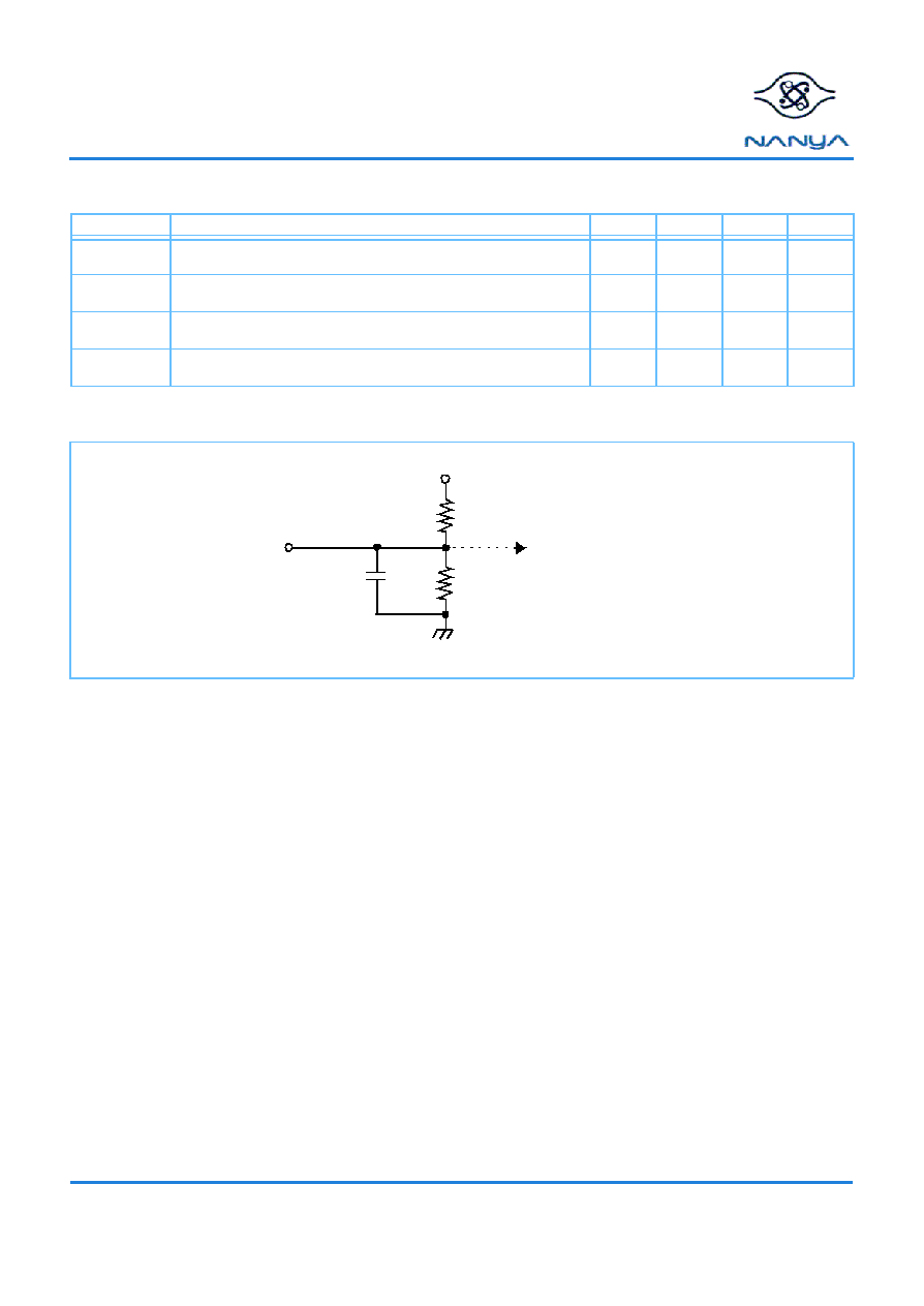
NT5SV32M4CT
NT5SV16M8CT
NT5SV8M16CT
128Mb Synchronous DRAM
REV 1.0
May, 2001
35
©
NANYA TECHNOLOGY CORP
. All rights reserved.
NANYA TECHNOLOGY CORP. reserves the right to change Products and Specifications without notice.
DC Electrical Characteristics
(T
A
= 0 to +70
∞
C, V
DD
= 3.3V
±
0.3V)
Symbol
Parameter
Min.
Max.
Units
Notes
I
I(L)
Input Leakage Current, any input
(0.0V
V
IN
V
DD
), All Other Pins Not Under Test = 0V
-1
+1
µ
A
I
O(L)
Output Leakage Current
(D
OUT
is disabled, 0.0V
V
OUT
V
DDQ
)
-1
+1
µ
A
V
OH
Output Level (LVTTL)
Output "H" Level Voltage (
IOUT
= -2.0mA)
2.4
--
V
V
OL
Output Level (LVTTL)
Output "L" Level Voltage (I
OUT
= +2.0mA)
--
0.4
V
DC Output Load Circuit
Output
1200
50pF
3.3 V
870
V
O H
(DC) = 2.4V, I
O H
= -2mA
V
OL
(DC) = 0.4V, I
OL
= 2mA
NT5SV32M4CT
NT5SV16M8CT
NT5SV8M16CT
128Mb Synchronous DRAM
REV 1.0
May, 2001
36
©
NANYA TECHNOLOGY CORP
. All rights reserved.
NANYA TECHNOLOGY CORP. reserves the right to change Products and Specifications without notice.
Operating, Standby, and Refresh Currents
(T
A
= 0 to +70
∞
C, V
DD
= 3.3V
±
0.3V)
Parameter
Symbol
Test Condition
Speed
Units
Notes
-7K
-75B
-8B
Operating Current
I
CC1
1 bank operation
t
RC
= t
RC
(min), t
C K
= min
Active-Precharge command cycling with-
out burst operation
90
85
80
mA
1, 2, 3
Precharge Standby Current in
Power Down Mode
I
CC2P
CKE
V
IL
(max), t
CK
= min,
CS = V
IH
(min)
2
2
2
mA
1
I
CC2PS
CKE
V
IL
(max), t
CK
= Infinity,
CS = V
IH
(min)
2
2
2
mA
1
Precharge Standby Current in Non-
Power Down Mode
I
CC2N
CKE
V
I H
(min), t
CK
= min,
CS = V
IH
(min)
50
45
35
mA
1, 5
I
CC2NS
CKE
V
I H
(min), t
CK
= Infinity,
9
9
9
mA
1, 7
No Operating Current
(Active state: 4 bank)
I
CC3N
CKE
V
I H
(min), t
CK
= min,
CS = V
IH
(min)
60
50
40
mA
1, 5
I
CC3P
CKE
V
IL
(max), t
CK
= min,
9
9
9
mA
1, 6
Operating Current (Burst Mode)
I
CC4
t
C K
= min,
Read/ Write command cycling,
Multiple banks active, gapless data, BL =
4
135
120
90
mA
1, 3, 4
Auto (CBR) Refresh Current
I
CC5
t
C K
= min, t
RC
= t
RC
(min)
CBR command cycling
190
190
170
mA
1
Self Refresh Current
I
CC6
CKE
0.2V
2
2
2
mA
1
1. Currents given are valid for a single device.
2. These parameters depend on the cycle rate and are measured with the cycle determined by the minimum value of t
C K
and t
RC
. Input sig-
nals are changed up to three times during t
RC
(min).
3. The specified values are obtained with the output open.
4. Input signals are changed once during t
C K
(min).
5. Input signals are changed once during three clock cycles.
6. Active Standby Current will be higher if Clock Suspend is entered during a burst read cycle (add 1mA per DQ).
7. Input signals are stable.
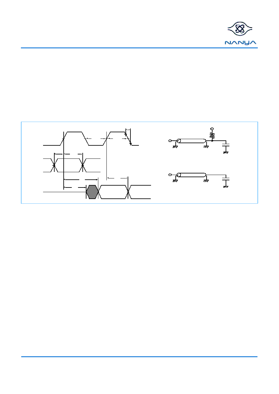
NT5SV32M4CT
NT5SV16M8CT
NT5SV8M16CT
128Mb Synchronous DRAM
REV 1.0
May, 2001
37
©
NANYA TECHNOLOGY CORP
. All rights reserved.
NANYA TECHNOLOGY CORP. reserves the right to change Products and Specifications without notice.
AC Characteristics
(T
A
= 0 to +70
∞
C, V
DD
= 3.3V
±
0.3V)
1. An initial pause of 200
µ
s, with DQM and CKE held high, is required after power-up. A Precharge All Banks command must
be given followed by a minimum of two Auto (CBR) Refresh cycles before or after the Mode Register Set operation.
2. The Transition time is measured between V
IH
and V
IL
(or between V
IL
and V
IH
)
3. In addition to meeting the transition rate specification, the clock and CKE must transit between V
IH
and V
IL
(or between V
IL
and V
IH
) in a monotonic manner.
4. Load Circuit A: AC timing tests have V
IL
= 0.4 V and V
IH
= 2.4 V with the timing referenced to the 1.40V crossover point
5. Load Circuit A: AC measurements assume t
T
= 1.0ns.
6. Load Circuit B: AC timing tests have V
IL
= 0.8 V and V
IH
= 2.0 V with the timing referenced to the 1.40V crossover point
7. Load Circuit B: AC measurements assume t
T
= 1.2ns.
.
AC Characteristics Diagrams
Output
Input
Clock
t
OH
t
SETUP
t
HOLD
t
AC
t
LZ
1.4V
1.4V
1.4V
t
T
Vtt = 1.4V
Output
50
50pF
Z
o
= 50
AC Output Load Circuit (A)
t
CKH
t
CKL
Output
50pF
Z
o
= 50
AC Output Load Circuit (B)
V
IL
V
IH

NT5SV32M4CT
NT5SV16M8CT
NT5SV8M16CT
128Mb Synchronous DRAM
REV 1.0
May, 2001
38
©
NANYA TECHNOLOGY CORP
. All rights reserved.
NANYA TECHNOLOGY CORP. reserves the right to change Products and Specifications without notice.
Clock and Clock Enable Parameters
Symbol
Parameter
-7 K
-75B
-8B
Units
Notes
Min.
Max.
Min.
Max.
Min.
Max.
t
CK3
Clock Cycle Time, CAS Latency = 3
7
1000
7.5
1000
8
1000
ns
t
CK2
Clock Cycle Time, CAS Latency = 2
7.5
1000
10
--
10
1000
ns
t
AC3 (A)
Clock Access Time, CAS Latency = 3
--
--
--
--
--
--
ns
1
t
AC2 (A)
Clock Access Time, CAS Latency = 2
--
--
--
--
--
--
ns
1
t
AC3 (B)
Clock Access Time, CAS Latency = 3
--
5.4
--
5.4
--
6
ns
2
t
AC2 (B)
Clock Access Time, CAS Latency = 2
--
5.4
--
6
--
6
ns
2
t
CKH
Clock High Pulse Width
2.5
--
2.5
--
3
--
ns
t
CKL
Clock Low Pulse Width
2.5
--
2.5
--
3
--
ns
t
CES
Clock Enable Set-up Time
1.5
--
1.5
--
2
--
ns
t
CEH
Clock Enable Hold Time
0.8
--
0.8
--
1
--
ns
t
SB
Power down mode Entry Time
0
7.5
0
7.5
0
10
ns
t
T
Transition Time (Rise and Fall)
0.5
10
0.5
10
0.5
10
ns
1. Access time is measured at 1.4V. See AC Characteristics: notes 1, 2, 3, 4, 5 and load circuit A.
2. Access time is measured at 1.4V. See AC Characteristics: notes 1, 2, 3, 6, 7 and load circuit B.
Common Parameters
Symbol
Parameter
-7K
-75B
-8B
Units
Notes
Min.
Max.
Min.
Max.
Min.
Max.
t
CS
Command Setup Time
1.5
--
1.5
--
2
--
ns
t
CH
Command Hold Time
0.8
--
0.8
--
1
--
ns
t
AS
Address and Bank Select Set-up Time
1.5
--
1.5
--
2
--
ns
t
AH
Address and Bank Select Hold Time
0.8
--
0.8
--
1
--
ns
t
RCD
RAS to CAS Delay
15
--
20
--
20
--
ns
1
t
RC
Bank Cycle Time
60
--
67.5
--
70
--
ns
1
t
RAS
Active Command Period
45
100K
45
100K
50
100K
ns
1
t
RP
Precharge Time
15
--
20
--
20
--
ns
1
t
RRD
Bank to Bank Delay Time
15
--
15
--
20
--
ns
1
t
CCD
CAS to CAS Delay Time
1
--
1
--
1
--
CK
1. These parameters account for the number of clock cycle and depend on the operating frequency of the clock, as follows:
the number of clock cycles = specified value of timing / clock period (count fractions as a whole number).
Mode Register Set Cycle
Symbol
Parameter
-7K
-75B
-8B
Units
Min.
Max.
Min.
Max.
Min.
Max.
t
RSC
Mode Register Set Cycle Time
15
--
15
--
20
--
ns

NT5SV32M4CT
NT5SV16M8CT
NT5SV8M16CT
128Mb Synchronous DRAM
REV 1.0
May, 2001
39
©
NANYA TECHNOLOGY CORP
. All rights reserved.
NANYA TECHNOLOGY CORP. reserves the right to change Products and Specifications without notice.
Read Cycle
Symbol
Parameter
-7K
-75B
-8B
Units
Notes
Min.
Max.
Min.
Max.
Min.
Max.
t
OH
Data Out Hold Time
--
--
--
--
2.5
--
ns
1
2.7
--
2.7
--
3
--
ns
2, 4
t
LZ
Data Out to Low Impedance Time
0
--
0
--
0
--
ns
t
HZ3
Data Out to High Impedance Time
3
5.4
3
5.4
3
6
ns
3
t
HZ2
Data Out to High Impedance Time
3
5.4
3
6
3
6
ns
3
t
DQZ
DQM Data Out Disable Latency
2
--
2
--
2
--
CK
1. AC Output Load Circuit A.
2. AC Output Load Circuit B.
3. Referenced to the time at which the output achieves the open circuit condition, not to output voltage levels.
4. Data Out Hold Time with no load must meet 1.8ns (-7K, -75B).
Refresh Cycle
Symbol
Parameter
-7K
-75B
-8B
Units
Notes
Min.
Max.
Min.
Max.
Min.
Max.
t
REF
Refresh Period
--
64
--
64
--
64
ms
t
SREX
Self Refresh Exit Time
10
--
10
--
10
--
ns
t
RFC
Bank Cycle Time (Auto Refresh)
67.5
67.5
70
ns
1
1. These parameters account for the number of clock cycles and depend on the operating frequency of the clock . as follows; the number of
clock cycles = specified value of timing/clock period (count fractions as a whole number).
Write Cycle
Symbol
Parameter
-7K
-75B
-8B
Units
Min.
Max.
Min.
Max.
Min.
Max.
t
DS
Data In Set-up Time
1.5
--
1.5
--
2
--
ns
t
DH
Data In Hold Time
0.8
--
0.8
--
1
--
ns
t
DPL
Data input to Precharge
15
--
15
--
20
--
ns
t
DAL3
Data In to Active Delay
CAS Latency = 3
5
--
5
--
5
--
CK
t
DAL2
Data In to Active Delay
CAS Latency = 2
5
--
5
--
5
--
CK
t
DQW
DQM Write Mask Latency
0
--
0
--
0
--
CK

NT5SV32M4CT
NT5SV16M8CT
NT5SV8M16CT
128Mb Synchronous DRAM
REV 1.0
May, 2001
40
©
NANYA TECHNOLOGY CORP
. All rights reserved.
NANYA TECHNOLOGY CORP. reserves the right to change Products and Specifications without notice.
Clock Frequency and Latency
Symbol
Parameter
-7 K
-75B
-8B
Units
f
CK
Clock Frequency
143
133
133
100
125
100
MHz
t
CK
Clock Cycle Time
7
7.5
7.5
10
8
10
ns
t
AA
CAS Latency
3
2
3
3
3
2
CK
t
RP
Precharge Time
3
2
3
2
3
2
CK
t
RCD
RAS to CAS Delay
3
2
3
2
3
2
CK
t
R C
Bank Cycle Time
9
8
9
7
9
7
CK
t
RFC
Bank Cycle Time(Auto Refresh)
9
9
9
7
9
7
CK
t
RAS
Minimum Bank Active Time
6
6
6
5
6
5
CK
t
DPL
Data In to Precharge
2
2
2
2
2
2
CK
t
DAL
Data In to Active/Refresh
5
5
5
5
5
5
CK
t
RRD
Bank to Bank Delay Time
2
2
2
2
2
2
CK
t
CCD
CAS to CAS Delay Time
1
1
1
1
1
1
CK
t
WL
Write Latency
0
0
0
0
0
0
CK
t
DQW
DQM Write Mask Latency
0
0
0
0
0
0
CK
t
DQZ
DQM Data Disable Latency
2
2
2
2
2
2
CK
t
CSL
Clock Suspend Latency
1
1
1
1
1
1
CK

NT5SV32M4CT
NT5SV16M8CT
NT5SV8M16CT
128Mb Synchronous DRAM
REV 1.0
May, 2001
41
©
NANYA TECHNOLOGY CORP
. All rights reserved.
NANYA TECHNOLOGY CORP. reserves the right to change Products and Specifications without notice.
Timing Diagrams
Page
AC Parameters for Write Timing................................................................................................................................. 42
AC Parameters for Read Timing (3/3/3), BL=4........................................................................................................... 43
AC Parameters for Read Timing (2/2/2), BL=2........................................................................................................... 44
AC Parameters for Read Timing (3/2/2), BL=2........................................................................................................... 45
AC Parameters for Read Timing (3/3/3), BL=2........................................................................................................... 46
Mode Register Set...................................................................................................................................................... 47
Power on Sequence and Auto Refresh (CBR)............................................................................................................ 48
Clock Suspension / DQM During Burst Read ............................................................................................................ 49
Clock Suspension / DQM During Burst Write ............................................................................................................ 50
Power Down Mode and Clock Suspend ..................................................................................................................... 51
Auto Refresh (CBR) .................................................................................................................................................... 52
Self Refresh (Entry and Exit) ...................................................................................................................................... 53
Random Row Read (Interleaving Banks) with Precharge, BL=8................................................................................ 54
Random Row Read (Interleaving Banks) with Auto-precharge, BL=8........................................................................ 55
Random Row Write (Interleaving Banks) with Auto-Precharge, BL=8........................................................................ 56
Random Row Write (Interleaving Banks) with Precharge, BL=8 ................................................................................ 57
Read/Write Cycle
............................................................................................................................................... 58
Interleaved Column Read Cycle ................................................................................................................................. 59
Auto Precharge after a Read Burst, BL=4 .................................................................................................................. 60
Auto Precharge after a Write Burst, BL=4 .................................................................................................................. 61
Burst Read and Single Write Operation ...................................................................................................................... 62
CS Function (Only CS signal needs to be asserted at minimum rate)........................................................................ 63

NT5SV32M4CT
NT5SV16M8CT
NT5SV8M16CT
128Mb Synchronous DRAM
REV 1.0
May, 2001
42
©
NANYA TECHNOLOGY CORP
. All rights reserved.
NANYA TECHNOLOGY CORP. reserves the right to change Products and Specifications without notice.
AC Parameters for Write Timing
\
C
K
C
K
E
C
S
D
Q
R
A
S
C
A
S
W
E
*
B
S
1
D
Q
M
T
2
T
3
T
4
T
0
T
1
T
6
T
7
T
8
T
9
T
5
T
1
1
T
1
2
T
1
3
T
1
4
T
1
0
T
1
6
T
1
7
T
1
8
T
1
9
T
1
5
T
2
2
T
2
0
T
2
1
H
i
-
Z
A
1
0
A
0
-
A
9
,
t
C
E
S
t
C
S
t
C
H
t
A
S
t
R
C
D
t
D
A
L
t
D
S
A
c
t
i
v
a
t
e
C
o
m
m
a
n
d
B
a
n
k
0
W
r
i
t
e
w
i
t
h
A
u
t
o
P
r
e
c
h
a
r
g
e
C
o
m
m
a
n
d
B
a
n
k
0
A
c
t
i
v
a
t
e
C
o
m
m
a
n
d
B
a
n
k
1
W
r
i
t
e
w
i
t
h
A
u
t
o
P
r
e
c
h
a
r
g
e
C
o
m
m
a
n
d
B
a
n
k
1
A
c
t
i
v
a
t
e
C
o
m
m
a
n
d
B
a
n
k
0
W
r
i
t
e
C
o
m
m
a
n
d
B
a
n
k
0
P
r
e
c
h
a
r
g
e
C
o
m
m
a
n
d
B
a
n
k
0
A
c
t
i
v
a
t
e
C
o
m
m
a
n
d
B
a
n
k
0
t
D
H
A
x
0
A
x
3
A
x
2
A
x
1
B
x
0
B
x
3
B
x
2
B
x
1
A
y
0
A
y
3
A
y
2
A
y
1
t
C
K
2
t
C
K
H
t
C
K
L
A
c
t
i
v
a
t
e
C
o
m
m
a
n
d
B
a
n
k
1
R
A
y
C
B
x
C
A
y
R
A
y
R
B
x
R
B
x
C
A
x
R
B
y
R
B
y
R
A
z
R
A
z
R
A
x
R
A
x
t
A
H
*
B
S
0
=
"
L
"
B
a
n
k
2
,
3
=
I
d
l
e
t
R
C
t
C
E
H
t
D
P
L
t
R
P
t
R
R
D
t
D
P
L
a
n
d
t
D
A
L
d
e
p
e
n
d
o
n
c
l
o
c
k
c
y
c
l
e
t
i
m
e
a
n
d
(
B
u
r
s
t
l
e
n
g
t
h
=
4
,
C
A
S
l
a
t
e
n
c
y
=
2
)
s
p
e
e
d
s
o
r
t
.
S
e
e
t
h
e
C
l
o
c
k
F
r
e
q
u
e
n
c
y
a
n
d
L
a
t
e
n
c
y
T
a
b
l
e
.
A
1
1

NT5SV32M4CT
NT5SV16M8CT
NT5SV8M16CT
128Mb Synchronous DRAM
REV 1.0
May, 2001
43
©
NANYA TECHNOLOGY CORP
. All rights reserved.
NANYA TECHNOLOGY CORP. reserves the right to change Products and Specifications without notice.
AC Parameters for Read Timing (3/3/3)
\
C
K
C
K
E
C
S
D
Q
R
A
S
C
A
S
W
E
*
B
S
1
D
Q
M
T
2
T
3
T
4
T
0
T
1
T
6
T
7
T
8
T
9
T
5
T
1
1
T
1
2
T
1
3
T
1
0
H
i
-
Z
A
1
0
A
0
-
A
9
,
t
R
C
D
t
R
A
S
A
c
t
i
v
a
t
e
C
o
m
m
a
n
d
B
a
n
k
0
A
c
t
i
v
a
t
e
C
o
m
m
a
n
d
B
a
n
k
1
A
c
t
i
v
a
t
e
C
o
m
m
a
n
d
B
a
n
k
0
t
C
K
3
R
e
a
d
w
i
t
h
A
u
t
o
P
r
e
c
h
a
r
g
e
C
o
m
m
a
n
d
B
a
n
k
1
t
R
C
t
A
C
3
t
O
H
B
x
0
B
x
1
C
B
x
R
A
y
R
B
x
R
B
x
R
A
y
C
A
x
R
A
x
R
A
x
*
B
S
0
=
"
L
"
R
e
a
d
w
i
t
h
A
u
t
o
P
r
e
c
h
a
r
g
e
C
o
m
m
a
n
d
B
a
n
k
0
B
e
g
i
n
A
u
t
o
P
r
e
c
h
a
r
g
e
B
a
n
k
0
B
a
n
k
2
,
3
=
I
d
l
e
t
R
P
B
x
2
B
e
g
i
n
A
u
t
o
P
r
e
c
h
a
r
g
e
B
a
n
k
1
t
R
R
D
A
x
3
A
x
2
A
x
1
A
x
0
(
B
u
r
s
t
l
e
n
g
t
h
=
4
,
C
A
S
l
a
t
e
n
c
y
=
3
;
t
R
C
D
,
t
R
P
=
3
)
A
1
1

NT5SV32M4CT
NT5SV16M8CT
NT5SV8M16CT
128Mb Synchronous DRAM
REV 1.0
May, 2001
44
©
NANYA TECHNOLOGY CORP
. All rights reserved.
NANYA TECHNOLOGY CORP. reserves the right to change Products and Specifications without notice.
AC Parameters for Read Timing (2/2/2)
\
C
K
C
K
E
C
S
D
Q
R
A
S
C
A
S
W
E
*
B
S
1
D
Q
M
T
2
T
3
T
4
T
0
T
1
T
6
T
7
T
8
T
9
T
5
T
1
1
T
1
2
T
1
3
T
1
0
H
i
-
Z
A
1
0
t
C
S
t
C
H
t
C
E
H
t
A
S
t
A
H
t
R
R
D
t
R
C
D
t
R
A
S
(
m
i
n
)
t
L
Z
A
c
t
i
v
a
t
e
C
o
m
m
a
n
d
B
a
n
k
0
A
c
t
i
v
a
t
e
C
o
m
m
a
n
d
B
a
n
k
1
A
c
t
i
v
a
t
e
C
o
m
m
a
n
d
B
a
n
k
0
t
C
E
S
t
C
K
2
R
e
a
d
w
i
t
h
A
u
t
o
P
r
e
c
h
a
r
g
e
C
o
m
m
a
n
d
B
a
n
k
1
t
R
C
t
R
P
t
A
C
2
t
O
H
t
H
Z
t
C
K
H
B
x
0
B
e
g
i
n
A
u
t
o
P
r
e
c
h
a
r
g
e
B
a
n
k
1
B
x
1
t
H
Z
C
B
x
R
A
y
R
B
x
R
B
x
R
A
y
C
A
x
R
A
x
R
A
x
t
C
K
L
A
x
0
A
x
1
*
B
S
0
=
"
L
"
R
e
a
d
w
i
t
h
A
u
t
o
P
r
e
c
h
a
r
g
e
C
o
m
m
a
n
d
B
a
n
k
0
B
e
g
i
n
A
u
t
o
P
r
e
c
h
a
r
g
e
B
a
n
k
0
B
a
n
k
2
,
3
=
I
d
l
e
t
R
P
N
o
t
e
:
M
u
s
t
s
a
t
i
s
f
y
t
R
A
S
(
m
i
n
)
F
o
r
-
2
6
0
:
e
x
t
e
n
d
t
R
C
D
1
c
l
o
c
k
(
B
u
r
s
t
l
e
n
g
t
h
=
2
,
C
A
S
l
a
t
e
n
c
y
=
2
;
t
R
C
D
,
t
R
P
=
2
)
A
0
-
A
9
,
A
1
1
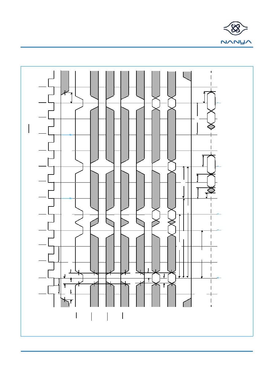
NT5SV32M4CT
NT5SV16M8CT
NT5SV8M16CT
128Mb Synchronous DRAM
REV 1.0
May, 2001
45
©
NANYA TECHNOLOGY CORP
. All rights reserved.
NANYA TECHNOLOGY CORP. reserves the right to change Products and Specifications without notice.
AC Parameters for Read Timing (3/2/2)
\
C
K
C
K
E
C
S
D
Q
R
A
S
C
A
S
W
E
*
B
S
1
D
Q
M
T
2
T
3
T
4
T
0
T
1
T
6
T
7
T
8
T
9
T
5
T
1
1
T
1
2
T
1
3
T
1
0
H
i
-
Z
A
1
0
t
C
S
t
C
H
t
C
E
H
t
A
S
t
A
H
t
R
C
D
t
L
Z
A
c
t
i
v
a
t
e
C
o
m
m
a
n
d
B
a
n
k
0
A
c
t
i
v
a
t
e
C
o
m
m
a
n
d
B
a
n
k
1
A
c
t
i
v
a
t
e
C
o
m
m
a
n
d
B
a
n
k
0
t
C
K
3
R
e
a
d
w
i
t
h
A
u
t
o
P
r
e
c
h
a
r
g
e
C
o
m
m
a
n
d
B
a
n
k
1
t
R
P
t
A
C
3
t
O
H
t
H
Z
t
C
K
H
B
x
0
B
e
g
i
n
A
u
t
o
P
r
e
c
h
a
r
g
e
B
a
n
k
1
B
x
1
t
H
Z
C
B
x
R
A
y
R
B
x
R
B
x
R
A
y
C
A
x
R
A
x
R
A
x
t
C
K
L
A
x
0
A
x
1
*
B
S
0
=
"
L
"
R
e
a
d
w
i
t
h
A
u
t
o
P
r
e
c
h
a
r
g
e
C
o
m
m
a
n
d
B
a
n
k
0
B
e
g
i
n
A
u
t
o
P
r
e
c
h
a
r
g
e
B
a
n
k
0
B
a
n
k
2
,
3
=
I
d
l
e
t
R
P
t
C
E
S
N
o
t
e
:
M
u
s
t
s
a
t
i
s
f
y
t
R
A
S
(
m
i
n
)
.
E
x
t
e
n
d
e
d
t
R
C
D
1
c
l
o
c
k
.
N
o
t
r
e
q
u
i
r
e
d
f
o
r
B
L
4
.
t
R
R
D
t
R
A
S
t
R
C
(
B
u
r
s
t
l
e
n
g
t
h
=
2
,
C
A
S
l
a
t
e
n
c
y
=
3
;
t
R
C
D
,
t
R
P
=
2
)
A
0
-
A
9
,
A
1
1

NT5SV32M4CT
NT5SV16M8CT
NT5SV8M16CT
128Mb Synchronous DRAM
REV 1.0
May, 2001
46
©
NANYA TECHNOLOGY CORP
. All rights reserved.
NANYA TECHNOLOGY CORP. reserves the right to change Products and Specifications without notice.
AC Parameters for Read Timing (3/3/3)
\
C
K
C
K
E
C
S
D
Q
R
A
S
C
A
S
W
E
*
B
S
1
D
Q
M
T
2
T
3
T
4
T
0
T
1
T
6
T
7
T
8
T
9
T
5
T
1
1
T
1
2
T
1
3
T
1
0
H
i
-
Z
A
1
0
A
0
-
A
9
,
t
R
R
D
t
R
C
D
t
R
A
S
(
m
I
n
)
A
c
t
i
v
a
t
e
C
o
m
m
a
n
d
B
a
n
k
0
A
c
t
i
v
a
t
e
C
o
m
m
a
n
d
B
a
n
k
1
A
c
t
i
v
a
t
e
C
o
m
m
a
n
d
B
a
n
k
0
t
C
K
3
R
e
a
d
w
i
t
h
A
u
t
o
P
r
e
c
h
a
r
g
e
C
o
m
m
a
n
d
B
a
n
k
1
t
R
C
t
R
P
t
A
C
3
t
O
H
B
x
0
B
e
g
i
n
A
u
t
o
P
r
e
c
h
a
r
g
e
B
a
n
k
1
B
x
1
C
B
x
R
A
y
R
B
x
R
B
x
R
A
y
C
A
x
R
A
x
R
A
x
R
e
a
d
w
i
t
h
A
u
t
o
P
r
e
c
h
a
r
g
e
C
o
m
m
a
n
d
B
a
n
k
0
B
e
g
i
n
A
u
t
o
P
r
e
c
h
a
r
g
e
B
a
n
k
0
t
R
P
A
x
0
A
x
1
N
o
t
e
:
M
u
s
t
s
a
t
i
s
f
y
t
R
A
S
(
m
i
n
)
.
E
x
t
e
n
d
e
d
t
R
C
D
n
o
t
r
e
q
u
i
r
e
d
f
o
r
B
L
4
.
t
C
E
H
A
1
1
T
1
4
*
B
S
0
=
"
L
"
B
a
n
k
2
,
3
=
I
d
l
e
(
B
u
r
s
t
l
e
n
g
t
h
=
2
,
C
A
S
l
a
t
e
n
c
y
=
3
;
t
R
C
D
,
t
R
P
=
3
)
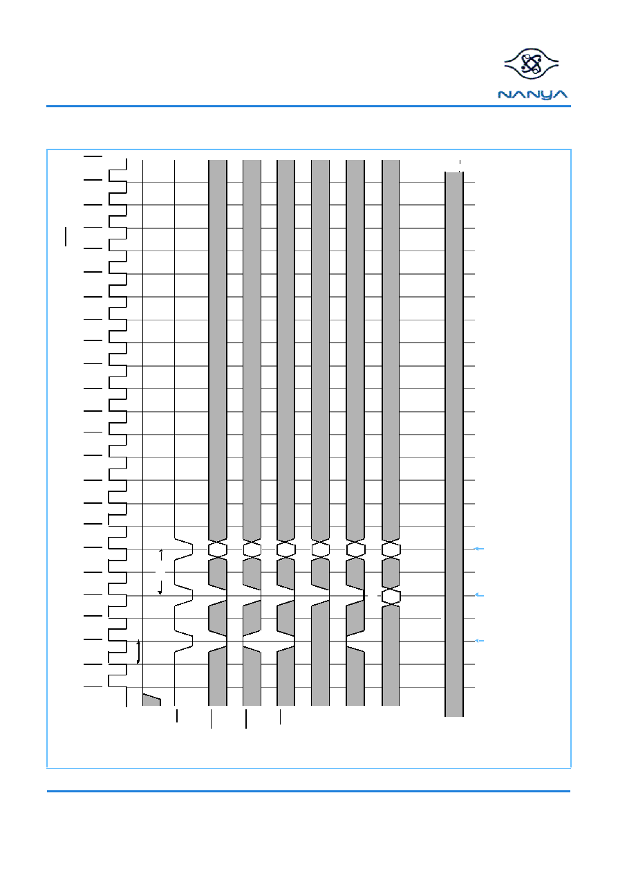
NT5SV32M4CT
NT5SV16M8CT
NT5SV8M16CT
128Mb Synchronous DRAM
REV 1.0
May, 2001
47
©
NANYA TECHNOLOGY CORP
. All rights reserved.
NANYA TECHNOLOGY CORP. reserves the right to change Products and Specifications without notice.
Mode Register Set
\
C
K
C
K
E
C
S
D
Q
R
A
S
C
A
S
W
E
B
S
0
,
B
S
1
D
Q
M
T
2
T
3
T
4
T
0
T
1
T
6
T
7
T
8
T
9
T
5
T
1
1
T
1
2
T
1
3
T
1
4
T
1
0
T
1
6
T
1
7
T
1
8
T
1
9
T
1
5
T
2
2
T
2
0
T
2
1
H
i
-
Z
A
1
0
,
A
1
1
A
0
-
A
9
P
r
e
c
h
a
r
g
e
C
o
m
m
a
n
d
A
l
l
B
a
n
k
s
M
o
d
e
R
e
g
i
s
t
e
r
S
e
t
C
o
m
m
a
n
d
A
n
y
C
o
m
m
a
n
d
A
d
d
r
e
s
s
K
e
y
t
R
P
t
C
K
2
t
R
S
C
(
C
A
S
l
a
t
e
n
c
y
=
2
)

NT5SV32M4CT
NT5SV16M8CT
NT5SV8M16CT
128Mb Synchronous DRAM
REV 1.0
May, 2001
48
©
NANYA TECHNOLOGY CORP
. All rights reserved.
NANYA TECHNOLOGY CORP. reserves the right to change Products and Specifications without notice.
Power-On Sequence and Auto Refresh (CBR)
\
C
K
C
K
E
C
S
D
Q
R
A
S
C
A
S
W
E
B
S
D
Q
M
T
2
T
3
T
4
T
0
T
1
T
6
T
7
T
8
T
9
T
5
T
1
1
T
1
2
T
1
3
T
1
4
T
1
0
T
1
6
T
1
7
T
1
8
T
1
9
T
1
5
T
2
2
T
2
0
T
2
1
H
i
-
Z
A
1
0
A
0
-
A
9
,
P
r
e
c
h
a
r
g
e
C
o
m
m
a
n
d
A
l
l
B
a
n
k
s
t
R
P
M
i
n
i
m
u
m
o
f
8
R
e
f
r
e
s
h
C
y
c
l
e
s
a
r
e
r
e
q
u
i
r
e
d
1
s
t
A
u
t
o
R
e
f
r
e
s
h
C
o
m
m
a
n
d
t
R
C
H
i
g
h
l
e
v
e
l
i
s
r
e
q
u
i
r
e
d
8
t
h
A
u
t
o
R
e
f
r
e
s
h
C
o
m
m
a
n
d
I
n
p
u
t
s
m
u
s
t
b
e
s
t
a
b
l
e
f
o
r
2
0
0
µ
s
t
C
K
A
n
y
C
o
m
m
a
n
d
2
C
l
o
c
k
m
i
n
.
M
o
d
e
R
e
g
i
s
t
e
r
A
d
d
r
e
s
s
K
e
y
S
e
t
C
o
m
m
a
n
d
A
1
1

NT5SV32M4CT
NT5SV16M8CT
NT5SV8M16CT
128Mb Synchronous DRAM
REV 1.0
May, 2001
49
©
NANYA TECHNOLOGY CORP
. All rights reserved.
NANYA TECHNOLOGY CORP. reserves the right to change Products and Specifications without notice.
Clock Suspension / DQM During Burst Read
\
C
K
C
K
E
C
S
D
Q
R
A
S
C
A
S
W
E
D
Q
M
T
2
T
3
T
4
T
0
T
1
T
6
T
7
T
8
T
9
T
5
T
1
1
T
1
2
T
1
3
T
1
4
T
1
0
T
1
6
T
1
7
T
1
8
T
1
9
T
1
5
T
2
2
T
2
0
T
2
1
H
i
-
Z
A
1
0
A
0
-
A
9
,
R
A
x
A
x
0
A
x
1
A
x
2
A
x
3
A
c
t
i
v
a
t
e
C
o
m
m
a
n
d
B
a
n
k
0
C
l
o
c
k
S
u
s
p
e
n
d
2
C
y
c
l
e
s
C
l
o
c
k
S
u
s
p
e
n
d
1
C
y
c
l
e
C
l
o
c
k
S
u
s
p
e
n
d
3
C
y
c
l
e
s
R
A
x
R
e
a
d
C
o
m
m
a
n
d
B
a
n
k
0
C
A
x
t
H
Z
t
C
K
3
*
B
S
1
A
x
4
A
x
6
A
x
7
t
C
E
S
t
C
E
H
*
B
S
0
=
"
L
"
B
a
n
k
2
,
3
=
I
d
l
e
(
B
u
r
s
t
l
e
n
g
t
h
=
8
,
C
A
S
l
a
t
e
n
c
y
=
3
;
t
R
C
D
=
3
)
A
1
1
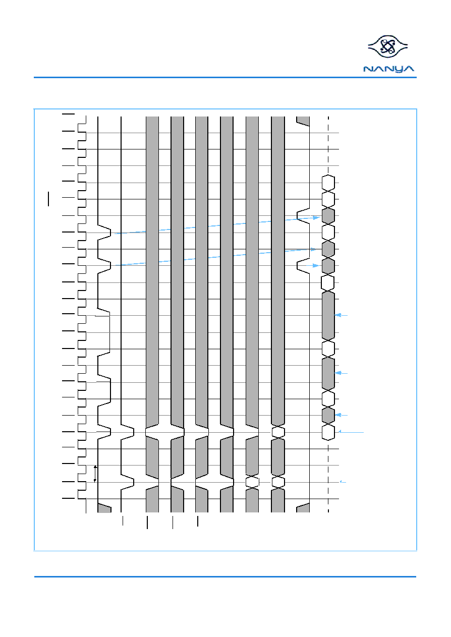
NT5SV32M4CT
NT5SV16M8CT
NT5SV8M16CT
128Mb Synchronous DRAM
REV 1.0
May, 2001
50
©
NANYA TECHNOLOGY CORP
. All rights reserved.
NANYA TECHNOLOGY CORP. reserves the right to change Products and Specifications without notice.
Clock Suspension / DQM During Burst Write
\
C
K
C
K
E
C
S
D
Q
R
A
S
C
A
S
W
E
*
B
S
1
D
Q
M
T
2
T
3
T
4
T
0
T
1
T
6
T
7
T
8
T
9
T
5
T
1
1
T
1
2
T
1
3
T
1
4
T
1
0
T
1
6
T
1
7
T
1
8
T
1
9
T
1
5
T
2
2
T
2
0
T
2
1
H
i
-
Z
A
1
0
A
0
-
A
9
,
R
A
x
A
c
t
i
v
a
t
e
C
o
m
m
a
n
d
B
a
n
k
0
R
A
x
C
A
x
D
A
x
0
C
l
o
c
k
S
u
s
p
e
n
d
1
C
y
c
l
e
D
A
x
1
D
A
x
2
C
l
o
c
k
S
u
s
p
e
n
d
2
C
y
c
l
e
s
C
l
o
c
k
S
u
s
p
e
n
d
3
C
y
c
l
e
s
W
r
i
t
e
C
o
m
m
a
n
d
B
a
n
k
0
t
C
K
3
D
A
x
5
D
A
x
6
D
A
x
7
D
A
x
3
*
B
S
0
=
"
L
"
B
a
n
k
2
,
3
=
I
d
l
e
(
B
u
r
s
t
l
e
n
g
t
h
=
8
,
C
A
S
l
a
t
e
n
c
y
=
3
;
t
R
C
D
=
3
)
A
1
1
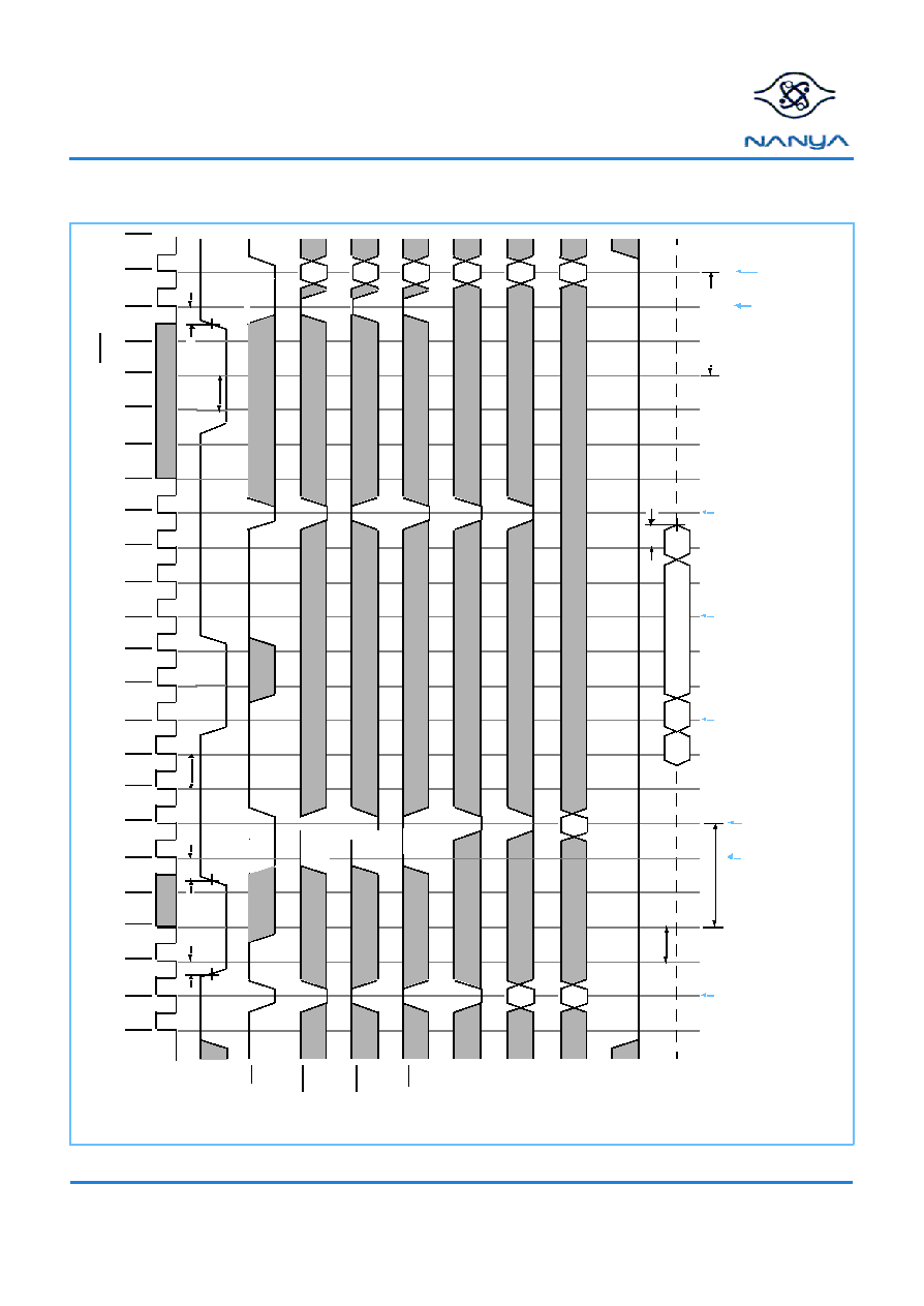
NT5SV32M4CT
NT5SV16M8CT
NT5SV8M16CT
128Mb Synchronous DRAM
REV 1.0
May, 2001
51
©
NANYA TECHNOLOGY CORP
. All rights reserved.
NANYA TECHNOLOGY CORP. reserves the right to change Products and Specifications without notice.
Power Down Mode and Clock Suspend
\
C
K
C
K
E
C
S
D
Q
R
A
S
C
A
S
W
E
*
B
S
1
D
Q
M
T
2
T
3
T
4
T
0
T
1
T
6
T
7
T
8
T
9
T
5
T
1
1
T
1
2
T
1
3
T
1
4
T
1
0
T
1
6
T
1
7
T
1
8
T
1
9
T
1
5
T
2
2
T
2
0
T
2
1
H
i
-
Z
A
1
0
A
0
-
A
9
,
t
C
E
S
t
C
E
S
V
A
L
I
D
C
A
x
R
A
x
R
A
x
A
x
2
A
x
0
A
x
1
A
x
3
A
c
t
i
v
a
t
e
C
o
m
m
a
n
d
B
a
n
k
0
N
O
P
R
e
a
d
C
o
m
m
a
n
d
B
a
n
k
0
A
C
T
I
V
E
S
T
A
N
D
B
Y
C
l
o
c
k
S
u
s
p
e
n
s
i
o
n
S
t
a
r
t
C
l
o
c
k
S
u
s
p
e
n
s
i
o
n
E
n
d
P
r
e
c
h
a
r
g
e
C
o
m
m
a
n
d
B
a
n
k
0
P
R
E
C
H
A
R
G
E
S
T
A
N
D
B
Y
t
H
Z
A
n
y
C
o
m
m
a
n
d
t
C
K
2
t
C
E
S
t
S
B
N
O
P
*
B
S
0
=
"
L
"
B
a
n
k
2
,
3
=
I
d
l
e
t
S
B
(
B
u
r
s
t
l
e
n
g
t
h
=
4
,
C
A
S
l
a
t
e
n
c
y
=
2
)
A
1
1

NT5SV32M4CT
NT5SV16M8CT
NT5SV8M16CT
128Mb Synchronous DRAM
REV 1.0
May, 2001
52
©
NANYA TECHNOLOGY CORP
. All rights reserved.
NANYA TECHNOLOGY CORP. reserves the right to change Products and Specifications without notice.
Auto Refresh (CBR)
\
C
K
C
K
E
C
S
D
Q
R
A
S
C
A
S
W
E
B
S
D
Q
M
T
2
T
3
T
4
T
0
T
1
T
6
T
7
T
8
T
9
T
5
T
1
1
T
1
2
T
1
3
T
1
4
T
1
0
T
1
6
T
1
7
T
1
8
T
1
9
T
1
5
T
2
2
T
2
0
T
2
1
H
i
-
Z
A
1
0
A
0
-
A
9
,
P
r
e
c
h
a
r
g
e
C
o
m
m
a
n
d
A
u
t
o
R
e
f
r
e
s
h
C
o
m
m
a
n
d
A
u
t
o
R
e
f
r
e
s
h
C
o
m
m
a
n
d
t
R
F
C
t
R
P
t
R
F
C
t
C
K
2
A
l
l
B
a
n
k
s
(
C
A
S
l
a
t
e
n
c
y
=
2
)
A
1
1

NT5SV32M4CT
NT5SV16M8CT
NT5SV8M16CT
128Mb Synchronous DRAM
REV 1.0
May, 2001
53
©
NANYA TECHNOLOGY CORP
. All rights reserved.
NANYA TECHNOLOGY CORP. reserves the right to change Products and Specifications without notice.
Self Refresh (Entry and Exit)
\
C
K
C
K
E
C
S
D
Q
R
A
S
C
A
S
W
E
B
S
D
Q
M
T
2
T
3
T
4
T
0
T
1
H
i
-
Z
A
1
0
A
l
l
B
a
n
k
s
m
u
s
t
b
e
i
d
l
e
S
e
l
f
R
e
f
r
e
s
h
E
n
t
r
y
A
0
-
A
9
,
T
m
T
m
+
2
T
m
+
3
T
m
+
4
T
m
+
5
T
m
+
1
T
m
+
7
T
m
+
8
T
m
+
9
T
m
+
1
0
T
m
+
6
T
m
+
1
3
T
m
+
1
1
T
m
+
1
2
T
m
+
1
5
T
m
+
1
4
t
C
E
S
t
S
B
A
n
y
C
o
m
m
a
n
d
t
C
E
S
t
R
C
t
S
R
E
X
S
e
l
f
R
e
f
r
e
s
h
E
x
i
t
P
o
w
e
r
D
o
w
n
E
n
t
r
y
P
o
w
e
r
D
o
w
n
E
x
i
t
(
N
o
t
e
:
T
h
e
C
K
s
i
g
n
a
l
m
u
s
t
b
e
r
e
e
s
t
a
b
l
i
s
h
e
d
p
r
i
o
r
t
o
C
K
E
r
e
t
u
r
n
i
n
g
h
i
g
h
.
)
A
1
1
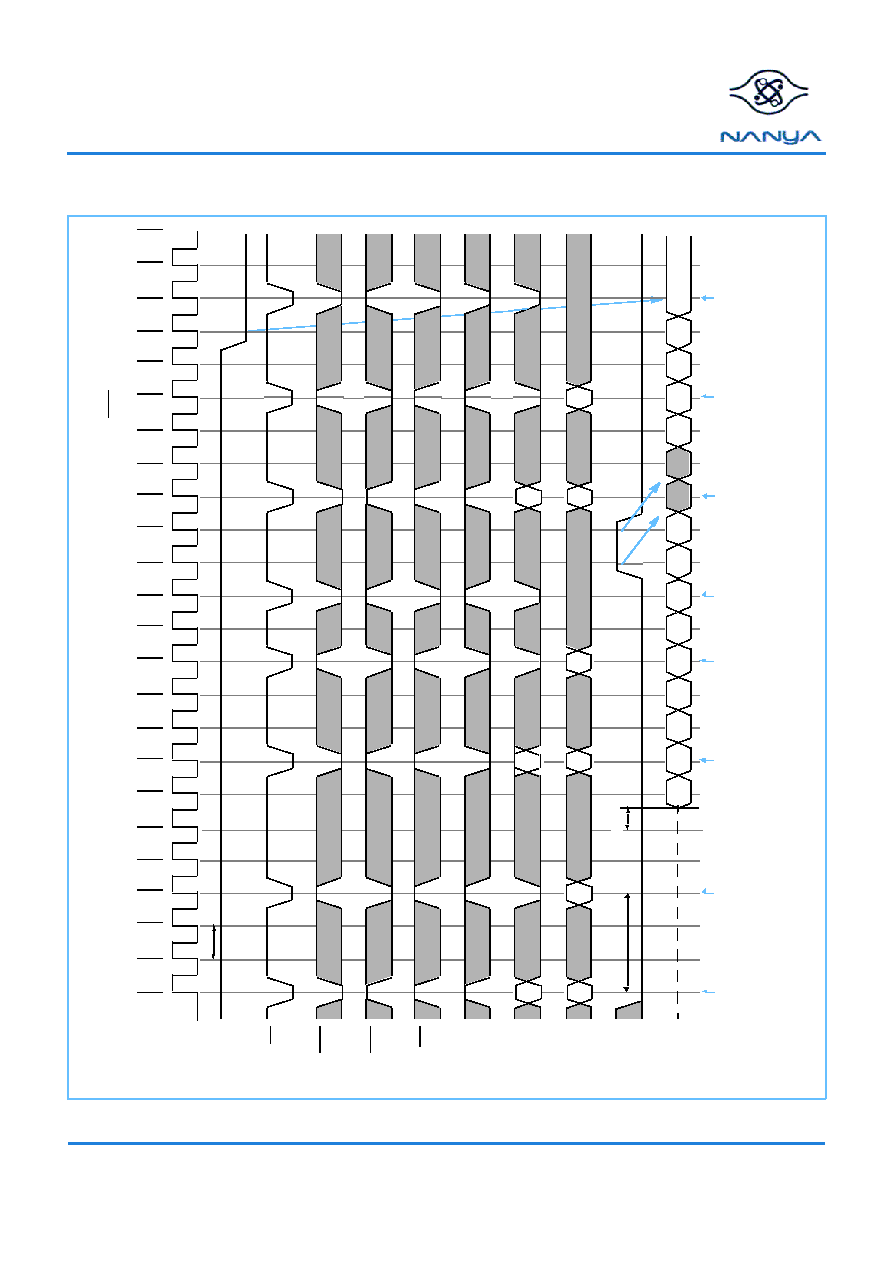
NT5SV32M4CT
NT5SV16M8CT
NT5SV8M16CT
128Mb Synchronous DRAM
REV 1.0
May, 2001
54
©
NANYA TECHNOLOGY CORP
. All rights reserved.
NANYA TECHNOLOGY CORP. reserves the right to change Products and Specifications without notice.
Random Row Read (Interleaving Banks) with Precharge
\
C
K
C
K
E
C
S
D
Q
R
A
S
C
A
S
W
E
*
B
S
1
D
Q
M
T
2
T
3
T
4
T
0
T
1
T
6
T
7
T
8
T
9
T
5
T
1
1
T
1
2
T
1
3
T
1
4
T
1
0
T
1
6
T
1
7
T
1
8
T
1
9
T
1
5
T
2
2
T
2
0
T
2
1
H
i
-
Z
A
1
0
A
0
-
A
9
,
C
B
y
R
e
a
d
C
o
m
m
a
n
d
B
a
n
k
1
B
y
0
t
C
K
3
H
i
g
h
t
A
C
3
A
c
t
i
v
a
t
e
C
o
m
m
a
n
d
B
a
n
k
1
R
B
x
R
B
x
A
c
t
i
v
a
t
e
C
o
m
m
a
n
d
B
a
n
k
0
R
A
x
R
A
x
C
B
x
R
e
a
d
C
o
m
m
a
n
d
B
a
n
k
1
A
c
t
i
v
a
t
e
C
o
m
m
a
n
d
B
a
n
k
1
R
B
y
R
B
y
t
R
C
D
P
r
e
c
h
a
r
g
e
C
o
m
m
a
n
d
B
a
n
k
1
C
A
x
R
e
a
d
C
o
m
m
a
n
d
B
a
n
k
0
B
x
0
B
x
1
B
x
2
B
x
3
B
x
4
B
x
5
B
x
6
A
x
0
A
x
1
A
x
4
A
x
5
A
x
6
A
x
7
P
r
e
c
h
a
r
g
e
C
o
m
m
a
n
d
B
a
n
k
0
*
B
S
0
=
"
L
"
B
a
n
k
2
,
3
=
I
d
l
e
(
B
u
r
s
t
l
e
n
g
t
h
=
8
,
C
A
S
l
a
t
e
n
c
y
=
3
;
t
R
C
D
,
t
R
P
=
3
)
A
1
1
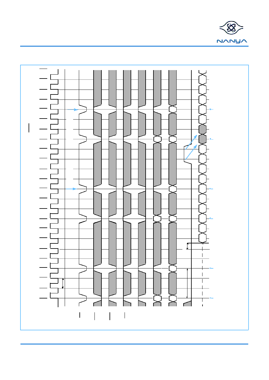
NT5SV32M4CT
NT5SV16M8CT
NT5SV8M16CT
128Mb Synchronous DRAM
REV 1.0
May, 2001
55
©
NANYA TECHNOLOGY CORP
. All rights reserved.
NANYA TECHNOLOGY CORP. reserves the right to change Products and Specifications without notice.
Random Row Read (Interleaving Banks) with Auto-Precharge
\
C
K
C
K
E
C
S
D
Q
R
A
S
C
A
S
W
E
*
B
S
1
D
Q
M
T
2
T
3
T
4
T
0
T
1
T
6
T
7
T
8
T
9
T
5
T
1
1
T
1
2
T
1
3
T
1
4
T
1
0
T
1
6
T
1
7
T
1
8
T
1
9
T
1
5
T
2
2
T
2
0
T
2
1
H
i
-
Z
A
1
0
A
0
-
A
9
,
C
B
y
B
y
0
t
C
K
3
H
i
g
h
t
A
C
3
A
c
t
i
v
a
t
e
C
o
m
m
a
n
d
B
a
n
k
1
R
B
x
R
B
x
A
c
t
i
v
a
t
e
C
o
m
m
a
n
d
B
a
n
k
0
R
A
x
R
A
x
C
B
x
A
c
t
i
v
a
t
e
C
o
m
m
a
n
d
B
a
n
k
1
R
B
y
R
B
y
t
R
C
D
C
A
x
B
x
0
B
x
1
B
x
2
B
x
3
B
x
4
B
x
5
B
x
6
B
x
7
A
x
0
A
x
4
A
x
5
A
x
6
R
e
a
d
w
i
t
h
A
u
t
o
P
r
e
c
h
a
r
g
e
C
o
m
m
a
n
d
B
a
n
k
1
A
x
1
S
t
a
r
t
A
u
t
o
P
r
e
c
h
a
r
g
e
B
a
n
k
1
R
e
a
d
w
i
t
h
A
u
t
o
P
r
e
c
h
a
r
g
e
C
o
m
m
a
n
d
B
a
n
k
0
S
t
a
r
t
A
u
t
o
P
r
e
c
h
a
r
g
e
B
a
n
k
0
R
e
a
d
w
i
t
h
A
u
t
o
P
r
e
c
h
a
r
g
e
C
o
m
m
a
n
d
B
a
n
k
1
*
B
S
0
=
"
L
"
B
a
n
k
2
,
3
=
I
d
l
e
R
A
x
R
A
x
A
x
7
(
B
u
r
s
t
l
e
n
g
t
h
=
8
,
C
A
S
l
a
t
e
n
c
y
=
3
;
t
R
C
D
,
t
R
P
=
3
)
A
1
1

NT5SV32M4CT
NT5SV16M8CT
NT5SV8M16CT
128Mb Synchronous DRAM
REV 1.0
May, 2001
56
©
NANYA TECHNOLOGY CORP
. All rights reserved.
NANYA TECHNOLOGY CORP. reserves the right to change Products and Specifications without notice.
Random Row Write (Interleaving Banks) with Auto-Precharge
\
C
K
C
K
E
C
S
D
Q
R
A
S
C
A
S
W
E
*
B
S
1
D
Q
M
T
2
T
3
T
4
T
0
T
1
T
6
T
7
T
8
T
9
T
5
T
1
1
T
1
2
T
1
3
T
1
4
T
1
0
T
1
6
T
1
7
T
1
8
T
1
9
T
1
5
T
2
2
T
2
0
T
2
1
H
i
-
Z
A
1
0
A
0
-
A
9
,
t
C
K
3
H
i
g
h
D
A
x
0
D
A
x
1
D
A
x
4
D
A
x
7
D
A
x
6
D
A
x
5
D
B
x
0
D
B
x
3
D
B
x
2
D
B
x
1
D
B
x
4
D
B
x
5
D
A
y
2
D
A
y
1
D
A
y
0
C
A
X
A
c
t
i
v
a
t
e
C
o
m
m
a
n
d
B
a
n
k
0
R
A
x
R
A
x
A
c
t
i
v
a
t
e
C
o
m
m
a
n
d
B
a
n
k
1
R
B
x
R
B
x
A
c
t
i
v
a
t
e
C
o
m
m
a
n
d
B
a
n
k
0
R
A
y
R
A
y
C
B
x
C
A
y
t
R
C
D
D
B
x
7
D
B
x
6
W
r
i
t
e
w
i
t
h
A
u
t
o
P
r
e
c
h
a
r
g
e
C
o
m
m
a
n
d
B
a
n
k
0
W
r
i
t
e
w
i
t
h
A
u
t
o
P
r
e
c
h
a
r
g
e
C
o
m
m
a
n
d
B
a
n
k
1
W
r
i
t
e
w
i
t
h
A
u
t
o
P
r
e
c
h
a
r
g
e
C
o
m
m
a
n
d
B
a
n
k
0
*
B
S
0
=
"
L
"
B
a
n
k
2
,
3
=
I
d
l
e
t
D
A
L
t
D
A
L
N
u
m
b
e
r
o
f
c
l
o
c
k
s
d
e
p
e
n
d
s
o
n
c
l
o
c
k
c
y
c
l
e
t
i
m
e
a
n
d
s
p
e
e
d
s
o
r
t
.
S
e
e
t
h
e
C
l
o
c
k
F
r
e
q
u
e
n
c
y
a
n
d
L
a
t
e
n
c
y
t
a
b
l
e
.
B
a
n
k
m
a
y
b
e
r
e
a
c
t
i
v
a
t
e
d
a
t
t
h
e
c
o
m
p
l
e
t
i
o
n
o
f
t
D
A
L
.
(
B
u
r
s
t
l
e
n
g
t
h
=
8
,C
A
S
l
a
t
e
n
c
y
=
3
;
t
R
C
D
,
t
R
P
=
3
)
A
1
1
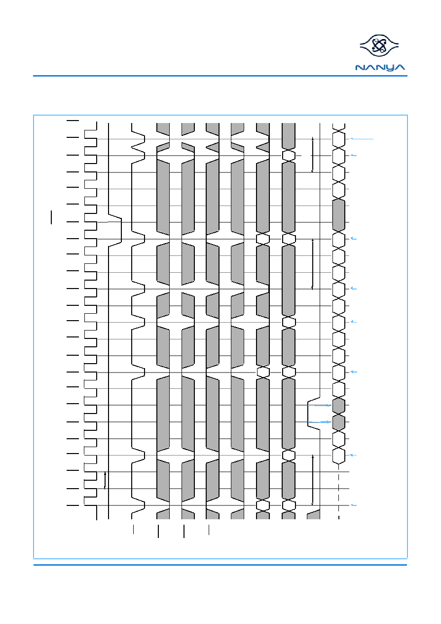
NT5SV32M4CT
NT5SV16M8CT
NT5SV8M16CT
128Mb Synchronous DRAM
REV 1.0
May, 2001
57
©
NANYA TECHNOLOGY CORP
. All rights reserved.
NANYA TECHNOLOGY CORP. reserves the right to change Products and Specifications without notice.
Random Row Write (Interleaving Banks) with Precharge
\
C
K
C
K
E
C
S
D
Q
R
A
S
C
A
S
W
E
*
B
S
1
D
Q
M
T
2
T
3
T
4
T
0
T
1
T
6
T
7
T
8
T
9
T
5
T
1
1
T
1
2
T
1
3
T
1
4
T
1
0
T
1
6
T
1
7
T
1
8
T
1
9
T
1
5
T
2
2
T
2
0
T
2
1
H
i
-
Z
A
1
0
A
0
-
A
9
,
t
C
K
3
H
i
g
h
D
A
x
0
D
A
x
1
D
A
x
4
D
A
x
7
D
A
x
6
D
A
x
5
D
B
x
0
D
B
x
3
D
B
x
2
D
B
x
1
D
B
x
4
D
B
x
5
D
A
y
2
D
A
y
1
D
A
y
0
W
r
i
t
e
C
o
m
m
a
n
d
B
a
n
k
0
C
A
X
A
c
t
i
v
a
t
e
C
o
m
m
a
n
d
B
a
n
k
0
R
A
x
R
A
x
A
c
t
i
v
a
t
e
C
o
m
m
a
n
d
B
a
n
k
1
R
B
x
R
B
x
A
c
t
i
v
a
t
e
C
o
m
m
a
n
d
B
a
n
k
0
R
A
y
R
A
y
C
B
x
W
r
i
t
e
C
o
m
m
a
n
d
B
a
n
k
1
P
r
e
c
h
a
r
g
e
C
o
m
m
a
n
d
B
a
n
k
0
W
r
i
t
e
C
o
m
m
a
n
d
B
a
n
k
0
C
A
y
P
r
e
c
h
a
r
g
e
C
o
m
m
a
n
d
B
a
n
k
1
t
R
P
t
R
C
D
D
B
x
7
D
B
x
6
*
B
S
0
=
"
L
"
B
a
n
k
2
,
3
=
I
d
l
e
(
B
u
r
s
t
l
e
n
g
t
h
=
8
,
C
A
S
l
a
t
e
n
c
y
=
3
;
t
R
C
D
,
t
R
P
=
3
)
t
D
P
L
A
1
1

NT5SV32M4CT
NT5SV16M8CT
NT5SV8M16CT
128Mb Synchronous DRAM
REV 1.0
May, 2001
58
©
NANYA TECHNOLOGY CORP
. All rights reserved.
NANYA TECHNOLOGY CORP. reserves the right to change Products and Specifications without notice.
Read / Write Cycle
\
C
K
C
K
E
C
S
D
Q
R
A
S
C
A
S
W
E
*
B
S
1
D
Q
M
T
2
T
3
T
4
T
0
T
1
T
6
T
7
T
8
T
9
T
5
T
1
1
T
1
2
T
1
3
T
1
4
T
1
0
T
1
6
T
1
7
T
1
8
T
1
9
T
1
5
T
2
2
T
2
0
T
2
1
H
i
-
Z
A
1
0
A
0
-
A
9
,
t
C
K
3
W
r
i
t
e
C
o
m
m
a
n
d
B
a
n
k
0
C
A
y
D
A
y
0
D
A
y
1
D
A
y
3
A
x
0
A
x
1
A
x
3
A
x
2
T
h
e
W
r
i
t
e
D
a
t
a
i
s
M
a
s
k
e
d
w
i
t
h
a
Z
e
r
o
C
l
o
c
k
L
a
t
e
n
c
y
T
h
e
R
e
a
d
D
a
t
a
i
s
M
a
s
k
e
d
w
i
t
h
a
T
w
o
C
l
o
c
k
L
a
t
e
n
c
y
A
c
t
i
v
a
t
e
C
o
m
m
a
n
d
B
a
n
k
0
R
A
x
R
A
x
C
A
x
R
e
a
d
C
o
m
m
a
n
d
B
a
n
k
0
D
A
y
4
P
r
e
c
h
a
r
g
e
C
o
m
m
a
n
d
B
a
n
k
0
*
B
S
0
=
"
L
"
B
a
n
k
2
,
3
=
I
d
l
e
(
B
u
r
s
t
l
e
n
g
t
h
=
8
,
C
A
S
l
a
t
e
n
c
y
=
3
;
t
R
C
D
,
t
R
P
=
3
)
A
1
1

NT5SV32M4CT
NT5SV16M8CT
NT5SV8M16CT
128Mb Synchronous DRAM
REV 1.0
May, 2001
59
©
NANYA TECHNOLOGY CORP
. All rights reserved.
NANYA TECHNOLOGY CORP. reserves the right to change Products and Specifications without notice.
Interleaved Column Read Cycle
\
C
K
C
K
E
C
S
D
Q
R
A
S
C
A
S
W
E
*
B
S
1
D
Q
M
T
2
T
3
T
4
T
0
T
1
T
6
T
7
T
8
T
9
T
5
T
1
1
T
1
2
T
1
3
T
1
4
T
1
0
T
1
6
T
1
7
T
1
8
T
1
9
T
1
5
T
2
2
T
2
0
T
2
1
H
i
-
Z
A
1
0
A
0
-
A
9
,
t
C
K
3
t
R
C
D
t
A
C
3
C
B
y
R
e
a
d
C
o
m
m
a
n
d
B
a
n
k
1
C
B
z
R
e
a
d
C
o
m
m
a
n
d
B
a
n
k
1
C
A
y
P
r
e
c
h
a
r
g
e
C
o
m
m
a
n
d
B
a
n
k
1
A
x
0
A
x
3
A
x
2
A
x
1
B
x
0
B
y
1
B
y
0
B
x
1
B
z
0
B
z
1
A
y
0
A
y
3
A
y
2
A
y
1
A
c
t
i
v
a
t
e
C
o
m
m
a
n
d
B
a
n
k
0
R
A
x
R
A
x
C
B
x
R
e
a
d
C
o
m
m
a
n
d
B
a
n
k
1
C
A
x
A
c
t
i
v
a
t
e
C
o
m
m
a
n
d
B
a
n
k
1
R
e
a
d
C
o
m
m
a
n
d
B
a
n
k
0
R
B
x
R
B
x
R
e
a
d
w
i
t
h
A
u
t
o
P
r
e
c
h
a
r
g
e
C
o
m
m
a
n
d
B
a
n
k
0
S
t
a
r
t
A
u
t
o
P
r
e
c
h
a
r
g
e
B
a
n
k
0
*
B
S
0
=
"
L
"
B
a
n
k
2
,
3
=
I
d
l
e
(
B
u
r
s
t
l
e
n
g
t
h
=
4
,
C
A
S
l
a
t
e
n
c
y
=
3
;
t
R
C
D
,
t
R
P
=
3
)
A
1
1
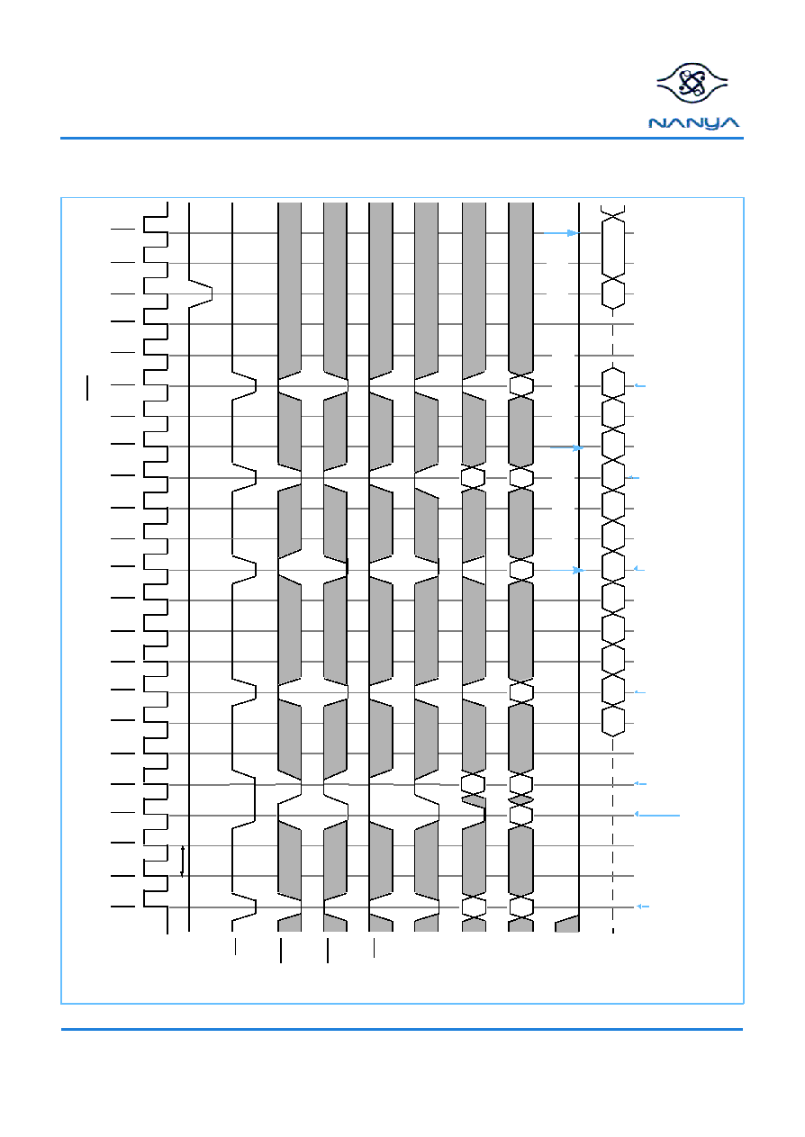
NT5SV32M4CT
NT5SV16M8CT
NT5SV8M16CT
128Mb Synchronous DRAM
REV 1.0
May, 2001
60
©
NANYA TECHNOLOGY CORP
. All rights reserved.
NANYA TECHNOLOGY CORP. reserves the right to change Products and Specifications without notice.
Auto Precharge after Read Burst
\
C
K
C
K
E
C
S
D
Q
R
A
S
C
A
S
W
E
*
B
S
1
D
Q
M
T
2
T
3
T
4
T
0
T
1
T
6
T
7
T
8
T
9
T
5
T
1
1
T
1
2
T
1
3
T
1
4
T
1
0
T
1
6
T
1
7
T
1
8
T
1
9
T
1
5
T
2
2
T
2
0
T
2
1
H
i
-
Z
A
1
0
A
0
-
A
9
,
t
C
K
3
H
i
g
h
R
e
a
d
w
i
t
h
A
u
t
o
P
r
e
c
h
a
r
g
e
C
o
m
m
a
n
d
B
a
n
k
1
C
B
y
S
t
a
r
t
A
u
t
o
P
r
e
c
h
a
r
g
e
B
a
n
k
1
S
t
a
r
t
A
u
t
o
P
r
e
c
h
a
r
g
e
B
a
n
k
0
A
x
3
A
x
2
A
x
0
A
x
1
B
x
3
B
x
2
B
x
0
B
x
1
A
y
3
A
y
2
A
y
0
A
y
1
A
c
t
i
v
a
t
e
C
o
m
m
a
n
d
B
a
n
k
0
R
A
x
R
A
x
R
e
a
d
w
i
t
h
A
u
t
o
P
r
e
c
h
a
r
g
e
C
o
m
m
a
n
d
B
a
n
k
1
C
B
x
R
e
a
d
w
i
t
h
A
u
t
o
P
r
e
c
h
a
r
g
e
C
o
m
m
a
n
d
B
a
n
k
0
A
c
t
i
v
a
t
e
C
o
m
m
a
n
d
B
a
n
k
1
R
B
x
C
A
x
R
B
x
A
c
t
i
v
a
t
e
C
o
m
m
a
n
d
B
a
n
k
1
R
e
a
d
C
o
m
m
a
n
d
B
a
n
k
0
R
B
y
C
A
y
R
B
y
B
y
0
B
y
1
*
B
S
0
=
"
L
"
B
a
n
k
2
,
3
=
I
d
l
e
S
t
a
r
t
B
a
n
k
1
A
u
t
o
P
r
e
c
h
a
r
g
e
(
B
u
r
s
t
l
e
n
g
t
h
=
4
,
C
A
S
l
a
t
e
n
c
y
=
3
;
t
R
C
D
,
t
R
P
=
3
)
A
1
1
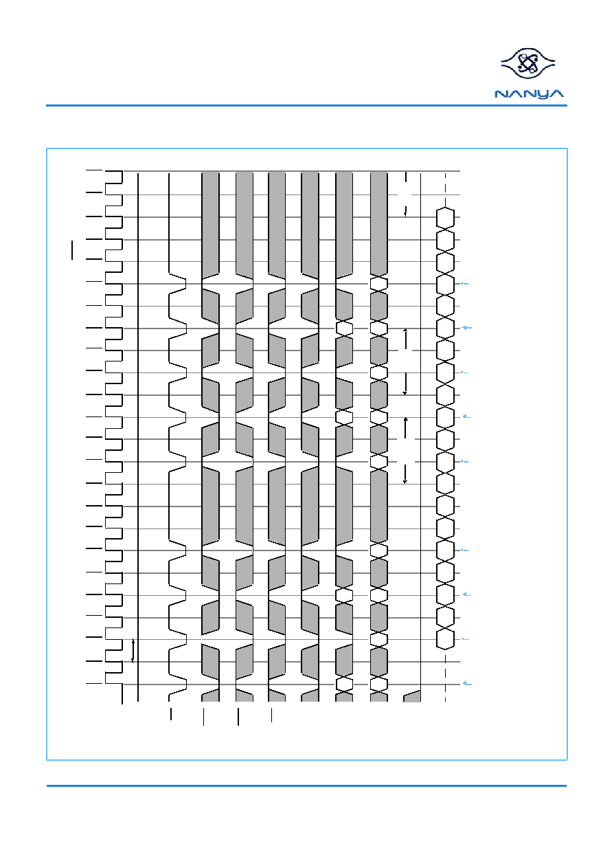
NT5SV32M4CT
NT5SV16M8CT
NT5SV8M16CT
128Mb Synchronous DRAM
REV 1.0
May, 2001
61
©
NANYA TECHNOLOGY CORP
. All rights reserved.
NANYA TECHNOLOGY CORP. reserves the right to change Products and Specifications without notice.
Auto Precharge after Write Burst
\
C
K
C
K
E
C
S
D
Q
R
A
S
C
A
S
W
E
*
B
S
1
D
Q
M
T
2
T
3
T
4
T
0
T
1
T
6
T
7
T
8
T
9
T
5
T
1
1
T
1
2
T
1
3
T
1
4
T
1
0
T
1
6
T
1
7
T
1
8
T
1
9
T
1
5
T
2
2
T
2
0
T
2
1
H
i
-
Z
A
1
0
A
0
-
A
9
,
t
C
K
2
H
i
g
h
W
r
i
t
e
w
i
t
h
A
u
t
o
P
r
e
c
h
a
r
g
e
C
o
m
m
a
n
d
B
a
n
k
1
C
B
y
A
c
t
i
v
a
t
e
C
o
m
m
a
n
d
B
a
n
k
1
R
B
x
R
B
x
W
r
i
t
e
w
i
t
h
A
u
t
o
P
r
e
c
h
a
r
g
e
C
o
m
m
a
n
d
B
a
n
k
1
C
B
x
D
A
x
3
D
A
x
2
D
A
x
1
D
A
x
0
D
B
x
3
D
B
x
2
D
B
x
1
D
B
x
0
D
A
y
3
D
A
y
2
D
A
y
1
D
A
y
0
D
B
y
3
D
B
y
2
D
B
y
1
D
B
y
0
D
A
z
3
D
A
z
2
D
A
z
1
D
A
z
0
A
c
t
i
v
a
t
e
C
o
m
m
a
n
d
B
a
n
k
0
R
A
z
R
A
z
W
r
i
t
e
C
o
m
m
a
n
d
B
a
n
k
0
C
A
x
W
r
i
t
e
w
i
t
h
A
u
t
o
P
r
e
c
h
a
r
g
e
C
o
m
m
a
n
d
B
a
n
k
0
C
A
y
A
c
t
i
v
a
t
e
C
o
m
m
a
n
d
B
a
n
k
1
R
B
y
R
B
y
A
c
t
i
v
a
t
e
C
o
m
m
a
n
d
B
a
n
k
0
R
A
x
R
A
x
W
r
i
t
e
w
i
t
h
A
u
t
o
P
r
e
c
h
a
r
g
e
C
o
m
m
a
n
d
B
a
n
k
0
C
A
z
*
B
S
0
=
"
L
"
B
a
n
k
2
,
3
=
I
d
l
e
A
1
1
t
D
A
L
t
D
A
L
N
u
m
b
e
r
o
f
c
l
o
c
k
s
d
e
p
e
n
d
s
o
n
c
l
o
c
k
c
y
c
l
e
a
n
d
s
p
e
e
d
s
o
r
t
.
S
e
e
t
h
e
C
l
o
c
k
F
r
e
q
u
e
n
c
y
a
n
d
L
a
t
e
n
c
y
t
a
b
l
e
.
B
a
n
k
m
a
y
b
e
r
e
a
c
t
i
v
a
t
e
d
a
t
t
h
e
c
o
m
p
l
e
t
i
o
n
o
f
t
D
A
L
.
t
D
A
L
(
B
u
r
s
t
l
e
n
g
t
h
=
4
,
C
A
S
l
a
t
e
n
c
y
=
2
)

NT5SV32M4CT
NT5SV16M8CT
NT5SV8M16CT
128Mb Synchronous DRAM
REV 1.0
May, 2001
62
©
NANYA TECHNOLOGY CORP
. All rights reserved.
NANYA TECHNOLOGY CORP. reserves the right to change Products and Specifications without notice.
Burst Read and Single Write Operation
\
C
K
C
K
E
C
S
D
Q
0
-
D
Q
7
R
A
S
C
A
S
W
E
*
B
S
1
L
D
Q
M
A
1
0
A
0
-
A
9
,
D
Q
8
-
D
Q
1
5
U
D
Q
M
T
2
T
3
T
4
T
0
T
1
T
6
T
7
T
8
T
9
T
5
T
1
1
T
1
2
T
1
3
T
1
4
T
1
0
T
1
6
T
1
7
T
1
8
T
1
9
T
1
5
T
2
2
T
2
0
T
2
1
H
i
-
Z
t
C
K
2
A
c
t
i
v
a
t
e
C
o
m
m
a
n
d
B
a
n
k
0
R
A
v
R
A
v
C
A
v
R
e
a
d
C
o
m
m
a
n
d
B
a
n
k
0
S
i
n
g
l
e
W
r
i
t
e
C
o
m
m
a
n
d
B
a
n
k
0
C
A
w
H
i
g
h
C
A
y
R
e
a
d
C
o
m
m
a
n
d
B
a
n
k
0
A
v
0
D
A
w
0
H
i
-
Z
A
v
2
A
v
1
A
v
3
D
A
x
0
A
v
2
A
v
1
A
y
2
D
A
w
0
A
y
0
A
y
3
A
v
0
A
v
3
S
i
n
g
l
e
W
r
i
t
e
C
o
m
m
a
n
d
B
a
n
k
0
A
y
3
S
i
n
g
l
e
W
r
i
t
e
C
o
m
m
a
n
d
B
a
n
k
0
D
A
z
0
D
A
z
0
C
A
x
C
A
z
L
o
w
e
r
B
y
t
e
i
s
m
a
s
k
e
d
A
y
0
A
y
1
U
p
p
e
r
B
y
t
e
i
s
m
a
s
k
e
d
L
o
w
e
r
B
y
t
e
i
s
m
a
s
k
e
d
*
B
S
0
=
"
L
"
B
a
n
k
2
,
3
=
I
d
l
e
(
B
u
r
s
t
l
e
n
g
t
h
=
4
,
C
A
S
l
a
t
e
n
c
y
=
2
)
A
1
1

NT5SV32M4CT
NT5SV16M8CT
NT5SV8M16CT
128Mb Synchronous DRAM
REV 1.0
May, 2001
63
©
NANYA TECHNOLOGY CORP
. All rights reserved.
NANYA TECHNOLOGY CORP. reserves the right to change Products and Specifications without notice.
CS Function
(Only CS signal needs to be asserted at minimum rate)
\
C
K
C
K
E
C
S
D
Q
R
A
S
C
A
S
W
E
B
S
0
,
B
S
1
D
Q
M
T
2
T
3
T
4
T
0
T
1
T
6
T
7
T
8
T
9
T
5
T
1
1
T
1
2
T
1
3
T
1
4
T
1
0
T
1
6
T
1
7
T
1
8
T
1
9
T
1
5
T
2
2
T
2
0
T
2
1
H
i
-
Z
A
1
0
A
0
-
A
9
,
A
1
1
t
C
K
3
R
A
x
L
o
w
R
A
x
C
A
x
C
A
y
R
e
a
d
C
o
m
m
a
n
d
B
a
n
k
A
W
r
i
t
e
C
o
m
m
a
n
d
B
a
n
k
A
A
c
t
i
v
a
t
e
C
o
m
m
a
n
d
B
a
n
k
A
P
r
e
c
h
a
r
g
e
C
o
m
m
a
n
d
B
a
n
k
A
A
x
0
D
A
y
0
D
A
y
3
D
A
y
2
D
A
y
1
A
x
3
A
x
2
A
x
1
t
R
C
D
t
D
P
L
(
a
t
1
0
0
M
H
z
B
u
r
s
t
L
e
n
g
t
h
=
4
,C
A
S
L
a
t
e
n
c
y
=
3
,
t
R
C
D
,
t
R
P
=
3
)

NT5SV32M4CT
NT5SV16M8CT
NT5SV8M16CT
128Mb Synchronous DRAM
REV 1.0
May, 2001
64
©
NANYA TECHNOLOGY CORP
. All rights reserved.
NANYA TECHNOLOGY CORP. reserves the right to change Products and Specifications without notice.
Package Dimensions
(400mil; 54 lead; Thin Small Outline Package)
Lead #1
0.80 Basic
0.35
1
0
.
1
6
±
0
.
1
3
22.22
±
0.13
1
1
.
7
6
±
0
.
2
0
-
0.05
+ 0.10
0.71REF
Detail A
0.10
Seating Plane
Detail A
0.5
±
0.1
0.05 Min
1
.
2
0
M
a
x
0.25 Basic
Gage Plane

NT5SV32M4CT
NT5SV16M8CT
NT5SV8M16CT
128Mb Synchronous DRAM
REV 1.0
May, 2001
65
©
NANYA TECHNOLOGY CORP
. All rights reserved.
NANYA TECHNOLOGY CORP. reserves the right to change Products and Specifications without notice.
Revision Log
Rev. Date
Contents of Modification
05/2000
Initial release
03/2001
Removed stack package and stack references throughout the document.
Added a new AC timing parameter t
RFC
to define the Auto Refresh to Activate Bank/Auto Refresh command period.
Updated timing diagrams to reflect the change.
Updated I
CC2P
and I
CC2PS
to 2mAmps.
05/2001
Removed Preliminary

Nanya Technology Corporation.
All rights reserved.
Printed in Taiwan, R.O.C. May 2001
The following are trademarks of NANYA TECHNOLOGY CORPORATION in R.O.C , or other countries, or both.
NANYA NANYA logo
Other company, product and service names may be trademarks or services maeks of others.
NANYA TECHNOLOGY CORPORATION (NTC) reserves the right to make changes without notice. NTC warrants performance
of its semiconductor products and related software to the specifications applicable at the time of sale in accordance with NTC's
standard warranty. Testing and other quality control techniques are utilize to the extent NTC deems necessary to support this
warranty. Specific testing of all parameters of each device is not necessarily performed, except those mandated by government
requirements.
Certain applications using semiconductor products may involve potential risks of death, personal injury, or severe property or
environmental damage ("Critical Applications").
NTC SEMICONDUCTOR PRODUCTS ARE NOT DESIGNED, INTEND, AUTHORIZED, OR WARRANTED TO BE SUITABLE
FOR USE IN LIFE-SUPPORT APPLICATIONS, DEVICES OR SYSTEMS OR OTHER CRITICAL APPLICATIONS.
Inclusion of NTC products in such applications is understood to be fully at the risk of the customer. Use of NTC products in such
applications requires the written approval of an appropriate NTC officer. Question concerning potential risk applications should
be directed to NTC through a local sales office.
In order to minimize risks associated with the customer's applications, adequate design and operating safeguards should be
provided by customer to minimize the inherent or procedural hazards.
NTC assumes no liability of applications assistance, customer product design, software performance, or infringement of patents
or services described herein. Nor does NTC warrant or represent that any license, either express or implied, is granted under
any patent right, copyright, mask work right, or other intellectual property right of NTC covering or relating to any combination,
machine, or process in which such semiconductor products or services might be or are used.
NANYA TECHNOLOGY CORPORATION
HWA YA Technology Park
669, FU HSING 3rd Rd., Kueishan,
Taoyuan, Taiwan, R.O.C.
The NANYA TECHNOLOGY CORPORATION home page can be found at
http:\\www.nanya.com
Æ
©