Document No. D14856EJ2V0DS00 (2nd edition)
Date Published April 2002 N CP(K)
Printed in Japan
SILICON POWER TRANSISTOR
2SA1129
PNP SILICON EPITAXIAL TRANSISTOR
FOR LOW-FREQUENCY POWER AMPLIFIERS AND MID-SPEED SWITCHING
DATA SHEET
The information in this document is subject to change without notice. Before using this document, please
confirm that this is the latest version.
Not all devices/types available in every country. Please check with local NEC representative for
availability and additional information.
©
2002
The 2SA1129 is a mold power transistor developed for mid-speed
switching, and is ideal for use as a ramp driver.
FEATURES
∑ Large current capacity with small package: I
C(DC)
=
-7.0 A
∑ Low collector saturation voltage:
V
CE(sat)
=
-0.3 V MAX. @I
C
=
-3.0 A, IB = -0.1 A
∑ Complementary transistor: 2SC2654
ABSOLUTE MAXIMUM RATINGS (T
A
= 25
∞
∞
∞
∞C)
Parameter
Symbol
Conditions
Ratings
Unit
Collector to base voltage
V
CBO
-30
V
Collector to emitter voltage
V
CEO
-30
V
Emitter to base voltage
V
EBO
-7.0
V
Collector current (DC)
I
C(DC)
-7.0
A
Collector current (pulse)
I
C(pulse)
PW
300
µs,
duty cycle
10%
-15
A
Base current (DC)
I
B(DC)
-3.5
A
T
C
= 25
∞C
40
W
Total power dissipation
P
T
T
A
= 25
∞C
1.5
W
Junction temperature
T
j
150
∞C
Storage temperature
T
stg
-55 to +150
∞C
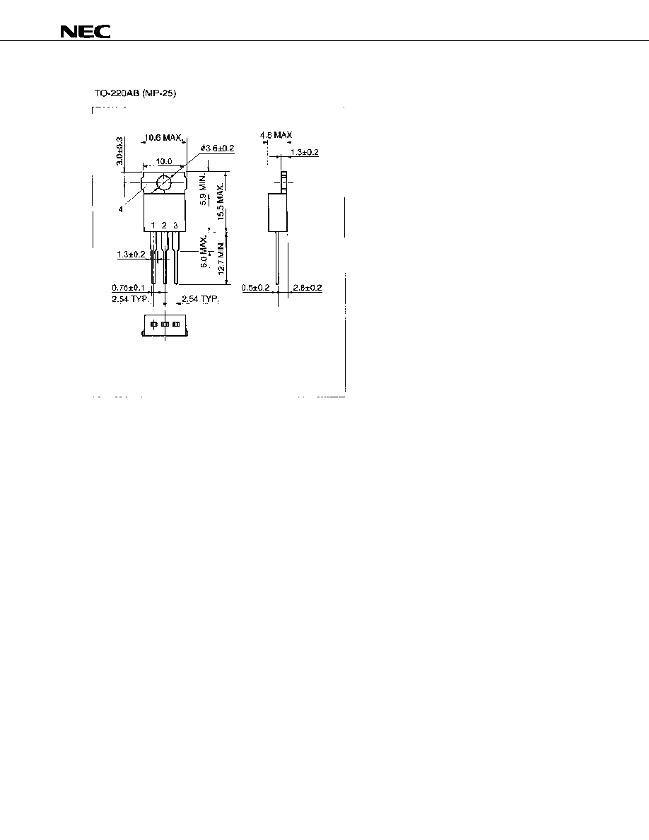
ORDERING INFORMATION
Part No.
Package
2SA1129
TO-220AB
(TO-220AB)

Data Sheet D14856EJ2V0DS
2
2SA1129
ELECTRICAL CHARACTERISTICS (T
A
= 25
∞
∞
∞
∞C)
Parameter
Symbol
Conditions
MIN.
TYP.
MAX.
Unit
Collector cutoff current
I
CBO
V
CB
=
-30 V, I
E
= 0 A
-10
µA
Emitter cutoff current
I
EBO
V
EB
=
-5.0 V, I
C
= 0 A
-10
µA
DC current gain
h
FE1
V
CE
=
-1.0 V, I
C
=
-3.0 A
Note
40
200
DC current gain
h
FE2
V
CE
=
-1.0 V, I
C
=
-5.0 A
Note
20
Collector saturation voltage
V
CE(sat)1
I
C
=
-3.0 A, I
B
=
-0.1 A
Note
-0.3
V
Collector saturation voltage
V
CE(sat)2
I
C
=
-5.0 A, I
B
=
-0.5 A
Note
-0.6
V
Base saturation voltage
V
BE(sat)1
I
C
=
-3.0 A, I
B
=
-0.1 A
Note
-1.5
V
Base saturation voltage
V
BE(sat)2
I
C
=
-5.0 A, I
B
=
-0.5 A
Note
-2.0
V
Turn-on time
t
on
1.0
µs
Storage time
t
stg
2.5
µs
Fall time
t
f
I
C
=
-5.0 A, R
L
= 4.0
,
I
B1
=
-I
B2
=
-0.5 A, V
CC
-20 V
PW = 50
µs, duty cycle = 2%
1.0
µs
Note Pulse test PW
350
µs, duty cycle 2%
h
FE
CLASSIFICATION
Marking
M
L
K
h
FE1
40 to 80
60 to 120
100 to 200
SWITCHING TIME (t
on
, t
stg
, t
f
) TEST CIRCUIT
Base current
waveform
Collector current
waveform

Data Sheet D14856EJ2V0DS
3
2SA1129
TYPICAL CHARACTERISTICS (T
A
= 25
∞
∞
∞
∞C)
T
o
t
a
l
P
o
w
e
r
Di
s
s
i
pa
t
i
on
P
T
(W)
$PELHQW 7HPSHUDWXUH 7
$
∞&�
&DVH 7HPSHUDWXUH 7
&
∞&�
&ROOHFWRU WR (PLWWHU 9ROWDJH 9
&(
9�
Col
l
e
c
t
or Current
I
C
(
A
)
Trans
i
ent
Therm
a
l
Res
i
s
t
an
c
e
r
t
h
(j
-c)
(
∞
C/W)
3XOVH :LGWK 3: PV�
&ROOHFWRU WR (PLWWHU 9ROWDJH 9
&(
9�
Col
l
e
c
t
or Current
I
C
(
A
)
Derat
i
ng dT
(
%
)
PP DOXPLQXP ERDUG
QR LQVXODWLQJ ERDUG
JUHDVH FRDWLQJ QDWXUDO
DLU FRROLQJ
:LWK LQILQLWH KHDWVLQN