Document No. D15587EJ2V0DS00 (2nd edition)
Date Published April 2002 N CP(K)
Printed in Japan
SILICON POWER TRANSISTOR
2SA1645, 2SA1645-Z
PNP SILICON EPITAXIAL
TRANSISTOR
FOR HIGH-SPEED SWITCHING
DATA SHEET
The information in this document is subject to change without notice. Before using this document, please
confirm that this is the latest version.
Not all devices/types available in every country. Please check with local NEC representative for
availability and additional information.
©
2002
The 2SA1645 is a mold power transistor developed for high-
speed switching and features a very low collector-to-emitter
saturation voltage. This transistor is ideal for use in switching
power supplies, DC/DC converters, motor drivers, solenoid drivers,
and other low-voltage power supply devices, as well as for high-
current switching.
FEATURES
∑ Fast switching speed
∑ Low collector-to-emitter saturation voltage:
V
CE(sat)
=
-0.3 V MAX. @I
C
=
-4 A
ABSOLUTE MAXIMUM RATINGS (Ta = 25
∞
∞
∞
∞C)
Parameter
Symbol
Conditions
Ratings
Unit
Collector to base voltage
V
CBO
-150
V
Collector to emitter
voltage
V
CEO
-100
V
Emitter to base voltage
V
EBO
-7.0
V
Collector current
I
D(DC)
-7.0
A
Collector current
I
C(pulse)
PW
300
µs,
Duty Cycle
10%
-14
A
Base current
I
B(DC)
-3.5
A
Total power dissipation
P
T
Tc = 25
∞C
35
W
Total power dissipation
P
T
Ta = 25
∞C
1.5
W
Junction temperature
T
j
150
∞C
Storage temperature
T
stg
-55 to
+150
∞C
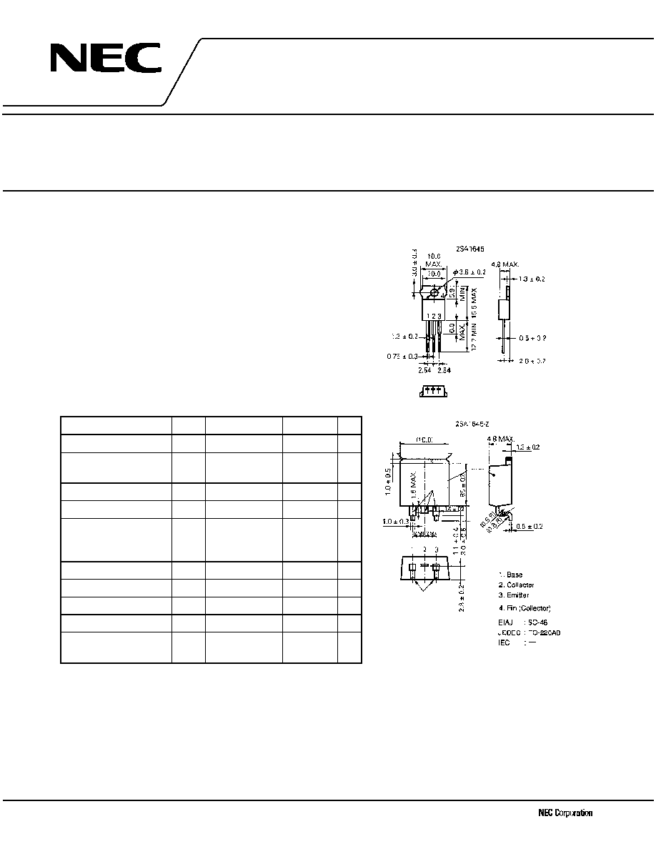
PACKAGE DRAWING (UNIT: mm)
$UHD ZLWKRXW
VROGHU SODWLQJ
0DLQ
XQLW
$UHD ZLWKRXW
VROGHU SODWLQJ
(OHFWURGH &RQQHFWLRQ
/HDG
ZLUH
$UHD ZLWKRXW
VROGHU SODWLQJ
9DOXHV LQ SDUHQWKHVHV
DUH VWDQGDUG
0DUNLQJ
VLGH

Data Sheet D15587EJ2V0DS
2
2SA1645, 2SA1645-Z
ELECTRICAL CHARACTERISTICS (Ta = 25
∞
∞
∞
∞C)
Parameter
Symbol
Conditions
MIN.
TYP.
MAX.
Unit
Collector cutoff current
I
CBO
V
CB
=
-100 V, I
E
= 0
-10
µA
Emitter cutoff current
I
EBO
V
EB
=
-5 V, I
C
= 0
-10
µA
DC current gain
h
FE1
*
V
CE
=
-2 V, I
C
=
-0.5 A
100
-
DC current gain
h
FE2
*
V
CE
=
-2 V, I
C
=
-1.5 A
100
400
-
DC current gain
h
FE3
*
V
CE
=
-2 V, I
C
=
-4 A
60
-
Collector saturation voltage
V
CE(sat)1
*
I
C
=
-4 A, I
B
=
-0.2 A
-0.3
V
Collector saturation voltage
V
CE(sat)2
*
I
C
=
-6 A, I
B
=
-0.3 A
-0.5
V
Base saturation voltage
V
BE(sat)1
*
I
C
=
-4 A, I
B
=
-0.2 A
-1.2
V
Base saturation voltage
V
BE(sat)2
*
I
C
=
-6 A, I
B
=
-0.3 A
-1.5
V
Gain bandwidth product
f
T
V
CE
=
-10 V, I
C
=
-1.5 A
150
MHz
Collector capacitance
C
ob
V
CB
=
-10 V, I
E
= 0, f = 1 MHz
150
pF
Turn-on time
t
on
0.3
µs
Storage time
t
stg
1.5
µs
Fall time
t
f
I
C
=
-4 A, I
B1
=
-I
B2
=
-0.2 A,
R
L
= 12.5
, V
CC
=
-50 V
Refer to the test circuit.
0.4
µs
* Pulse test PW
350
µs, duty cycle 2%
h
FE
CLASSIFICATION
Marking
M
L
K
h
FE2
100 to 200
150 to 300
200 to 400
SWITCHING TIME TEST CIRCUIT
Base current
waveform
Collector current
waveform

Data Sheet D15587EJ2V0DS
3
2SA1645, 2SA1645-Z
TYPICAL CHARACTERISTICS (Ta = 25
∞
∞
∞
∞C)
T
o
ta
l
P
o
we
r
Dis
s
i
p
a
ti
o
n
P
T
(W
)
Case Temperature T
C
(
∞
C)
Collector to Emitter Voltage V
CE
(V)
Co
l
l
e
c
to
r
Cu
r
r
e
n
t
I
C
(
A
)
Co
l
l
e
c
to
r
Cu
r
r
e
n
t
I
C
(
m
A)
Collector to Emitter Voltage V
CE
(V)
Collector Current I
C
(A)
DC Cu
rr
e
n
t Ga
i
n
h
FE
I
C
De
r
a
ti
n
g
d
T
(%
)
Case Temperature T
C
(
∞
C)
Collector Current I
C
(mA)
C
o
l
l
ec
t
o
r
S
a
t
u
r
a
t
i
o
n
V
o
l
t
ag
e
V
CE
(
s
a
t
)
(V)
Pulse test
Pulse test
Single pulse

