1998
©
Document No. D16145EJ1V0DS00 (1st edition)
Date Published April 2002 N CP(K)
Printed in Japan
SILICON TRANSISTOR
2SA1897
PNP SILICON EPITAXIAL TRANSISTOR
FOR LOW-FREQUENCY POWER AMPLIFIERS AND MID-SPEED SWITCHING
DATA SHEET
2002
The information in this document is subject to change without notice. Before using this document, please
confirm that this is the latest version.
Not all devices/types available in every country. Please check with local NEC representative for
availability and additional information.
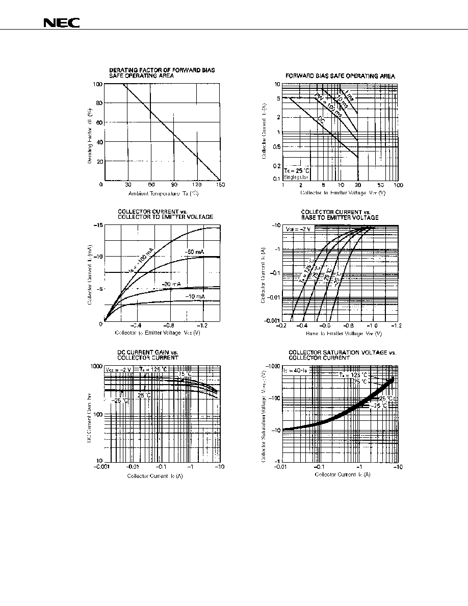
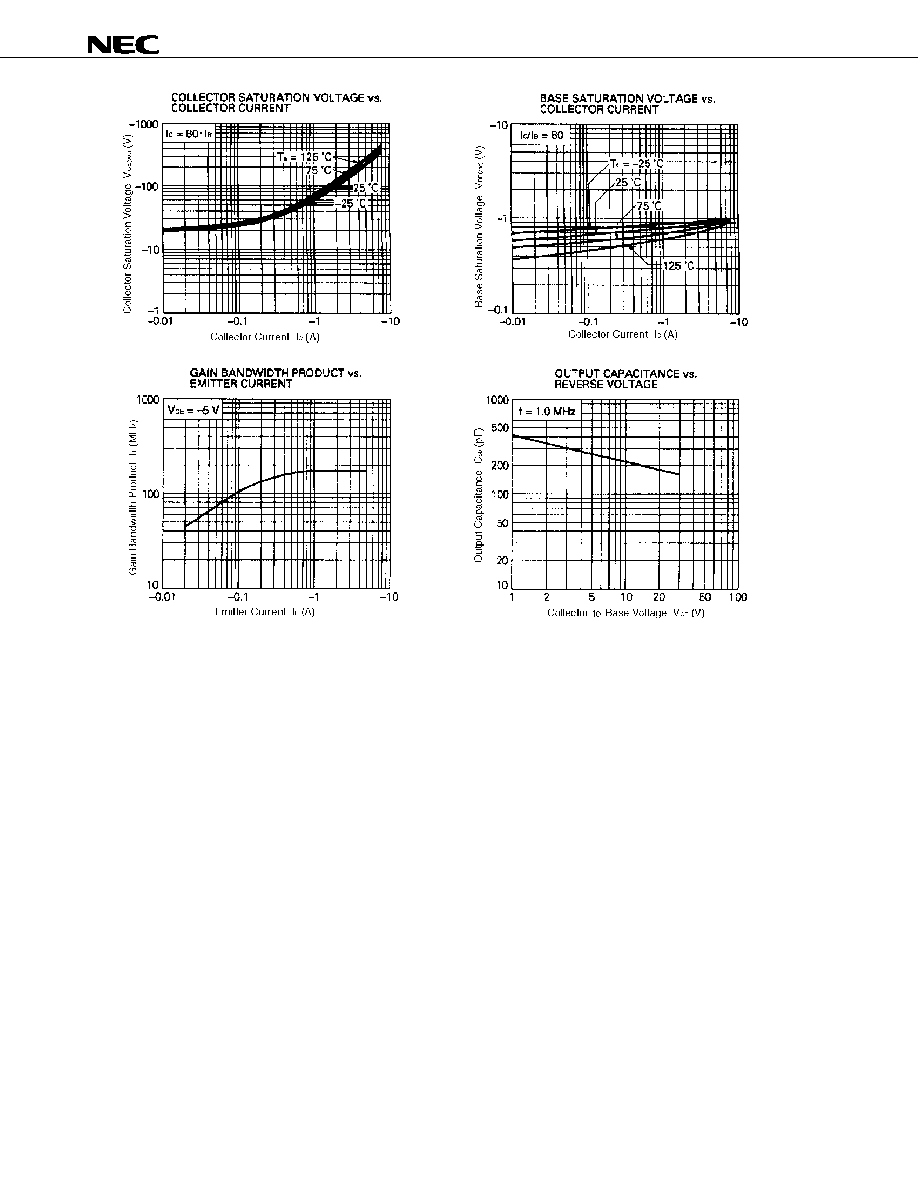
The 2SA1897 features a low saturation voltage and is available
for high current control in small dimension. This transistor is ideal
for high efficiency DC/DC converters due to fast switching speed.
FEATURES
∑
High current capacitance
∑
Low collector saturation voltage and high h
FE
∑
Insulation type package supportable for radial taping
QUALITY GRADES
∑ Standard
Please refer to "Quality Grades on NEC Semiconductor Devices"
(Document No. C11531E) published by NEC Corporation to
know the specification of quality grade on the devices and its
recommended applications.
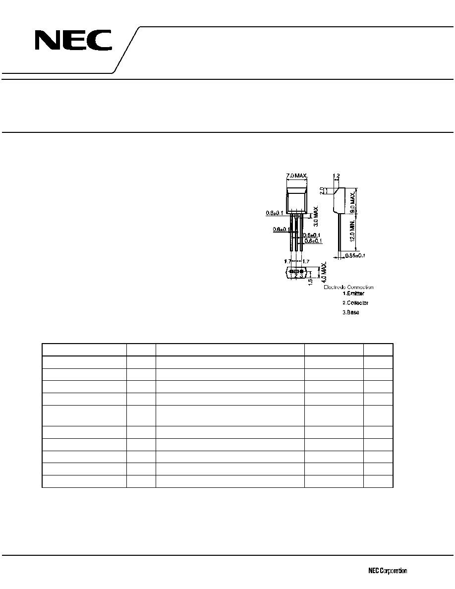
PACKAGE DRAWING (UNIT: mm)
ABSOLUTE MAXIMUM RATINGS (Ta = 25
∞
∞
∞
∞C)
Parameter
Symbol
Conditions
Ratings
Unit
Collector to base voltage
V
CBO
-30
V
Collector to emitter voltage
V
CEO
-20
V
Emitter to base voltage
V
EBO
-10
V
Collector current (DC)
I
C(DC)
T
C
= 25
∞C
-5.0
A
Collector current (pulse)
I
C(pulse)
PW
10 ms, duty cycle 50 %
T
C
= 25
∞C
-8.0
A
Base current (DC)
I
B(DC)
-0.5
A
Total power dissipation
P
T
1.0
W
Total power dissipation
P
T
T
C
= 25
∞C
6.0
W
Junction temperature
T
j
150
∞C
Storage temperature
T
stg
-55 to +150
∞C