The information in this document is subject to change without notice. Before using this document, please
confirm that this is the latest version.
Not all devices/types available in every country. Please check with local NEC representative for
availability and additional information.
1998
©
Document No. D16129EJ2V0DS00 (2nd edition)
Date Published July 2002 N CP(K)
Printed in Japan
SILICON TRANSISTOR
2SB1453
PNP SILICON EPITAXIAL POWER TRANSISTOR
FOR HIGH-SPEED SWITCHING
DATA SHEET
2002
The 2SB1453 is a power transistor that can directly drive from
the IC output. This transistor is ideal for motor drivers and solenoid
drivers in such as OA and FA equipment.
In addition, a small resin-molded insulation type package
contributes to high-density mounting and reduction of mounting
cost.
FEATURES
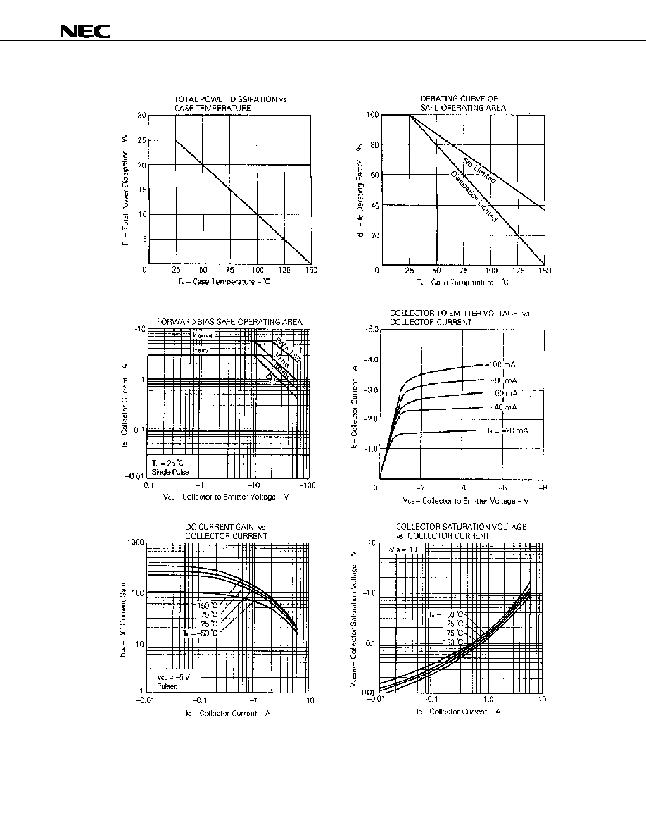
∑ High DC current amplifier ratio
h
FE
100 (V
CE
=
-5 V, I
C
=
-0.5 A)
∑ Mold package that does not require an insulating board or
insulation bushing
ABSOLUTE MAXIMUM RATINGS (Ta = 25
∞
∞
∞
∞C)
Parameter
Symbol
Ratings
Unit
Collector to base voltage
V
CBO
-60
V
Collector to emitter voltage
V
CEO
-60
V
Emitter to base voltage
V
EBO
-7.0
V
Collector current (DC)
I
C(DC)
-3.0
A
Collector current (pulse)
I
C(pulse)
*
-6.0
A
Base current (DC)
I
B(DC)
-1.0
A
Total power dissipation
P
T
(Tc = 25
∞C)
25
W
Total power dissipation
P
T
(Ta = 25
∞C)
2.0
W
Junction temperature
T
j
150
∞C
Storage temperature
T
stg
-55 to +150
∞C
* PW
10 ms, duty cycle 50%
PACKAGE DRAWING (UNIT: mm)
Electrode Connection
1. Base
2. Collector
3. Emitter
Data Sheet D16129EJ2V0DS
2
2SB1453
ELECTRICAL CHARACTERISTICS (Ta = 25
∞
∞
∞
∞C)
Parameter
Symbol
Conditions
MIN.
TYP.
MAX.
Unit
Collector cutoff current
I
CBO
V
CB
=
-60 V, I
E
= 0
-10
µA
DC current gain
h
FE1
**
V
CE
=
-5.0 V, I
C
=
-0.5 A
100
400
-
DC current gain
h
FE2
**
V
CE
=
-5 V, I
C
=
-3 A
20
-
Collector saturation voltage
V
CE(sat)
**
I
C
=
-3.0 A, I
B
=
-300 mA
-1.0
V
Base saturation voltage
V
BE(sat)
**
I
C
=
-3.0 A, I
B
=
-300 mA
-2.0
V
Gain bandwidth product
f
T
V
CE
=
-5.0 V, I
C
=
-0.5 A
5
MHz
Collector capacitance
C
ob
V
CB
=
-10 V, I
E
= 0, f = 1.0 MHz
80
pF
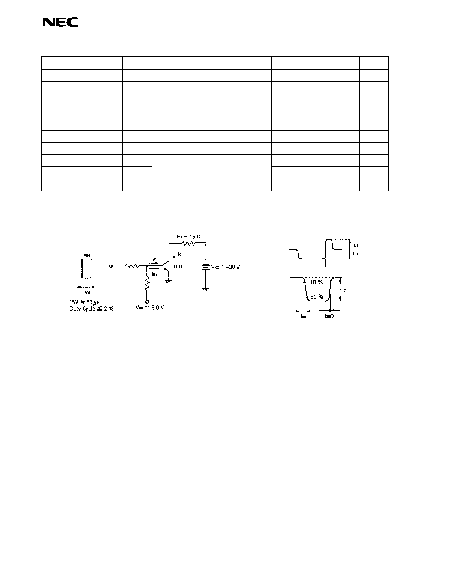
Turn-on time
t
on
0.4
µs
Storage time
t
stg
1.7
µs
Fall time
t
f
I
C
=
-2.0 A, I
B1
=
-I
B2
=
-200 mA,
R
L
= 15
, V
CC
-30 V
Refer to the test circuit.
0.5
µs
** Pulse test PW
350
µs, duty cycle 2%
SWITCHING TIME (t
on
, t
stg
, t
f
) TEST CIRCUIT
Base current
waveform
Collector current
waveform