1998
©
Document No. D13533EJ3V0DS00 (3rd edition)
Date Published April 2002 N CP(K)
Printed in Japan
THYRISTORS
3P4MH, 3P6MH
3 A MOLD SCR
DATA SHEET
2002
The information in this document is subject to change without notice. Before using this document, please
confirm that this is the latest version.
Not all devices/types available in every country. Please check with local NEC representative for
availability and additional information.
The 3P4MH and 3P6MH are P-gate fully diffused mold
SCRs with an average on-current of 3 A. The repeat peak off-
voltages (and reverse voltages) are 400 V and 600 V.
FEATURES
∑ This transistor features a small and lightweight package and
is easy to handle even on the mounting surface due to its
TO-202AA dimensions. Processing of lead wires and
heatsink (tablet) using jigs is also possible.
∑ Employs flame-retardant epoxy resin (UL94V-0).
APPLICATIONS
Noncontact switches of consumer electronic euipments,
electric equipments, audio quipments, and light indutry
equipements
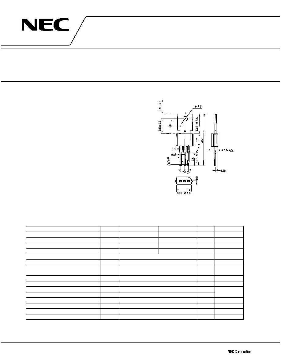
PACKAGE DRAWING (UNIT: mm)
ABSOLUTE MAXIMUM RATINGS (Ta = 25
∞
∞
∞
∞C)
Parameter
Symbol
3P4MH
3P6MH
Ratings
Unit
Non-repetitive peak reverse voltage
V
RSM
500
700
V
R
GK
= 1 k
Non-repetitive peak off-state voltage
V
DSM
500
700
V
R
GK
= 1 k
Repetitive peak reverse voltage
V
RRM
400
600
V
R
GK
= 1 k
Repetitive peak off-voltage
V
DRM
400
600
V
R
GK
= 1 k
Average on-state current
I
T(AV)
3 (Tc = 87
∞C, Single half-wave,
= 180∞)
A
Refer to Figure 11.
Effective on-state current
I
T(RMS)
4.7
A
-
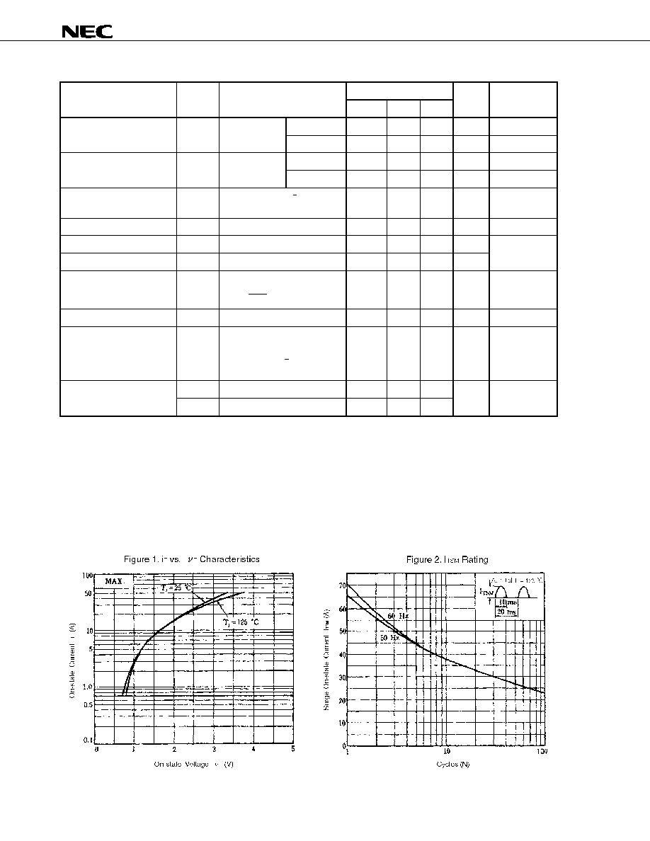
Surge on-state current
I
TSM
65 (f = 50 Hz, Sine half-wave, 1 cycle)
70 (f = 60 Hz, Sine half-wave, 1 cycle)
A
Refer to Figure 2.
Fusing current
i
t
2
dt
20 (1 ms
t10 ms)
A
2
s
-
Critical rate of rise of on-state current
dI
T
/dt
50
A/
µs
-
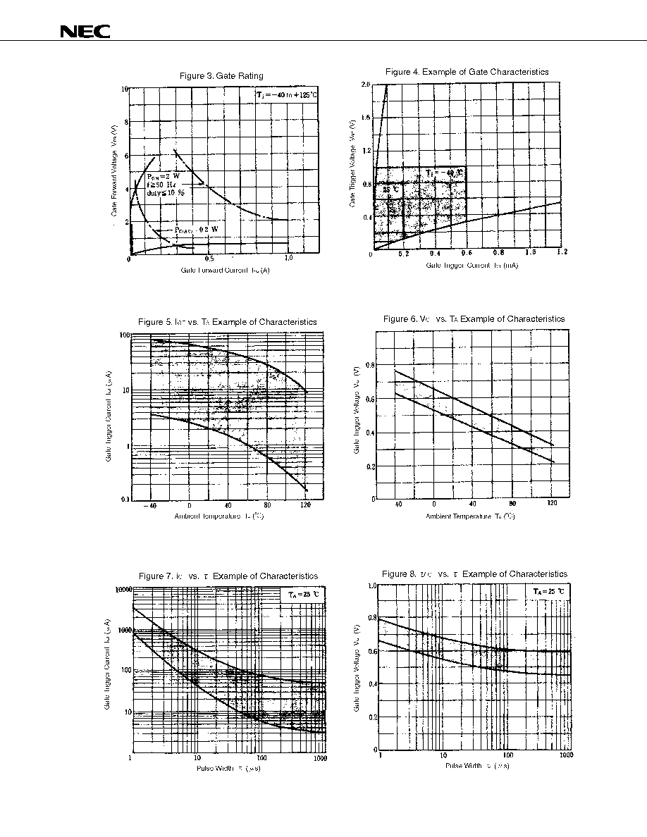
Peak gate power dissipation
P
GM
2 (f
50 Hz, Duty10%)
W
Refer to Figure 3.
Average gate power dissipation
P
G(AV)
0.2
W
Peak gate forward current
I
FGM
1 (f
50 Hz, Duty10%)
A
-
Peak gate reverse voltage
V
RGM
6
V
-
Junction temperature
T
j
-40 to +125
∞C
-
Storage temperature
T
stg
-55 tp +150
∞C
-
Electrode connection
<1>Cathode
<2>Anode
<3>Gate
Standard weight: 1.4
*TC test bench-mark