The information in this document is subject to change without notice. Before using this document, please
confirm that this is the latest version.
Not all devices/types available in every country. Please check with local NEC representative for
availability and additional information.
©
1992
MOS INTEGRATED CIRCUIT
µ
µ
µ
µ
PD43257B
256K-BIT CMOS STATIC RAM
32K-WORD BY 8-BIT
DATA SHEET
Document No. M10693EJ7V0DS00 (7th edition)
Date Published June 2000 NS CP (K)
Printed in Japan
The mark
5
shows major revised points.
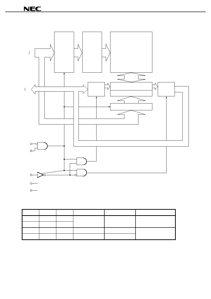
Description
The
µ
PD43257B is a high speed, low power, and 262,144 bits (32,768 words by 8 bits) CMOS static RAM.
Battery backup is available. And the
µ
PD43257B has two chip enable pins (/CE1, CE2) to extend the capacity.
The
µ
PD43257B is packed in 28-pin plastic DIP and 28-pin plastic SOP.
Features
∑
32,768 words by 8 bits organization
∑
Fast access time: 70, 85 ns (MAX.)
∑
Low V
CC
data retention: 2.0 V (MIN.)
∑
Two Chip Enable inputs: /CE1, CE2
Part number
Access time
Operating supply
Operating ambient
Supply current
ns (MAX.)
voltage
temperature
At operating
At standby
At data retention
V
∞C
mA (MAX.)
µ
A (MAX.)
µ
A (MAX.)
Note
µ
PD43257B-xxL
70, 85
4.5 to 5.5
0 to 70
45
50
3
µ
PD43257B-xxLL
45
15
2
Note
T
A
40
∞
C, V
CC
= 3.0 V
Version X
This Data sheet can be applied to the version X. This version is identified with its lot number. Letter X in the fifth
character position in a lot number signifies version X.
X
D43257B
Lot number
JAPAN

Data Sheet M10693EJ7V0DS00
3
µ
µ
µ
µ
PD43257B
Pin Configurations (Marking Side)
/xxx indicates active low signal.
28-PIN PLASTIC DIP (15.24 mm (600))
[
µ
µ
µ
µ
PD43257BCZ-xxL ]
[
µ
µ
µ
µ
PD43257BCZ-xxLL ]
A14
A12
A7
A6
A5
A4
A3
A2
A1
A0
I/O1
I/O2
I/O3
GND
V
CC
/WE
A13
A8
A9
A11
CE2
A10
/CE1
I/O8
I/O7
I/O6
I/O5
I/O4
1
2
3
4
5
6
7
8
9
10
11
12
13
14
28
27
26
25
24
23
22
21
20
19
18
17
16
15
A0 - A14
: Address inputs
I/O1 - I/O8
: Data inputs / outputs
/CE1
: Chip Enable 1
CE2
: Chip Enable 2
/WE
: Write Enable
V
CC
: Power supply
GND
: Ground
Remark Refer to Package Drawings for the 1-pin marking.

Data Sheet M10693EJ7V0DS00
4
µ
µ
µ
µ
PD43257B
28-PIN PLASTIC SOP (11.43 mm (450))
[
µ
µ
µ
µ
PD43257BGU-xxL ]
[
µ
µ
µ
µ
PD43257BGU-xxLL ]
A14
A12
A7
A6
A5
A4
A3
A2
A1
A0
I/O1
I/O2
I/O3
GND
V
CC
/WE
A13
A8
A9
A11
CE2
A10
/CE1
I/O8
I/O7
I/O6
I/O5
I/O4
1
2
3
4
5
6
7
8
9
10
11
12
13
14
28
27
26
25
24
23
22
21
20
19
18
17
16
15
A0 - A14
: Address inputs
I/O1 - I/O8
: Data inputs / outputs
/CE1
: Chip Enable 1
CE2
: Chip Enable 2
/WE
: Write Enable
V
CC
: Power supply
GND
: Ground
Remark Refer to Package Drawings for the 1-pin marking.