Document Outline
- COVER
- Features
- Ordering Information
- Pin Configuration
- Block Diagram
- Electrical Specifications
- Package Drawing
The information in this document is subject to change without notice. Before using this document, please
confirm that this is the latest version.
Not all devices/types available in every country. Please check with local NEC representative for
availability and additional information.
©
2001
MOS INTEGRATED CIRCUIT
MC-222244A-X
MCP (MULTI-CHIP PACKAGE) FLASH MEMORY AND SRAM
32M-BIT FLASH MEMORY AND 4M-BIT SRAM
DATA SHEET
Document No. M15318EJ2V0DS00 (2nd edition)
Date Published July 2001 NS CP (K)
Printed in Japan
The mark
5
5
5
5
shows major revised points.
Description
The MC-222244A-X is a stacked type MCP (Multi-Chip Package) of 33,554,432 bits (BYTE mode : 4,194,304 words
by 8 bits, WORD mode : 2,097,152 words by 16 bits) flash memory and 4,194,304 bits (BYTE mode : 524,288 words
by 8 bits, WORD mode : 262,144 words by 16 bits) static RAM.
The MC-222244A-X is packaged in a 77-pin TAPE FBGA.
Features
General Features
∑
Fast access time : t
ACC
= 85 ns (MAX.) (Flash Memory), t
AA
= 70 ns (MAX.) (SRAM)
∑
Supply voltage : V
CC
f / V
CC
s = 2.7 to 3.6 V
∑
Wide operating temperature : T
A
=
-
25 to +85
∞
C
Flash Memory Features
∑
Two bank organization enabling simultaneous execution of erase / program and read
∑
Bank organization : 2 banks (16M bits + 16M bits)
∑
Memory organization : 4,194,304 words
◊
8 bits (BYTE mode)
2,097,152 words
◊
16 bits (WORD mode)
∑
Sector organization : 71 sectors (8K bytes / 4K words
◊
8 sectors, 64K bytes / 32K words
◊
63 sectors)
∑
Boot sector allocated to the highest address (sector)
∑
3-state output
∑
Automatic program
∑
Program suspend / resume
∑
Unlock bypass program
∑
Automatic erase
∑
Chip erase
∑
Sector erase (sectors can be combined freely)
∑
Erase suspend / resume
∑
Program / Erase completion detection
∑
Detection through data polling and toggle bits
∑
Detection through RY (/BY) pin
∑
Sector group protection
∑
Any sector can be protected
∑
Any protected sector can be temporary unprotected
∑
Sectors can be used for boot application
∑
Hardware reset and standby using /RESET pin
∑
Automatic sleep mode
∑
Boot block sector protect by /WP (ACC) pin
∑
Conforms to common flash memory interface (CFI)
∑
Extra One Time Protect Sector provided

Data Sheet M15318EJ2V0DS
2
MC-222244A-X
SRAM Features
∑
Memory organization : 524,288 words
◊
8 bits (BYTE mode)
262,144 words
◊
16 bits (WORD mode)
∑
Supply current : At operating : 40 mA (MAX.)
At standby : 7
µ
A (MAX.)
∑
Two Chip Enable inputs : /CE1s, CE2s
∑
Byte data control : /LB, /UB
∑
Byte data select : CIOs
∑
Low V
CC
data retention : 1.0 to 3.6 V
Ordering Information
Part number
Flash Memory
Flash Memory
SRAM
Package
Boot sector
Access time
Access time
ns (MAX.)
ns (MAX.)
MC-222244AF9-B85X-BT3
Highest address (sector)
85
70
77-pin TAPE FBGA (12
◊
7)
(T type)
Data Sheet M15318EJ2V0DS
3
MC-222244A-X
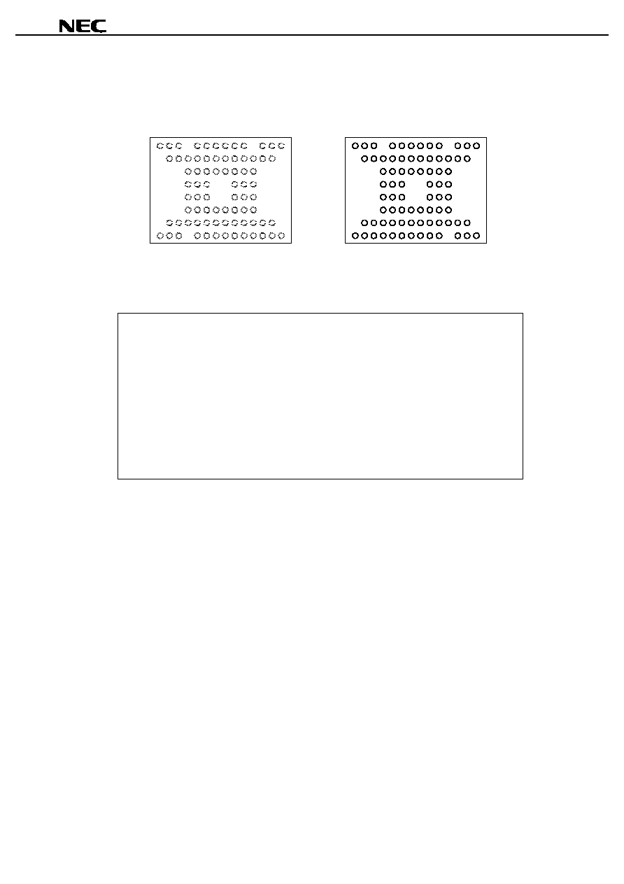
Pin Configuration
/xxx indicates active low signal.
77-pin TAPE FBGA (12
◊
◊
◊
◊
7)
Top View
V
SS
I/O9
I/O5
A7
/OE
I/O7
I/O4
I/O0
A6
A18
A11
A8
A5
I/O8
I/O12
A13
A17
SA
/CEf
I/O10
V
CC
f
/WE
V
CC
s
A16
I/O11
RY(/BY)
/RESET
A12
I/O6
I/O13
A9
A15
A19
I/O14
/CE1s
I/O15, A-1
I/O1
A1
A2
A4
A10
CIOs
I/O2
A0
A3
CE2s
A20
A14
/LB
CIOf
/WP(ACC)
/UB
I/O3
NC
NC
V
SS
Top View
Bottom View
8
7
6
5
4
3
2
1
8
7
6
5
4
3
2
1
P N M L K J H G F E D C B A
A B C D E F G H J K L M N P
A
B
C
D
E
F
G
H
J
K
L
M
N
P
NC
NC
NC
NC
NC
NC
NC
NC
NC
NC
NC
NC
NC
NC
NC
NC
NC
NC
NC
NC
NC
Common Pins
A0 - A17
: Address inputs
I/O0 - I/O15 : Data inputs / outputs
/OE
: Output Enable
/WE
: Write Enable
V
SS
: Ground
NC
Note
: No Connection
Flash Memory Pins
A18 - A20 : Address inputs
I/O15, A
-
1 : Data inputs / outputs 15 (WORD mode)
LSB address input (BYTE mode)
/CEf
: Chip Enable
RY (/BY)
: Ready (Busy) output
/RESET
: Hardware reset input
V
CC
f
: Supply Voltage
/WP(ACC) : Hardware Write Protect (Acceleration)
CIOf
: Selects 8-bit or 16-bit mode
SRAM Pins
SA
: Address input (A18 for SRAM)
/CE1s
: Chip Enable 1
CE2s
: Chip Enable 2
V
CC
s
: Supply Voltage
/LB, /UB
: Byte data select
CIOs
: Selects 8-bit or 16-bit mode
Note Some signals can be applied because this pin is not internally connected.
Remark Refer to Package Drawing for the index mark.
Data Sheet M15318EJ2V0DS
4
MC-222244A-X
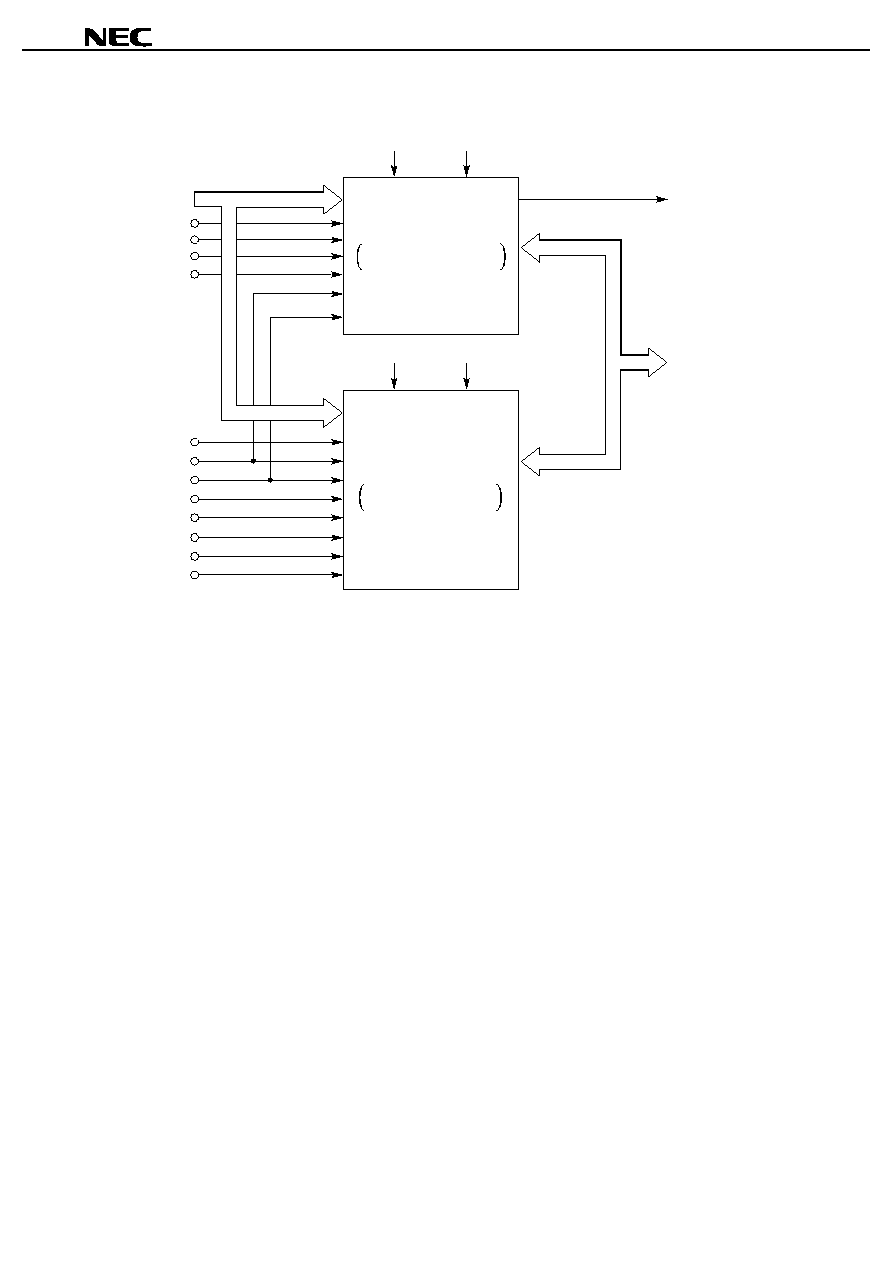
Block Diagram
32 M-bit Flash Memory
4,194,304 words by 8 bits
2,097,152 words by 16 bits
SA
/WE
/OE
/CE1s
/RESET
/CEf
I/O0 - I/O15, A-1
A0 - A20
4 M-bit SRAM
524,288 words by 8 bits
262,144 words by 16 bits
RY (/BY)
A0 - A17
A0 - A20
V
CC
f
V
SS
V
CC
s
V
SS
CE2s
/LB
/UB
CIOs
CIOf
/WP(ACC)

Data Sheet M15318EJ2V0DS
5
MC-222244A-X
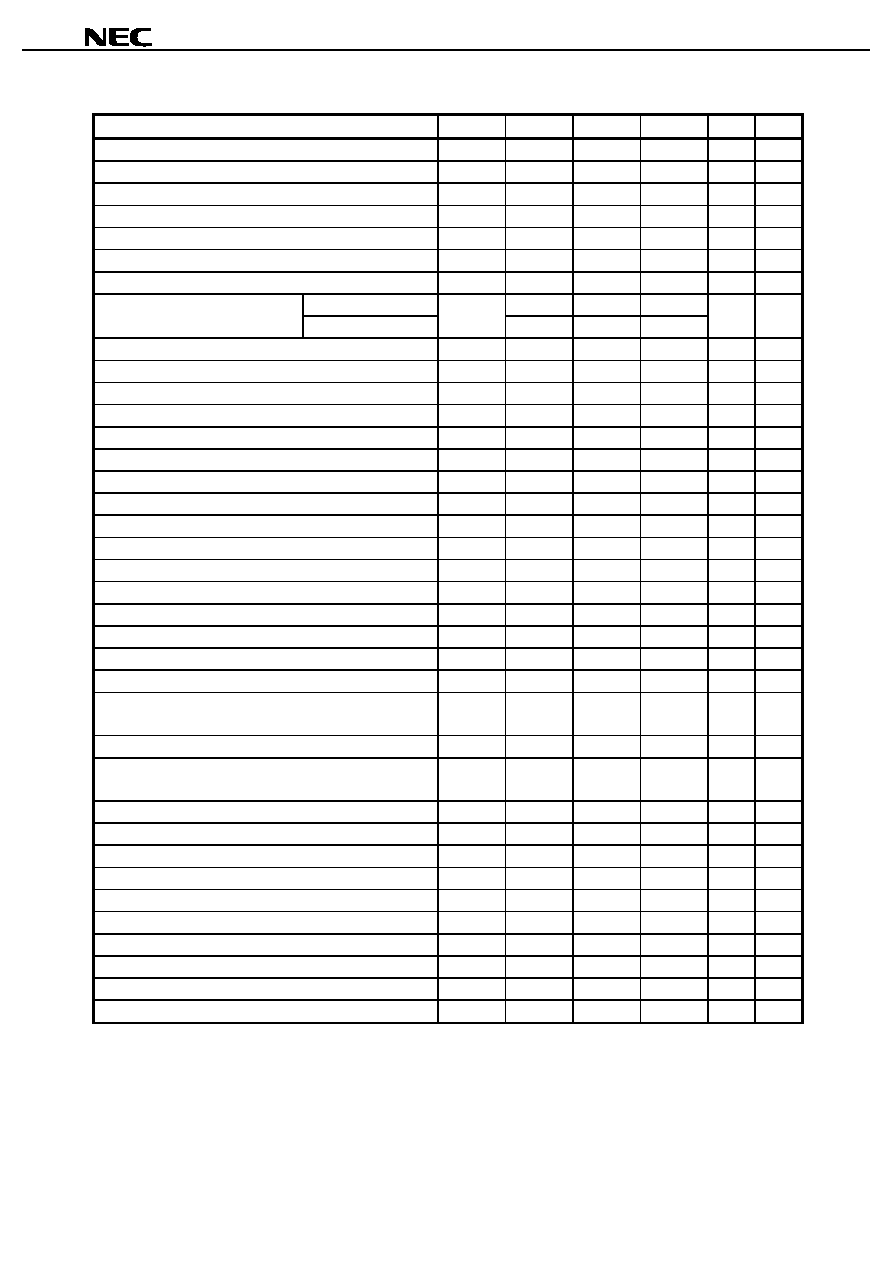
Bus Operations Table
Operation
Flash Memory
SRAM
Common
/RESET /CEf CIOf /WP(ACC) /CE1
S
CE2
S
/LB
/UB
CIOs /OE /WE I/O0 - I/O7 I/O8-I/O15
Full standby
H
H
◊
◊
H
◊
◊
◊
◊
◊
◊
Hi-Z
Hi-Z
◊
L
◊
◊
H
H
Output disable
H
L
◊
◊
L
H
◊
◊
◊
H
H
Hi-Z
Hi-Z
Read (Flash
BYTE mode
H
L
L
◊
Note 2
L
H
Data Out
Hi-Z
Memory
Note 1
) WORD mode
H
Data Out
Data Out
Write (Flash
BYTE mode
H
L
L
◊
Note 2
H
L
Data In
Hi-Z
Memory)
WORD mode
H
Data In
Data In
Temporary sector group
V
ID
◊
◊
◊
Note 2
◊
◊
Hi-Z or
Hi-Z or
unprotect
Data In/Out Data In/Out
Boot block sector protect
◊
◊
◊
L
◊
◊
◊
◊
◊
◊
◊
Hi-Z or
Data In/Out
Hi-Z or
Data In/Out
Flash Memory hardware reset
L
◊
◊
◊
◊
◊
◊
◊
◊
◊
◊
Hi-Z
Hi-Z
Read (SRAM)
BYTE mode
Note 3
L
H
◊
◊
L
L
H
Data Out
Hi-Z
WORD mode
Note 3
L
H
L
L
H
L
H
Data Out
Data Out
H
Hi-Z
H
L
Hi-Z
Data Out
Write (SRAM)
BYTE mode
Note 3
L
H
◊
◊
L
◊
L
Data In
Hi-Z
WORD mode
Note 3
L
H
L
L
H
◊
L
Data In
Data In
H
Hi-Z
H
L
Hi-Z
Data In
Caution Other operations except for indicated in this table are inhibited.
Notes 1. When /OE = V
IL
, V
IL
can be applied to /WE. When /OE = V
IH
, a write operation is started.
2. SRAM should be Standby.
3. Flash Memory should be Standby or Hardware reset.
Remarks 1. H : V
IH
, L : V
IL
,
◊
: V
IH
or V
IL
2. Sector group protection and read the product ID are using a command.
3. Refer to DUAL OPERATION FLASH MEMORY 32M BITS A SERIES Information (M14914E) for the
flash memory bus operations.
Data Sheet M15318EJ2V0DS
6
MC-222244A-X
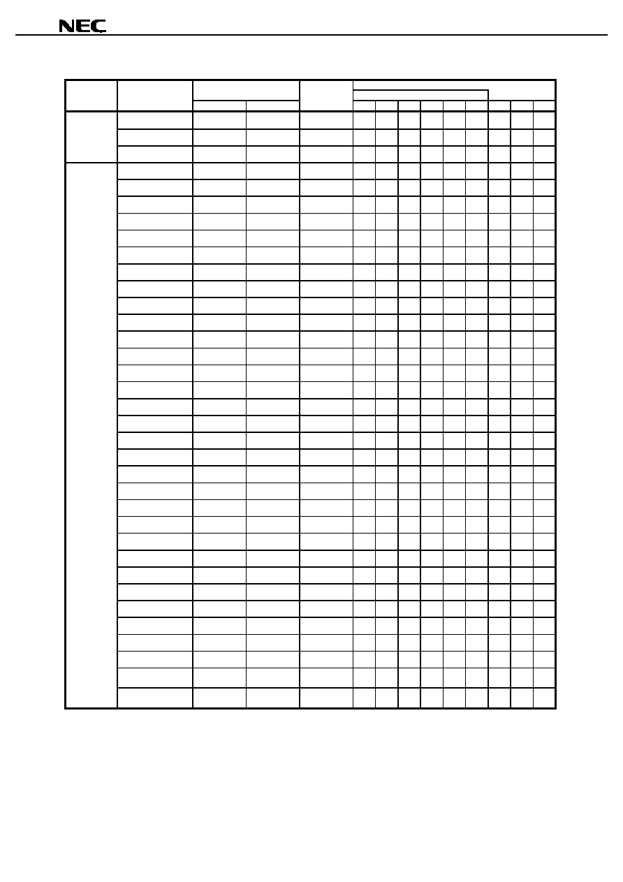
Sector Organization / Sector Address Table (Flash Memory)
Flash Memory top boot
(1/2)
Bank
Sector
Address
Sectors
Sector Address Table
Organization
Address
Bank Address Table
K bytes / K words
BYTE mode
WORD mode
A20 A19 A18 A17 A16 A15 A14 A13 A12
Bank 1
8/4
3FFFFFH
1FFFFFH
FSA70
1
1
1
1
1
1
1
1
1
3FE000H
1FF000H
8/4
3FDFFFH
1FEFFFH
FSA69
1
1
1
1
1
1
1
1
0
3FC000H
1FE000H
8/4
3FBFFFH
1FDFFFH
FSA68
1
1
1
1
1
1
1
0
1
3FA000H
1FD000H
8/4
3F9FFFH
1FCFFFH
FSA67
1
1
1
1
1
1
1
0
0
3F8000H
1FC000H
8/4
3F7FFFH
1FBFFFH
FSA66
1
1
1
1
1
1
0
1
1
3F6000H
1FB000H
8/4
3F5FFFH
1FAFFFH
FSA65
1
1
1
1
1
1
0
1
0
3F4000H
1FA000H
8/4
3F3FFFH
1F9FFFH
FSA64
1
1
1
1
1
1
0
0
1
3F2000H
1F9000H
8/4
3F1FFFH
1F8FFFH
FSA63
1
1
1
1
1
1
0
0
0
3F0000H
1F8000H
64/32
3EFFFFH
1F7FFFH
FSA62
1
1
1
1
1
0
x
x
x
3E0000H
1F0000H
64/32
3DFFFFH
1EFFFFH
FSA61
1
1
1
1
0
1
x
x
x
3D0000H
1E8000H
64/32
3CFFFFH
1E7FFFH
FSA60
1
1
1
1
0
0
x
x
x
3C0000H
1E0000H
64/32
3BFFFFH
1DFFFFH
FSA59
1
1
1
0
1
1
x
x
x
3B0000H
1D8000H
64/32
3AFFFFH
1D7FFFH
FSA58
1
1
1
0
1
0
x
x
x
3A0000H
1D0000H
64/32
39FFFFH
1CFFFFH
FSA57
1
1
1
0
0
1
x
x
x
390000H
1C8000H
64/32
38FFFFH
1C7FFFH
FSA56
1
1
1
0
0
0
x
x
x
380000H
1C0000H
64/32
37FFFFH
1BFFFFH
FSA55
1
1
0
1
1
1
x
x
x
370000H
1B8000H
64/32
36FFFFH
1B7FFFH
FSA54
1
1
0
1
1
0
x
x
x
360000H
1B0000H
64/32
35FFFFH
1AFFFFH
FSA53
1
1
0
1
0
1
x
x
x
350000H
1A8000H
64/32
34FFFFH
1A7FFFH
FSA52
1
1
0
1
0
0
x
x
x
340000H
1A0000H
64/32
33FFFFH
19FFFFH
FSA51
1
1
0
0
1
1
x
x
x
330000H
198000H
64/32
32FFFFH
197FFFH
FSA50
1
1
0
0
1
0
x
x
x
320000H
190000H
64/32
31FFFFH
18FFFFH
FSA49
1
1
0
0
0
1
x
x
x
310000H
188000H
64/32
30FFFFH
187FFFH
FSA48
1
1
0
0
0
0
x
x
x
300000H
180000H
64/32
2FFFFFH
17FFFFH
FSA47
1
0
1
1
1
1
x
x
x
2F0000H
178000H
64/32
2EFFFFH
177FFFH
FSA46
1
0
1
1
1
0
x
x
x
2E0000H
170000H
64/32
2DFFFFH
16FFFFH
FSA45
1
0
1
1
0
1
x
x
x
2D0000H
168000H
64/32
2CFFFFH
167FFFH
FSA44
1
0
1
1
0
0
x
x
x
2C0000H
160000H
64/32
2BFFFFH
15FFFFH
FSA43
1
0
1
0
1
1
x
x
x
2B0000H
158000H
64/32
2AFFFFH
157FFFH
FSA42
1
0
1
0
1
0
x
x
x
2A0000H
150000H
64/32
29FFFFH
14FFFFH
FSA41
1
0
1
0
0
1
x
x
x
290000H
148000H
64/32
28FFFFH
147FFFH
FSA40
1
0
1
0
0
0
x
x
x
280000H
140000H
64/32
27FFFFH
13FFFFH
FSA39
1
0
0
1
1
1
x
x
x
270000H
138000H
64/32
26FFFFH
137FFFH
FSA38
1
0
0
1
1
0
x
x
x
260000H
130000H
64/32
25FFFFH
12FFFFH
FSA37
1
0
0
1
0
1
x
x
x
250000H
128000H
64/32
24FFFFH
127FFFH
FSA36
1
0
0
1
0
0
x
x
x
240000H
120000H
64/32
23FFFFH
11FFFFH
FSA35
1
0
0
0
1
1
x
x
x
230000H
118000H
Data Sheet M15318EJ2V0DS
7
MC-222244A-X
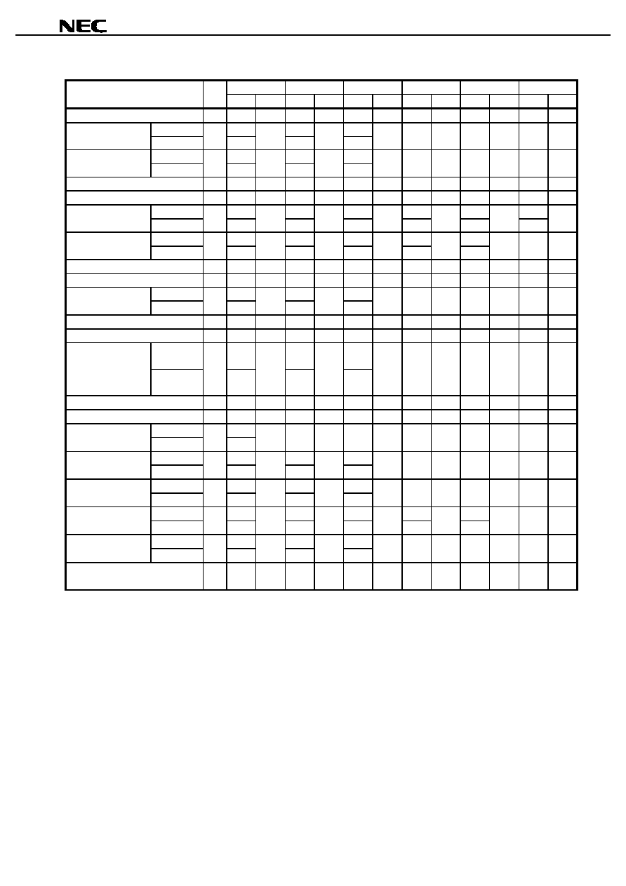
(2/2)
Bank
Sector
Address
Sectors
Sector Address Table
Organization
Address
Bank Address Table
K bytes / K words
BYTE mode
WORD mode
A20 A19 A18 A17 A16 A15 A14 A13 A12
Bank 1
64/32
22FFFFH
117FFFH
FSA34
1
0
0
0
1
0
x
x
x
220000H
110000H
64/32
21FFFFH
10FFFFH
FSA33
1
0
0
0
0
1
x
x
x
210000H
108000H
64/32
20FFFFH
107FFFH
FSA32
1
0
0
0
0
0
x
x
x
200000H
100000H
Bank 2
64/32
1FFFFFH
0FFFFFH
FSA31
0
1
1
1
1
1
x
x
x
1F0000H
0F8000H
64/32
1EFFFFH
0F7FFFH
FSA30
0
1
1
1
1
0
x
x
x
1E0000H
0F0000H
64/32
1DFFFFH
0EFFFFH
FSA29
0
1
1
1
0
1
x
x
x
1D0000H
0E8000H
64/32
1CFFFFH
0E7FFFH
FSA28
0
1
1
1
0
0
x
x
x
1C0000H
0E0000H
64/32
1BFFFFH
0DFFFFH
FSA27
0
1
1
0
1
1
x
x
x
1B0000H
0D8000H
64/32
1AFFFFH
0D7FFFH
FSA26
0
1
1
0
1
0
x
x
x
1A0000H
0D0000H
64/32
19FFFFH
0CFFFFH
FSA25
0
1
1
0
0
1
x
x
x
190000H
0C8000H
64/32
18FFFFH
0C7FFFH
FSA24
0
1
1
0
0
0
x
x
x
180000H
0C0000H
64/32
17FFFFH
0BFFFFH
FSA23
0
1
0
1
1
1
x
x
x
170000H
0B8000H
64/32
16FFFFH
0B7FFFH
FSA22
0
1
0
1
1
0
x
x
x
160000H
0B0000H
64/32
15FFFFH
0AFFFFH
FSA21
0
1
0
1
0
1
x
x
x
150000H
0A8000H
64/32
14FFFFH
0A7FFFH
FSA20
0
1
0
1
0
0
x
x
x
140000H
0A0000H
64/32
13FFFFH
09FFFFH
FSA19
0
1
0
0
1
1
x
x
x
130000H
098000H
64/32
12FFFFH
097FFFH
FSA18
0
1
0
0
1
0
x
x
x
120000H
090000H
64/32
11FFFFH
08FFFFH
FSA17
0
1
0
0
0
1
x
x
x
110000H
088000H
64/32
10FFFFH
087FFFH
FSA16
0
1
0
0
0
0
x
x
x
100000H
080000H
64/32
0FFFFFH
07FFFFH
FSA15
0
0
1
1
1
1
x
x
x
0F0000H
078000H
64/32
0EFFFFH
077FFFH
FSA14
0
0
1
1
1
0
x
x
x
0E0000H
070000H
64/32
0DFFFFH
06FFFFH
FSA13
0
0
1
1
0
1
x
x
x
0D0000H
068000H
64/32
0CFFFFH
067FFFH
FSA12
0
0
1
1
0
0
x
x
x
0C0000H
060000H
64/32
0BFFFFH
05FFFFH
FSA11
0
0
1
0
1
1
x
x
x
0B0000H
058000H
64/32
0AFFFFH
057FFFH
FSA10
0
0
1
0
1
0
x
x
x
0A0000H
050000H
64/32
09FFFFH
04FFFFH
FSA9
0
0
1
0
0
1
x
x
x
090000H
048000H
64/32
08FFFFH
047FFFH
FSA8
0
0
1
0
0
0
x
x
x
080000H
040000H
64/32
07FFFFH
03FFFFH
FSA7
0
0
0
1
1
1
x
x
x
070000H
038000H
64/32
06FFFFH
037FFFH
FSA6
0
0
0
1
1
0
x
x
x
060000H
030000H
64/32
05FFFFH
02FFFFH
FSA5
0
0
0
1
0
1
x
x
x
050000H
028000H
64/32
04FFFFH
027FFFH
FSA4
0
0
0
1
0
0
x
x
x
040000H
020000H
64/32
03FFFFH
01FFFFH
FSA3
0
0
0
0
1
1
x
x
x
030000H
018000H
64/32
02FFFFH
017FFFH
FSA2
0
0
0
0
1
0
x
x
x
020000H
010000H
64/32
01FFFFH
00FFFFH
FSA1
0
0
0
0
0
1
x
x
x
010000H
008000H
64/32
00FFFFH
007FFFH
FSA0
0
0
0
0
0
0
x
x
x
000000H
000000H

Data Sheet M15318EJ2V0DS
8
MC-222244A-X
Sector Group Address Table (Flash Memory)
Sector group
A20
A19
A18
A17
A16
A15
A14
A13
A12
Size
Sector
SGA0
0
0
0
0
0
0
◊
◊
◊
64 KB (1 Sector)
FSA0
SGA1
0
0
0
0
0
1
◊
◊
◊
192 KB (3 Sectors)
FSA1≠FSA3
1
0
1
1
SGA2
0
0
0
1
◊
◊
◊
◊
◊
256 KB (4 Sectors)
FSA4≠FSA7
SGA3
0
0
1
0
◊
◊
◊
◊
◊
256 KB (4 Sectors)
FSA8≠FSA11
SGA4
0
0
1
1
◊
◊
◊
◊
◊
256 KB (4 Sectors)
FSA12≠FSA15
SGA5
0
1
0
0
◊
◊
◊
◊
◊
256 KB (4 Sectors)
FSA16≠FSA19
SGA6
0
1
0
1
◊
◊
◊
◊
◊
256 KB (4 Sectors)
FSA20≠FSA23
SGA7
0
1
1
0
◊
◊
◊
◊
◊
256 KB (4 Sectors)
FSA24≠FSA27
SGA8
0
1
1
1
◊
◊
◊
◊
◊
256 KB (4 Sectors)
FSA28≠FSA31
SGA9
1
0
0
0
◊
◊
◊
◊
◊
256 KB (4 Sectors)
FSA32≠FSA35
SGA10
1
0
0
1
◊
◊
◊
◊
◊
256 KB (4 Sectors)
FSA36≠FSA39
SGA11
1
0
1
0
◊
◊
◊
◊
◊
256 KB (4 Sectors)
FSA40≠FSA43
SGA12
1
0
1
1
◊
◊
◊
◊
◊
256 KB (4 Sectors)
FSA44≠FSA47
SGA13
1
1
0
0
◊
◊
◊
◊
◊
256 KB (4 Sectors)
FSA48≠FSA51
SGA14
1
1
0
1
◊
◊
◊
◊
◊
256 KB (4 Sectors)
FSA52≠FSA55
SGA15
1
1
1
0
◊
◊
◊
◊
◊
256 KB (4 Sectors)
FSA56≠FSA59
SGA16
1
1
1
1
0
0
◊
◊
◊
192 KB (3 Sectors)
FSA60≠FSA62
0
1
1
0
SGA17
1
1
1
1
1
1
0
0
0
8 KB (1 Sector)
FSA63
SGA18
1
1
1
1
1
1
0
0
1
8 KB (1 Sector)
FSA64
SGA19
1
1
1
1
1
1
0
1
0
8 KB (1 Sector)
FSA65
SGA20
1
1
1
1
1
1
0
1
1
8 KB (1 Sector)
FSA66
SGA21
1
1
1
1
1
1
1
0
0
8 KB (1 Sector)
FSA67
SGA22
1
1
1
1
1
1
1
0
1
8 KB (1 Sector)
FSA68
SGA23
1
1
1
1
1
1
1
1
0
8 KB (1 Sector)
FSA69
SGA24
1
1
1
1
1
1
1
1
1
8 KB (1 Sector)
FSA70
Remark
◊
: V
IH
or V
IL
Data Sheet M15318EJ2V0DS
9
MC-222244A-X
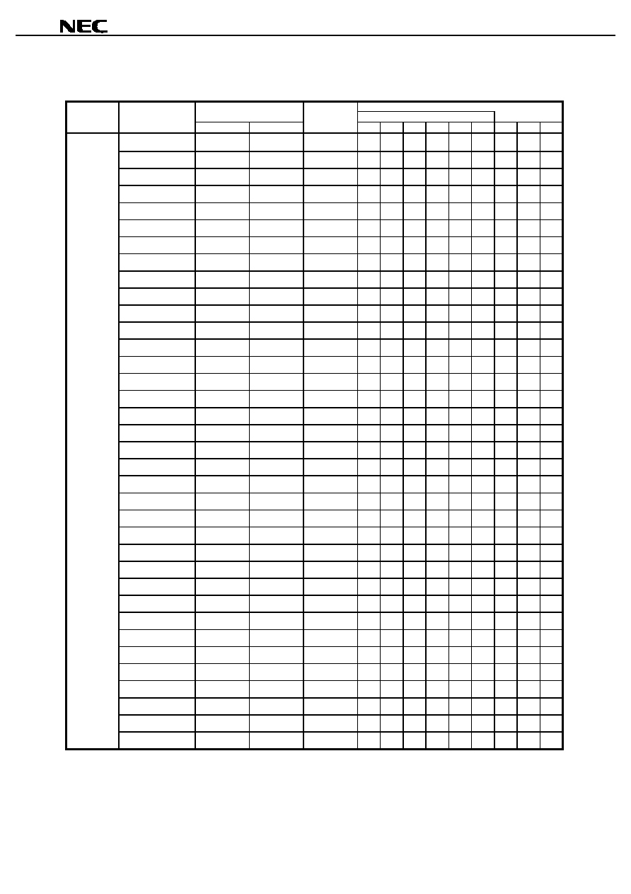
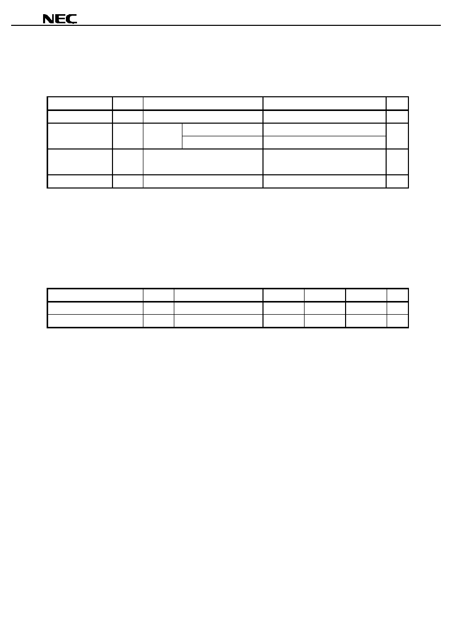
Command Sequence (Flash Memory)
Command sequence
Bus
1st bus Cycle
2nd bus Cycle
3rd bus Cycle
4th bus Cycle
5th bus Cycle
6th bus Cycle
Cycle Address Data
Address Data Address Data
Address Data Address Data
Address Data
Read / Reset
Note1
1
◊◊◊
H
F0H
RA
RD
≠
≠
≠
≠
≠
≠
≠
≠
Read / Reset
Note1
BYTE mode
3
AAAH
AAH
555H
55H
AAAH
F0H
RA
RD
≠
≠
≠
≠
WORD mode
555H
2AAH
555H
Program
BYTE mode
4
AAAH
AAH
555H
55H
AAAH
A0H
PA
PD
≠
≠
≠
≠
WORD mode
555H
2AAH
555H
Program Suspend
Note 2
1
BA
B0H
≠
≠
≠
≠
≠
≠
≠
≠
≠
≠
Program Resume
Note 3
1
BA
30H
≠
≠
≠
≠
≠
≠
≠
≠
≠
≠
Chip Erase
BYTE mode
6
AAAH
AAH
555H
55H
AAAH
80H
AAAH
AAH
555H
55H
AAAH
10H
WORD mode
555H
2AAH
555H
555H
2AAH
555H
Sector Erase
BYTE mode
6
AAAH
AAH
555H
55H
AAAH
80H
AAAH
AAH
555H
55H
FSA
30H
WORD mode
555H
2AAH
555H
555H
2AAH
Sector Erase Suspend
Note 4
1
BA
B0H
≠
≠
≠
≠
≠
≠
≠
≠
≠
≠
Sector Erase Resume
Note 5
1
BA
30H
≠
≠
≠
≠
≠
≠
≠
≠
≠
≠
Unlock Bypass Set
BYTE mode
3
AAAH
AAH
555H
55H
AAAH
20H
≠
≠
≠
≠
≠
≠
WORD mode
555H
2AAH
555H
Unlock Bypass Program
Note 6
2
◊◊◊
H
A0H
PA
PD
≠
≠
≠
≠
≠
≠
≠
≠
Unlock Bypass Reset
Note 6
2
BA
90H
◊◊◊
H 00H
Note11
≠
≠
≠
≠
≠
≠
≠
≠
Product ID
BYTE mode
3
AAAH
AAH
555H
55H
(BA)
90H
IA
ID
≠
≠
≠
≠
AAAH
WORD mode
555H
2AAH
(BA)
555H
Sector Group Protection
Note 7
4
◊◊◊
H
60H
SPA
60H
SPA
40H
SPA
SD
≠
≠
≠
≠
Sector Group Unprotect
Note 8
4
◊◊◊
H
60H
SUA
60H
SUA
40H
SUA
SD
≠
≠
≠
≠
Query
Note 9
BYTE mode
1
AAH
98H
≠
≠
≠
≠
≠
≠
≠
≠
≠
≠
WORD mode
55H
Extra One Time Protect
BYTE mode
3
AAAH
AAH
555H
55H
AAAH
88H
≠
≠
≠
≠
≠
≠
Sector Entry
WORD mode
555H
2AAH
555H
Extra One Time Protect
BYTE mode
4
AAAH
AAH
555H
55H
AAAH
A0H
PA
PD
≠
≠
≠
≠
Sector Program
Note 10
WORD mode
555H
2AAH
555H
Extra One Time Protect
BYTE mode
6
AAAH
AAH
555H
55H
AAAH
80H
AAAH
AAH
555H
55H
EOTPSA 30H
Sector Erase
Note 10
WORD mode
555H
2AAH
555H
555H
2AAH
Extra One Time Protect
BYTE mode
4
AAAH
AAH
555H
55H
AAAH
90H
xxxH
00H
≠
≠
≠
≠
Sector Reset
Note 10
WORD mode
555H
2AAH
555H
Extra One Time Protect Sector
4
◊◊◊
H
60H
EOTPSA
60H
EOTPSA
40H
EOTPSA
SD
≠
≠
≠
≠
Protection
Note 10

Data Sheet M15318EJ2V0DS
10
MC-222244A-X
Notes 1. Both these read / reset commands reset the device to the read mode.
2. Programming is suspended if B0H is input to the bank address being programmed to in a program
operation.
3. Programming is resumed if 30H is input to the bank address being suspended to in a program-suspend
operation.
4. Erasure is suspended if B0H is input to the bank address being erased in a sector erase operation.
5. Erasure is resumed if 30H is input to the bank address being suspended in a sector-erase-suspend
operation.
6. Valid only in the unlock bypass mode.
7. Valid only when /RESET = V
ID
(except in the Extra One Time Protect Sector mode).
8. The command sequence that protects a sector group is excluded.
9. Only A0 to A6 are valid as an address.
10. Valid only in the Extra One Time Protect Sector mode.
11. This command can be used even if this data is F0H.
Remarks 1. Specify address 555H or 2AAH (A10 to A0) in the WORD mode, and AAAH or 555H (A10 to A0, A-1) in
the BYTE mode.
2. RA : Read address
RD : Read data
IA : Address input
xx00H (to read the manufacturer code)
xx02H (to read the device code in the BYTE mode)
xx01H (to read the device code in the WORD mode)
ID : Code output. Refer to the Product ID code (Manufacturer code / Device code) (Flash Memory).
PA : Program address
PD : Program data
FSA: Erase sector address. The sector to be erased is selected by the combination of this address.
Refer to the Sector Organization / Sector Address Table (Flash Memory).
BA : Bank address. Refer to the Sector Organization / Sector Address Table (Flash Memory).
SPA : Sector group address to be protected. Set sector group address (SGA) and (A6, A1, A0) =
(V
IL
, V
IH
, V
IL
). For the sector group address, refer to the Sector Group Address Table (Flash
Memory).
SUA : Unprotect sector group address. Set sector group address (SGA) and (A6, A1, A0) =
(V
IH
, V
IH
, V
IL
). For the sector group address, refer to the Sector Group Address Table (Flash
Memory).
SD : Data for verifying whether sector groups read from the address specified by SPA, SUA, and
EOTPSA are protected.
EOTPSA : Extra One Time Protect Sector area addresses.
BYTE mode : 3F0000H to 3FFFFFH, WORD mode : 1F8000H to 1FFFFFH
3. The sector group address is don't care except when a program / erase address or read address are
selected.
4. For the operation of the bus, refer to Bus Operations Table.
5.
◊
of address bit indicates V
IH
or V
IL
.
6. Refer to DUAL OPERATION FLASH MEMORY 32M BITS A SERIES Information (M14914E) for the
flash memory commands.

Data Sheet M15318EJ2V0DS
11
MC-222244A-X
Product ID Code (Manufacturer Code / Device Code) (Flash Memory)
Product ID Code
Address inputs
Output
A6
A1
A0
Hex
Manufacturer Code
L
L
L
10H
Device code
L
L
H
5CH (BYTE mode),
225CH (WORD mode)
Product ID Code
Code outputs
I/O
15
I/O
14
I/O
13
I/O
12
I/O
11
I/O
10
I/O
9
I/O
8
I/O
7
I/O
6
I/O
5
I/O
4
I/O
3
I/O
2
I/O
1
I/O
0
Hex
Manufacturer Code
0
0
0
0
0
0
0
0
0
0
0
1
0
0
0
0
10H
Device code BYTE mode
A-1
x
x
x
x
x
x
x
0
1
0
1
1
1
0
0
5CH
WORD mode
0
0
1
0
0
0
1
0
0
1
0
1
1
1
0
0
225CH
Remark H : V
IH
, L : V
IL
, x : Hi-Z
Hardware Sequence Flags, Hardware Data Protection (Flash Memory)
Refer to DUAL OPERATION FLASH MEMORY 32M BITS A SERIES Information (M14914E).
Data Sheet M15318EJ2V0DS
12
MC-222244A-X
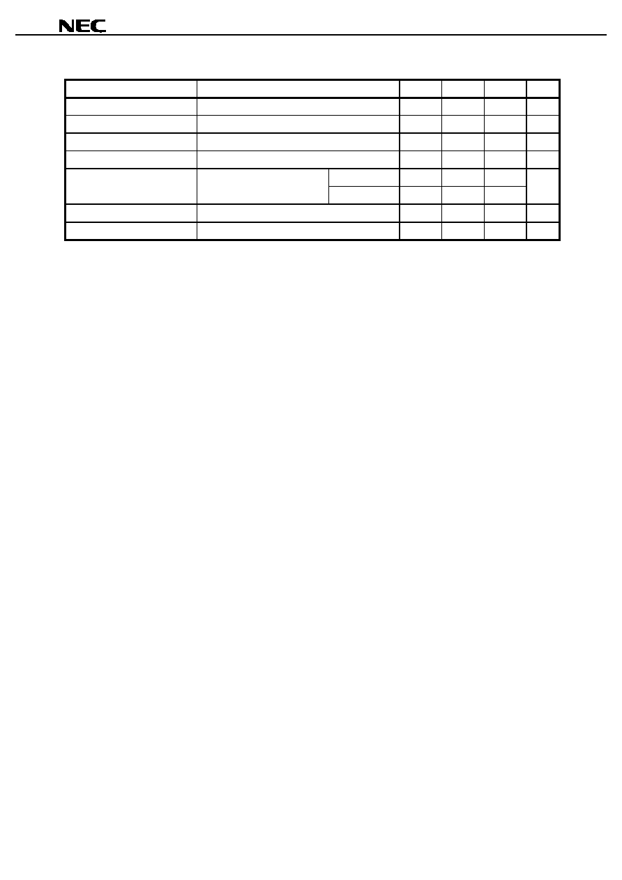
Electrical Specifications
Before turning on power, input V
SS
±
0.2 V to the /RESET pin until V
CC
f
V
CC
f (MIN.).
Absolute Maximum Ratings
Parameter
Symbol
Condition
Rating
Unit
Supply voltage
V
CC
f, V
CC
s with respect to V
SS
≠0.5 to +4.0
V
Input / Output voltage
V
T
with respect /WP(ACC), /RESET
≠0.5
Note 1
to +13.0
V
to V
SS
except /WP(ACC), /RESET
≠0.5
Note 1
to V
CC
f, V
CC
s + 0.4 (4.0 V MAX.)
Note 2
Ambient operation
T
A
≠25 to +85
∞
C
temperature
Storage temperature
T
stg
≠55 to +125
∞
C
Notes 1. ≠2.0 V (MIN.) (pulse width
20 ns)
2. V
CC
f, V
CC
s + 0.5 V (MAX.) (pulse width
20 ns)
Caution Exposing the device to stress above those listed in Absolute Maximum Rating could cause
permanent damage. The device is not meant to be operated under conditions outside the limits
described in the operational section of this specification. Exposure to Absolute Maximum Rating
conditions for extended periods may affect device reliability.
Recommended Operating Conditions
Parameter
Symbol
Condition
MIN.
TYP.
MAX.
Unit
Supply voltage
V
CC
f, V
CC
s
2.7
3.6
V
Ambient operation temperature
T
A
≠25
+85
∞
C

Data Sheet M15318EJ2V0DS
13
MC-222244A-X
DC Characteristics (Recommended Operating Conditions Unless Otherwise Noted)
Common
Parameter
Symbol
Test condition
MIN.
TYP.
MAX.
Unit
High level input voltage
V
IH
2.4
V
CC
f, V
CC
s + 0.3
V
Low level input voltage
V
IL
-
0.3
+0.5
V
High level output voltage
V
OH
I
OH
=
-
500
µ
A, V
CC
f = V
CC
f (MIN.),
2.4
V
V
CC
s = V
CC
s (MIN.)
Low level output voltage
V
OL
I
OL
= +1.0 mA, V
CC
f = V
CC
f (MIN.),
0.4
V
V
CC
s = V
CC
s (MIN.)
Input leakage current
I
LI
-
1.0
+1.0
µ
A
Output leakage current
I
LO
-
1.0
+1.0
µ
A
Flash Memory
Parameter
Symbol
Test condition
MIN.
TYP.
MAX.
Unit
Power
Read
BYTE mode
I
CC1
f
V
CC
f = V
CC
f (MAX.),
t
CYCLE
= 5 MHz
10
16
mA
supply
/CEf = V
IL
, /OE = V
IH
t
CYCLE
= 1 MHz
2
4
current
WORD mode
t
CYCLE
= 5 MHz
10
16
t
CYCLE
= 1 MHz
2
4
Program, Erase
I
CC2
f
V
CC
f = V
CC
f (MAX.), /CEf = V
IL
, /OE = V
IH
15
30
mA
Standby
I
CC3
f
V
CC
f = V
CC
f (MAX.), /CEf = /RESET =
0.2
5
µ
A
/WP(ACC) = V
CC
f
±
0.3 V, /OE = V
IL
Standby / Reset
I
CC4
f
V
CC
f = V
CC
f (MAX.), /RESET = V
SS
±
0.2 V
0.2
5
µ
A
Automatic sleep mode
I
CC5
f
V
IH
= V
CC
f
±
0.2 V, V
IL
= V
SS
±
0.2 V
0.2
5
µ
A
Read during programming
I
CC6
f
V
IH
= V
CC
f
±
0.2 V, V
IL
= V
SS
±
0.2 V
21
45
mA
Read during erasing
I
CC7
f
V
IH
= V
CC
f
±
0.2 V, V
IL
= V
SS
±
0.2 V
21
45
mA
Programming
I
CC8
f
/CEf = V
IL
, /OE = V
IH
,
17
35
mA
during suspend
Automatic programming during suspend
Accelerated
I
ACC
/WP (ACC) pin
5
10
mA
programming
V
CC
f
15
30
/RESET high level input voltage
V
ID
High Voltage is applied
11.5
12.5
V
Accelerated programming voltage
V
ACC
High Voltage is applied
8.5
9.5
V
Low V
CC
f lock-out voltage
Note
V
LKO
1.7
V
Note When V
CC
f is equal to or lower than V
LKO
, the device ignores all write cycles. Refer to Refer to DUAL
OPERATION FLASH MEMORY 32M BITS A SERIES Information (M14914E).
SRAM
Parameter
Symbol
Test condition
MIN.
TYP.
MAX.
Unit
Power supply current
I
CC1S
/CE1s = V
IL
, CE2s = V
IH
, Minimum cycle time, I
I/O
= 0 mA
≠
40
mA
/CE1s = V
IL
, CE2s = V
IH
, I
I/O
= 0 mA, Cycle time =
≠
10
I
CC2S
/CE1s
0.2 V, CE2s
V
CC
s ≠ 0.2 V, Cycle time = 1
µ
s,
≠
8
I
I/O
= 0 mA, V
IL
0.2 V, V
IH
V
CC
s ≠ 0.2 V
Standby supply current
I
SB1S
/CE1s = V
IH
or CE2s = V
IL
or /LB = /UB = V
IH
≠
0.6
mA
I
SB2S
/CE1s
V
CC
s
-
0.2 V, CE2s
V
CC
s
-
0.2 V
0.5
7
µ
A
CE2s
0.2 V
0.5
7
/LB = /UB
V
CC
s
-
0.2 V, /CE1s
0.2 V, CE2s
V
CC
s
-
0.2 V
0.5
7
Data Sheet M15318EJ2V0DS
14
MC-222244A-X
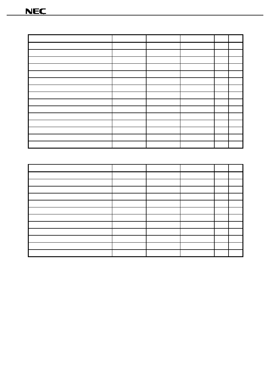
AC Characteristics (Recommended Operating Conditions Unless Otherwise Noted)
AC Test Conditions
Flash Memory
Input Waveform (Rise and Fall Time
5 ns)
Test Points
V
SS
3.0 V
1.5 V
1.5 V
Output Waveform
Test Points
1.5 V
1.5 V
Output Load
1 TTL + 30 pF
SRAM
Input Waveform (Rise and Fall Time
5 ns)
Test points
V
CC
s x 0.9 V
V
CC
s x 0.1 V
V
CC
s / 2 V
V
CC
s / 2 V
Output Waveform
Test points
V
CC
s / 2 V
V
CC
s / 2 V
Output Load
1 TTL + 30 pF
/CEf, /CE1s, CE2s Timing
Parameter
Symbol
Test Condition
MIN.
TYP.
MAX.
Unit
Notes
/CEf, /CE1s, CE2s recover time
t
CCR
0
ns

Data Sheet M15318EJ2V0DS
15
MC-222244A-X
Read Cycle (Flash Memory)
Parameter
Symbol
Test Condition
MIN.
TYP.
MAX.
Unit
Notes
Read cycle time
t
RC
85
ns
Address access time
t
ACC
/CEf = /OE = V
IL
85
ns
/CEf access time
t
CEf
/OE = V
IL
85
ns
/OE access time
t
OE
/CEf = V
IL
40
ns
Output disable time
t
DF
/OE = V
IL
or /CEf = V
IL
30
ns
Output hold time
t
OH
0
ns
/RESET pulse width
t
RP
500
ns
/RESET hold time before read
t
RH
50
ns
/RESET low to read mode
t
READY
20
µ
s
/CEf low to CIOf low, high
t
ELFL
/t
ELFH
5
ns
CIOf low output disable time
t
FLQZ
30
ns
CIOf high access time
t
FHQV
85
ns
Remark t
DF
is the time from inactivation of /CEf or /OE to Hi-Z state output.
Data Sheet M15318EJ2V0DS
16
MC-222244A-X
Write Cycle (Erase / Program) (Flash Memory)
Parameter
Symbol
MIN.
TYP.
MAX.
Unit
Notes
Write cycle time
t
WC
85
ns
Address setup time (/WE to address)
t
AS
0
ns
Address setup time (/CEf to address)
t
AS
0
ns
Address hold time (/WE to address)
t
AH
45
ns
Address hold time (/CEf to address)
t
AH
45
ns
Input data setup time
t
DS
35
ns
Input data hold time
t
DH
0
ns
/OE hold time
Read
t
OEH
0
ns
Toggle bit, Data polling
10
Read recovery time before write (/OE to /CEf)
t
GHEL
0
ns
Read recovery time before write (/OE to /WE)
t
GHWL
0
ns
/WE setup time (/CEf to /WE)
t
WS
0
ns
/CEf setup time (/WE to /CEf)
t
CS
0
ns
/WE hold time (/CEf to /WE)
t
WH
0
ns
/CEf hold time (/WE to /CEf)
t
CH
0
ns
Write pulse width
t
WP
35
ns
/CEf pulse width
t
CP
35
ns
Write pulse width high
t
WPH
30
ns
/CEf pulse width high
t
CPH
30
ns
Byte programming operation time
t
BPG
9
200
µ
s
Word programming operation time
t
WPG
11
200
µ
s
Sector erase operation time
t
SER
0.7
5
s
1
V
CC
f setup time
t
VCS
50
µ
s
RY (/BY) recovery time
t
RB
0
ns
/RESET pulse width
t
RP
500
ns
/RESET high-voltage (V
ID
) hold time from high of RY(/BY)
t
RRB
20
µ
s
when sector group is temporarily unprotect
/RESET hold time
t
RH
50
ns
From completion of automatic program / erase to data
t
EOE
85
ns
output time
RY (/BY) delay time from valid program or erase operation
t
BUSY
90
ns
Address setup time to /OE low in toggle bit
t
ASO
15
ns
Address hold time to /CEf or /OE high in toggle bit
t
AHT
0
ns
/CEf pulse width high for toggle bit
t
CEPH
20
ns
/OE pulse width high for toggle bit
t
OEPH
20
ns
Voltage transition time
t
VLHT
4
µ
s
2
Rise time to V
ID
(/RESET)
t
VIDR
500
ns
3
Rise time to V
ACC
(/WP(ACC))
t
VACCR
500
ns
2
Erase timeout time
t
TOW
50
µ
s
4
Erase suspend transition time
t
SPD
20
µ
s
4
Notes 1. The preprogramming time prior to the erase operation is not included.
2. Sector group protection and accelerated mode only
3. Sector group protection only.
4. Table only.
Data Sheet M15318EJ2V0DS
17
MC-222244A-X
Write operation (Erase / Program) Performance (Flash Memory)
Parameter
Description
MIN.
TYP.
MAX.
Unit
Sector erase time
Excludes programming time prior to erasure
0.7
5
s
Chip erase time
Excludes programming time prior to erasure
50
s
Byte programming time
Excludes system-level overhead
9
200
µ
s
Word programming time
Excludes system-level overhead
11
200
µ
s
Chip programming time
Excludes system-level overhead
BYTE mode
40
s
WORD mode
25
Accelerated programming time
Excludes system-level overhead
7
150
µ
s
Erase / Program cycle
100,000
cycles
Data Sheet M15318EJ2V0DS
18
MC-222244A-X
Read Cycle (SRAM)
Parameter
Symbol
MIN.
MAX.
Unit
Notes
Read cycle time
t
RC
70
ns
Address access time
t
AA
70
ns
/CE1s access time
t
CO1
70
ns
CE2s access time
t
CO2
70
ns
/OE to output valid
t
OE
35
ns
/LB, /UB to output valid
t
BA
70
ns
Output hold from address change
t
OH
10
ns
/CE1s to output in Low-Z
t
LZ1
10
ns
CE2s to output in Low-Z
t
LZ2
10
ns
/OE to output in Low-Z
t
OLZ
0
ns
/LB, /UB to output in Low-Z
t
BLZ
10
ns
/CE1s to output in Hi-Z
t
HZ1
25
ns
CE2s to output in Hi-Z
t
HZ2
25
ns
/OE to output in Hi-Z
t
OHZ
25
ns
/LB, /UB to output in Hi-Z
t
BHZ
25
ns
Write Cycle (SRAM)
Parameter
Symbol
MIN.
MAX.
Unit
Notes
Write cycle time
t
WC
70
ns
/CE1s to end of write
t
CW1
55
ns
CE2s to end of write
t
CW2
55
ns
/LB, /UB to end of write
t
BW
55
ns
Address valid to end of write
t
AW
55
ns
Address setup time
t
AS
0
ns
Write pulse width
t
WP
45
ns
Write recovery time
t
WR
0
ns
Data valid to end of write
t
DW
30
ns
Data hold time
t
DH
0
ns
/WE to output in Hi-Z
t
WHZ
25
ns
Output active from end of write
t
OW
5
ns

Data Sheet M15318EJ2V0DS
19
MC-222244A-X
Low V
CC
Data Retention Characteristics (SRAM)
Parameter
Symbol
Test Condition
MIN.
TYP.
MAX.
Unit
Data retention supply voltage
V
CCDR1
/CE1s
V
CC
s
-
0.2 V, CE2s
V
CC
s
-
0.2 V
1.0
3.6
V
V
CCDR2
CE2s
0.2 V
1.0
3.6
V
CCDR3
/LB = /UB
V
CC
s
-
0.2 V,
1.0
3.6
/CE1s
0.2 V, CE2s
V
CC
s
-
0.2 V
Data retention supply current
I
CCDR1
V
CC
s = 1.5 V, /CE1s
V
CC
s
-
0.2 V,
0.3
3
µ
A
CE2s
V
CC
s
-
0.2 V
I
CCDR2
V
CC
s = 1.5 V, CE2s
0.2 V
0.3
3
I
CCDR3
V
CC
s = 1.5 V, /LB = /UB
V
CC
s
-
0.2 V,
0.3
3
/CE1s
0.2 V, CE2s
V
CC
s
-
0.2 V
Chip deselection to data retention mode
t
CDR
0
ns
Operation recovery time
t
R
t
RC
Note
ns
Note t
RC
: Read cycle time

Data Sheet M15318EJ2V0DS
20
MC-222244A-X
Figure 1. Alternating SRAM to Flash Memory Timing Chart
/CEf (Input)
/CE1s (Input)
CE2s (Input)
t
CCR
t
CCR
t
CCR
t
CCR
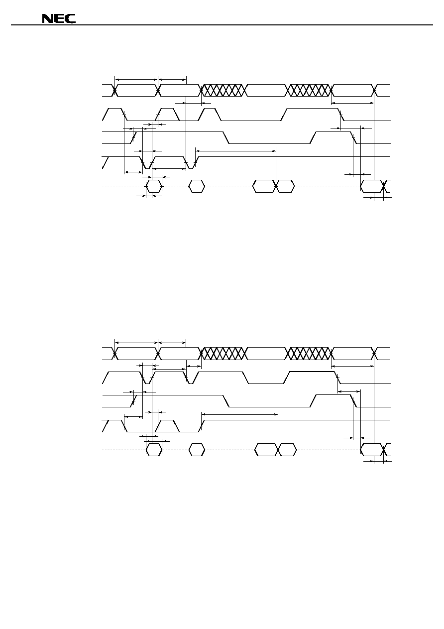
Figure 2. Read Cycle Timing Chart 1 (Flash Memory)
Address (Input)
/CEf (Input)
/OE (Input)
/WE (Input)
Hi-Z
Data out
t
OEH
t
OH
t
OE
t
CEf
t
RC
t
ACC
t
DF
Hi-Z
I/O (Output)
Figure 3. Read Cycle Timing Chart 2 (Flash Memory)
Address (Input)
/RESET (Input)
t
ACC
Hi-Z
Data out
Hi-Z
I/O (Output)
t
RC
/CEf (Input)
t
RH
t
RP
t
OH
t
CEf
t
READY
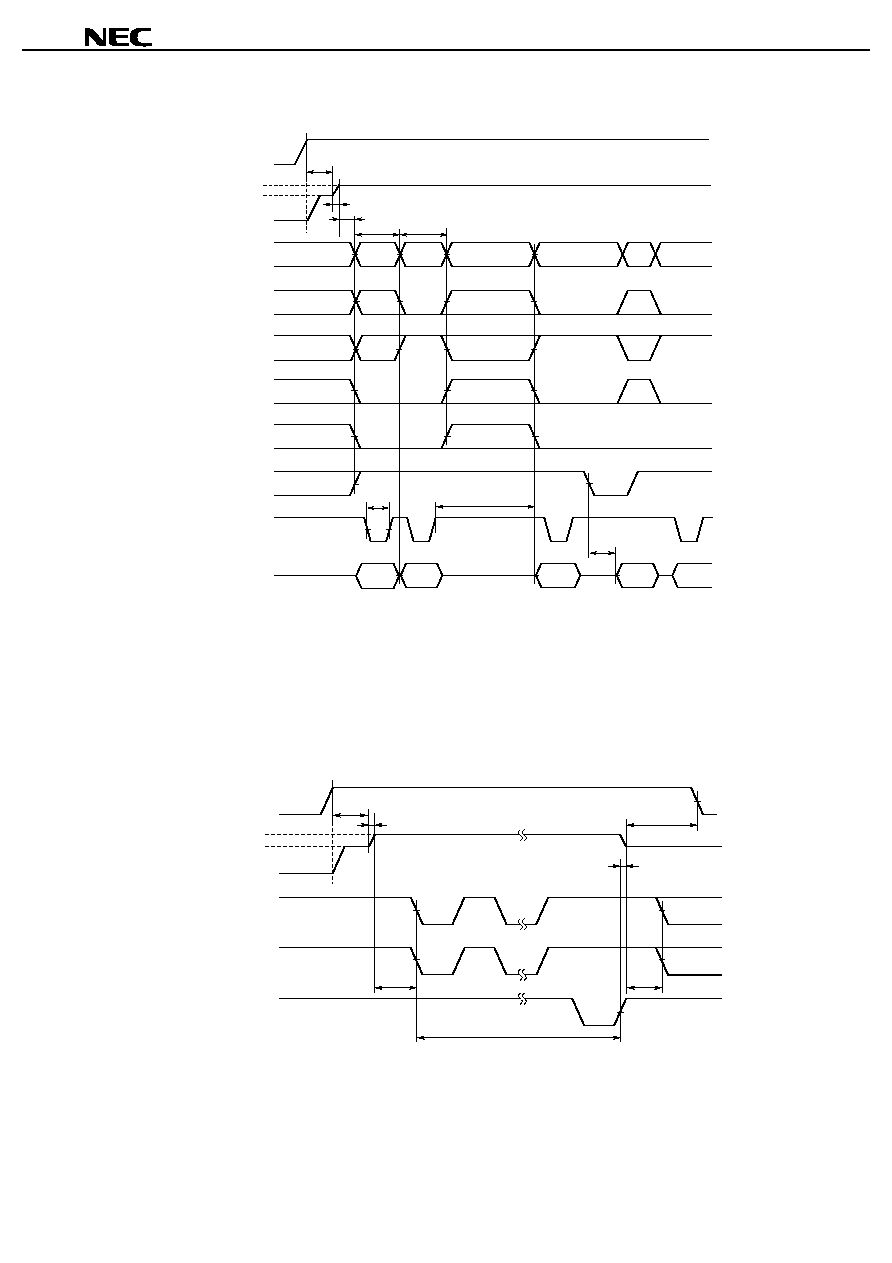
Data Sheet M15318EJ2V0DS
21
MC-222244A-X
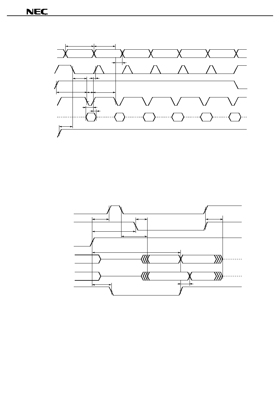
Figure 4. Sector Group Protection Timing Chart (Flash Memory)
SGAx
SGAx
Address (Input)
A0 (Input)
A1 (Input)
A6 (Input)
/CEf (Input)
/RESET (Input)
V
CC
f
/OE (Input)
/WE (Input)
I/O (Input/Output)
t
WC
t
VCS
t
VLHT
t
VIDR
t
WC
t
OE
TIMEOUT
t
WP
SGAy
60H
60H
40H
01H
Note
60H
V
ID
V
IH
Note The sector group protection verification result is output.
01H : The sector group is protected.
00H : The sector group is not protected.
Figure 5. Temporary Sector Group Unprotect Timing Chart (Flash Memory)
/RESET (Input)
V
CC
f
/WE (Input)
/CEf (Input)
RY (/BY) (Output)
V
ID
V
IH
t
VLHT
t
VCS
t
VIDR
t
RRB
t
VLHT
t
VLHT
(Program or erase command sequence)
Period during which
protection is canceled

Data Sheet M15318EJ2V0DS
22
MC-222244A-X
Figure 6. Accelerated Mode Timing Chart (Flash Memory)
/WP (ACC) (Input)
V
CC
f
/WE (Input)
/CEf (Input)
RY (/BY) (Output)
V
ACC
V
IH
t
VLHT
t
VCS
t
VACCR
t
VLHT
t
VLHT
(Program or erase command sequence)
Accelerated mode period
Figure 7. Dual Operation Timing Chart (Flash Memory)
Address (Input)
/CEf (Input)
/OE (Input)
/WE (Input)
I/O (Input / Output)
t
AS
BA1
t
RC
t
AH
Input
Output
Output
BA2
BA1
BA2
BA1
BA2
t
WC
t
RC
t
WC
t
RC
t
WC
t
ACC
t
CEf
t
CEPH
t
AHT
t
AS
t
OE
t
DF
t
WP
t
GHWL
t
DS
t
DH
t
DF
t
OEH
Input
Output
Status
Data Sheet M15318EJ2V0DS
23
MC-222244A-X
Figure 8. Write Cycle Timing Chart (/WE Controlled) (Flash Memory)
Address (Input)
/CEf (Input)
/OE (Input)
/WE (Input)
I/O (Input / Output)
t
DS
t
DH
t
GHWL
t
CS
t
WPH
t
BPG
or
t
WPG
t
WC
t
AS
t
AH
t
CH
PD
/I/O7
D
OUT
t
OH
t
OE
t
CEf
t
RC
555H
PA
PA
A0H
(3rd and 4th write cycle)
D
OUT
t
WP
(Data polling)
Remarks 1. This timing chart shows the last two write cycles among the program command sequence's four write
cycles, and data polling.
2. This timing chart shows the WORD mode's case. In the BYTE mode, address to be input
are different from the WORD mode. See Command Sequence (Flash Memory).
3. PA : Program address
PD : Program data
/I/O7 : The output of the complement of the data written to the device.
D
OUT
: The output of the data written to the device.
Figure 9. Write Cycle Timing Chart (/CEf Controlled) (Flash Memory)
Address (Input)
/CEf (Input)
/OE (Input)
/WE (Input)
I/O (Input / Output)
t
DS
t
GHEL
t
WS
t
BPG
or
t
WPG
t
WC
t
AS
t
AH
PD
/I/O7
D
OUT
t
OH
t
OE
t
CEf
t
RC
555H
PA
PA
A0H
(3rd and 4th write cycle)
D
OUT
t
WH
t
DH
t
CP
t
CPH
(Data polling)
Remarks 1. This timing chart shows the last two write cycles among the program command sequence's four write
cycles, and data polling.
2. This timing chart shows the WORD mode's case. In the BYTE mode, address to be input
are different from the WORD mode. See Command Sequence (Flash Memory).
3. PA : Program address
PD : Program data
/I/O7 : The output of the complement of the data written to the device.
D
OUT
: The output of the data written to the device.
Data Sheet M15318EJ2V0DS
24
MC-222244A-X
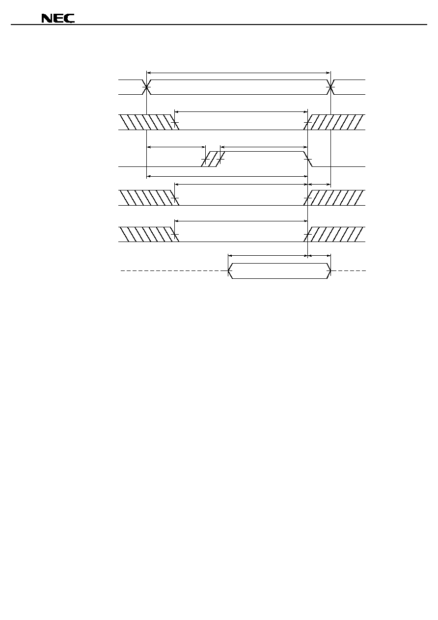
Figure 10. Sector / Chip Erase Timing Chart (Flash Memory)
Address (Input)
/CEf (Input)
/OE (Input)
/WE (Input)
I/O (Input)
V
CC
f
t
DS
t
DH
t
CH
t
CS
t
WPH
555H
t
WC
t
AS
t
AH
t
WP
55H
AAH
80H
AAH
55H
(10H for chip erase)
30H
2AAH
555H
555H
2AAH
FSA
Note
t
GHWL
t
VCS
Note FSA is the sector address to be erased. In the case of chip erase, input 555H (WORD mode), AAAH (BYTE
mode).
Remark This timing chart shows the WORD mode's case. In the BYTE mode, address to be input are different from
the WORD mode. See Command Sequence (Flash Memory)..
Figure 11. Data Polling Timing Chart (Flash Memory)
/CEf (Input)
t
OEH
t
OE
t
BPG,
t
WPG,
t
SER
t
CEf
Hi-Z
t
CH
/OE (Input)
/WE (Input)
I/O7 (Output)
RY (/BY) (Output)
t
EOE
/I/O7
Valid data
Hi-Z
I/O0 - I/O6 (Output)
t
DF
t
BUSY
D
OUT
Note
Status data
Note I/O7 = D
OUT
: True value of program data (indicates completion of automatic program / erase)

Data Sheet M15318EJ2V0DS
25
MC-222244A-X
Figure 12. Toggle Bit Timing Chart (Flash Memory)
/OE (Input)
/WE (Input)
/CEf (Input)
Address (Input)
I/O6, I/O2 (Input / Output)
t
AS
t
ASO
t
AHT
t
AHT
t
CEPH
t
OEPH
t
OEH
t
BUSY
t
DH
t
OEH
t
CEf
t
OE
Input data
Toggle
Toggle
Valid
data out
Stop
toggling
Note
Toggle
RY (/BY) (Output)
Note I/O6 stops the toggle (indicates automatic program / erase completion).
Figure 13. I/O2 vs. I/O6 Timing Chart (Flash Memory)
/WE (Input)
Input of automatic
erase command
Erase
suspended
Erasure resumed
Erase suspended input
of program command
Erase suspended input
of program command
Erase suspended
read
Erase suspended
read
Erasure
Erasure Completion of
erasure
Toggle
I/O6 (Output)
I/O2 (Output)
I/O2 and I/O6 (/CEf or /OE is used for toggle)
Figure 14. RY (/BY) (Ready / Busy) Timing Chart (Flash Memory)
/CEf (Input)
/WE (Input)
RY (/BY) (Output)
t
BUSY
Automatic program or erase
Rising edge of the last write pulse
Figure 15. /RESET and RY (/BY) Timing Chart (Flash Memory)
/WE (Input)
/RESET (Input)
RY (/BY) (Output)
t
RP
t
READY
t
RB

Data Sheet M15318EJ2V0DS
26
MC-222244A-X
Figure 16. Write CIOf Timing Chart (Flash Memory)
/CEf, /WE (Input)
CIOf (Input)
Input determined
t
AH
t
AS
Falling edge of last write pulse
Figure 17. BYTE mode Switching Timing Chart (Flash Memory)
/CEf (Input)
CIOf (Input)
I/O0 - I/O14 (Output)
Hi-Z
I/O15 (Output), A
-
1 (Input)
t
ELFL
t
ACC
t
FLQZ
Hi-Z
Hi-Z
Data Output
I/O0-I/O14
Data Output
I/O15
Data Output
I/O0-I/O7
Address Input
A
-
1
Figure 18. WORD mode Switching Timing Chart (Flash Memory)
Data Output
I/O15
/CEf (Input)
CIOf (Input)
I/O0 - I/O14 (Output)
I/O15 (Output), A
-
1 (Input)
t
ELFH
t
FHQV
t
CEf
Hi-Z
Hi-Z
Hi-Z
Data Output
I/O0-I/O14
Data Output
I/O0-I/O7
Address Input
A
-
1

Data Sheet M15318EJ2V0DS
27
MC-222244A-X
Figure 19. Read Cycle Timing Chart (SRAM)
t
HZ2
t
RC
t
OH
t
HZ1
t
BLZ
t
BA
t
LZ2
t
CO2
t
LZ1
t
CO1
t
BHZ
t
AA
Hi-Z
Data out
/LB, /UB (Input)
CE2s (Input)
/CE1s (Input)
Address (Input)
I/O (Output)
t
OLZ
t
OE
t
OHZ
/OE (Input)
Remark In read cycle, /WE should be fixed to high level.

Data Sheet M15318EJ2V0DS
28
MC-222244A-X
Figure 20. Write Cycle Timing Chart 1 (/WE Controlled) (SRAM)
t
WC
t
CW1
t
BW
t
WHZ
t
DW
t
DH
t
OW
Indefinite data out
Hi-Z
Hi-Z
Data in
Indefinite data out
Address (Input)
/CE1s (Input)
/LB, /UB (Input)
I/O (Input / Output)
CE2s (Input)
t
CW2
t
AW
t
WP
t
AS
t
WR
/WE (Input)
Cautions 1. During address transition, at least one of pins /CE1s, CE2s, /WE should be inactivated.
2. Do not input data to the I/O pins while they are in the output state.
Remarks 1. Write operation is done during the overlap time of a low level /CE1s, /WE, /LB and/or /UB, and a
high level CE2s.
2. If /CE1s changes to low level at the same time or after the change of /WE to low level, or if
CE2s changes to high level at the same time or after the change of /WE to low level, the I/O
pins will remain Hi-Z state.
3. When /WE is at low level, the I/O pins are always Hi-Z. When /WE is at high level, read
operation is executed. Therefore /OE should be at high level to make the I/O pins Hi-Z.

Data Sheet M15318EJ2V0DS
29
MC-222244A-X
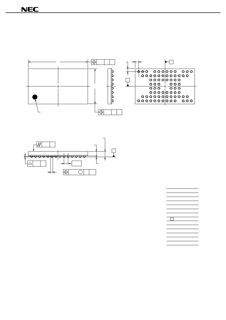
Figure 21. Write Cycle Timing Chart 2 (/CE1s Controlled) (SRAM)
t
WC
t
AS
t
CW1
t
DW
t
DH
Data in
Hi-Z
Address (Input)
/CE1s (Input)
/LB, /UB (Input)
I/O (Input)
Hi-Z
CE2s (Input)
t
CW2
t
AW
t
WP
t
WR
/WE (Input)
t
BW
Cautions 1. During address transition, at least one of pins /CE1s, CE2s, /WE should be inactivated.
2. Do not input data to the I/O pins while they are in the output state.
Remark Write operation is done during the overlap time of a low level /CE1s, /WE, /LB and/or /UB, and a high level
CE2s.
Data Sheet M15318EJ2V0DS
30
MC-222244A-X
Figure 22. Write Cycle Timing Chart 3 (CE2s Controlled) (SRAM)
t
WC
t
AS
t
CW2
t
BW
t
DW
t
DH
Data in
Hi-Z
Address (Input)
CE2s (Input)
/LB, /UB (Input)
I/O (Input)
Hi-Z
/CE1s (Input)
t
CW1
t
AW
t
WP
t
WR
/WE (Input)
Cautions 1. During address transition, at least one of pins /CE1s, CE2s, /WE should be inactivated.
2. Do not input data to the I/O pins while they are in the output state.
Remark Write operation is done during the overlap time of a low level /CE1s, /WE, /LB and/or /UB, and a high level
CE2s.

Data Sheet M15318EJ2V0DS
31
MC-222244A-X
Figure 23. Write Cycle Timing Chart 4 (/LB, /UB Controlled) (SRAM)
t
WC
t
DW
t
DH
Data in
Hi-Z
Address (Input)
/LB, /UB (Input)
I/O (Input)
Hi-Z
CE2s (Input)
t
CW2
t
AW
t
WP
t
WR
/WE (Input)
t
AS
t
BW
/CE1s (Input)
t
CW1
Cautions 1. During address transition, at least one of pins /CE1s, CE2s, /WE should be inactivated.
2. Do not input data to the I/O pins while they are in the output state.
Remark Write operation is done during the overlap time of a low level /CE1s, /WE, /LB and/or /UB, and a high level
CE2s.

Data Sheet M15318EJ2V0DS
32
MC-222244A-X
Figure 24. Data Retention Timing Chart 1 (/CE1s Controlled) (SRAM)
V
IH
(MIN.)
V
CCDR
(MIN.)
V
IL
(MAX.)
/CE1s
/CE1s
V
CC
s ≠ 0.2 V
V
SS
V
CC
s
V
CC
s(MIN.)
t
CDR
Data retention mode
t
R
Remark
On the data retention mode by controlling /CE1s, the input level of CE2s must be
V
CC
s
-
0.2 V or
0.2 V. The other pins (Address, I/O, /WE, /OE, /LB, /UB) can be in Hi-Z state.
Figure 25. Data Retention Timing Chart 2 (CE2s Controlled) (SRAM)
V
IH
(MIN.)
V
CCDR
(MIN.)
V
IL
(MAX.)
CE2s
CE2s
0.2 V
V
SS
t
CDR
Data retention mode
t
R
V
CC
s
V
CC
s(MIN.)
Remark
On the data retention mode controlling CE2s, the other pins (/CE1s, Address, I/O, /WE, /OE, /LB, /UB)
can be in Hi-Z state.

Data Sheet M15318EJ2V0DS
33
MC-222244A-X
Figure 26. Data Retention Timing Chart 3 (/LB, /UB Controlled) (SRAM)
t
CDR
Data retention mode
V
IH
(MIN.)
V
CCDR
(MIN.)
V
IL
(MAX.)
t
R
/LB, /UB
/LB, /UB
V
CC
s ≠ 0.2 V
V
SS
V
CC
s
V
CC
s(MIN.)
Remark
On the data retention mode by controlling /LB and /UB, the input level of /CE1s and CE2s must be
V
CC
s
-
0.2 V or
0.2 V. The other pins (Address, I/O, /WE, /OE) can be in Hi-Z state.
Flow Charts (Flash Memory)
Refer to DUAL OPERATION FLASH MEMORY 32M BITS A SERIES Information (M14914E).

Data Sheet M15318EJ2V0DS
34
MC-222244A-X
CFI Code List
(1/2)
Address A6 to A0
Data I/O15 to I/O0
Description
10H
0051H
"QRY" (ASCII code)
11H
0052H
12H
0059H
13H
0002H
Main command set
14H
0000H
2 : AMD/FJ standard type
15H
0040H
Start address of PRIMARY table
16H
0000H
17H
0000H
Auxiliary command set
18H
0000H
00H : Not supported
19H
0000H
Start address of auxiliary algorithm table
1AH
0000H
1BH
0027H
Minimum V
CC
f voltage (program / erase)
I/O7 to I/O4 : 1 V/bit
I/O3 to I/O0 : 100 mV/bit
1CH
0036H
Maximum V
CC
f voltage (program / erase)
I/O7 to I/O4 : 1 V/bit
I/O3 to I/O0 : 100 mV/bit
1DH
0000H
Minimum V
PP
voltage
1EH
0000H
Maximum V
PP
voltage
1FH
0004H
Typical word program time (2
N
µ
s)
20H
0000H
Typical buffer program time (2
N
µ
s)
21H
000AH
Typical sector erase time (2
N
ms)
22H
0000H
Typical chip erase time (2
N
ms)
23H
0005H
Maximum word program time (typical time
◊
2
N
)
24H
0000H
Maximum buffer program time (typical time
◊
2
N
)
25H
0004H
Maximum sector erasing time (typical time
◊
2
N
)
26H
0000H
Maximum chip erasing time (typical time
◊
2
N
)
27H
0016H
Capacity (2
N
Bytes)
28H
0002H
I/O information
29H
0000H
2 :
◊
8/
◊
16-bit organization
2AH
0000H
Maximum number of bytes when two banks are programmed (2
N
)
2BH
0000H
2CH
0002H
Type of erase block
2DH
0007H
Information about erase block 1
2EH
0000H
Bit0 to 15 : y = number of sectors
2FH
0020H
Bit16 to 31 : z = size
30H
0000H
(Z
◊
256 Bytes)

Data Sheet M15318EJ2V0DS
35
MC-222244A-X
(2/2)
Address A6 to A0
Data I/O15 to I/O0
Description
31H
003EH
Information about erase block 2
32H
0000H
bit0 to 15 : y = number of sectors
33H
0000H
bit16 to 31 : z = size
34H
0001H
(z
◊
256 Bytes)
40H
0050H
"PRI" (ASCII code)
41H
0052H
42H
0049H
43H
0031H
Main version (ASCII code)
44H
0032H
Minor version (ASCII code)
45H
0000H
Address during command input
00H : Necessary
01H : Unnecessary
46H
0002H
Temporary erase suspend function
00H : Not supported
01H : Read only
02H : Read / Program
47H
0001H
Sector group protection
00H : Not supported
01H : Supported
48H
0001H
Temporary sector group protection
00H : Not supported
01H : Supported
49H
0004H
Sector group protection algorithm
4AH
00xxH
Number of sectors of bank 2
00H : Not supported
20H : MC-222244A-X
4BH
0000H
Burst mode
00H : Not supported
4CH
0000H
Page mode
00H : Not supported
4DH
0085H
Minimum V
ACC
voltage
I/O7 to I/O4 : 1 V/bit
I/O3 to I/O0 : 100 mV/bit
4EH
0095H
Maximum V
ACC
voltage
I/O7 to I/O4 : 1 V/bit
I/O3 to I/O0 : 100 mV/bit
4FH
00xxH
Boot organization
03H : Top boot
50H
0001H
Temporary program suspend function
00H : Not supported
01H : Supported
Data Sheet M15318EJ2V0DS
36
MC-222244A-X
Package Drawing
77-PIN TAPE FBGA (12x7)
S
x
e
AB
M
S
w
B
w
S A
S
y
S
y1
ITEM
MILLIMETERS
D
12.0
±
0.1
7.0
±
0.1
E
0.2
b
0.45
±
0.05
x
0.08
y
0.1
y1
0.1
ZD
0.7
ZE
0.8
w
A
1.1
±
0.1
A1
0.26
±
0.05
A2
0.84
P77F9-80-BT3
b
INDEX MARK
A
0.8
e
A1
A2
S
A
B
ZD
ZE
P N M L K J H G F E D C B A
8
7
6
5
4
3
2
1
D
E

Data Sheet M15318EJ2V0DS
37
MC-222244A-X
Recommended Soldering Conditions
Please consult with our sales offices for soldering conditions of the MC-222244A-X.
Type of Surface Mount Device
MC-222244AF9-B85X-BT3 : 77-pin TAPE FBGA (12
◊
7)

Data Sheet M15318EJ2V0DS
38
MC-222244A-X
[ MEMO ]

Data Sheet M15318EJ2V0DS
39
MC-222244A-X
NOTES FOR CMOS DEVICES
1
PRECAUTION AGAINST ESD FOR SEMICONDUCTORS
Note:
Strong electric field, when exposed to a MOS device, can cause destruction of the gate oxide and
ultimately degrade the device operation. Steps must be taken to stop generation of static electricity
as much as possible, and quickly dissipate it once, when it has occurred. Environmental control
must be adequate. When it is dry, humidifier should be used. It is recommended to avoid using
insulators that easily build static electricity. Semiconductor devices must be stored and transported
in an anti-static container, static shielding bag or conductive material. All test and measurement
tools including work bench and floor should be grounded. The operator should be grounded using
wrist strap. Semiconductor devices must not be touched with bare hands. Similar precautions need
to be taken for PW boards with semiconductor devices on it.
2
HANDLING OF UNUSED INPUT PINS FOR CMOS
Note:
No connection for CMOS device inputs can be cause of malfunction. If no connection is provided
to the input pins, it is possible that an internal input level may be generated due to noise, etc., hence
causing malfunction. CMOS devices behave differently than Bipolar or NMOS devices. Input levels
of CMOS devices must be fixed high or low by using a pull-up or pull-down circuitry. Each unused
pin should be connected to V
DD
or GND with a resistor, if it is considered to have a possibility of
being an output pin. All handling related to the unused pins must be judged device by device and
related specifications governing the devices.
3
STATUS BEFORE INITIALIZATION OF MOS DEVICES
Note:
Power-on does not necessarily define initial status of MOS device. Production process of MOS
does not define the initial operation status of the device. Immediately after the power source is
turned ON, the devices with reset function have not yet been initialized. Hence, power-on does
not guarantee out-pin levels, I/O settings or contents of registers. Device is not initialized until the
reset signal is received. Reset operation must be executed immediately after power-on for devices
having reset function.

MC-222244A-X
Related Documents
Document Name
Document Number
DUAL OPERATION FLASH MEMORY 32M BITS A SERIES Information
M14914E
M8E 00. 4
The information in this document is current as of July, 2001. The information is subject to change
without notice. For actual design-in, refer to the latest publications of NEC's data sheets or data
books, etc., for the most up-to-date specifications of NEC semiconductor products. Not all products
and/or types are available in every country. Please check with an NEC sales representative for
availability and additional information.
No part of this document may be copied or reproduced in any form or by any means without prior
written consent of NEC. NEC assumes no responsibility for any errors that may appear in this document.
NEC does not assume any liability for infringement of patents, copyrights or other intellectual property rights of
third parties by or arising from the use of NEC semiconductor products listed in this document or any other
liability arising from the use of such products. No license, express, implied or otherwise, is granted under any
patents, copyrights or other intellectual property rights of NEC or others.
Descriptions of circuits, software and other related information in this document are provided for illustrative
purposes in semiconductor product operation and application examples. The incorporation of these
circuits, software and information in the design of customer's equipment shall be done under the full
responsibility of customer. NEC assumes no responsibility for any losses incurred by customers or third
parties arising from the use of these circuits, software and information.
While NEC endeavours to enhance the quality, reliability and safety of NEC semiconductor products, customers
agree and acknowledge that the possibility of defects thereof cannot be eliminated entirely. To minimize
risks of damage to property or injury (including death) to persons arising from defects in NEC
semiconductor products, customers must incorporate sufficient safety measures in their design, such as
redundancy, fire-containment, and anti-failure features.
NEC semiconductor products are classified into the following three quality grades:
"Standard", "Special" and "Specific". The "Specific" quality grade applies only to semiconductor products
developed based on a customer-designated "quality assurance program" for a specific application. The
recommended applications of a semiconductor product depend on its quality grade, as indicated below.
Customers must check the quality grade of each semiconductor product before using it in a particular
application.
"Standard": Computers, office equipment, communications equipment, test and measurement equipment, audio
and visual equipment, home electronic appliances, machine tools, personal electronic equipment
and industrial robots
"Special":
Transportation equipment (automobiles, trains, ships, etc.), traffic control systems, anti-disaster
systems, anti-crime systems, safety equipment and medical equipment (not specifically designed
for life support)
"Specific": Aircraft, aerospace equipment, submersible repeaters, nuclear reactor control systems, life
support systems and medical equipment for life support, etc.
The quality grade of NEC semiconductor products is "Standard" unless otherwise expressly specified in NEC's
data sheets or data books, etc. If customers wish to use NEC semiconductor products in applications not
intended by NEC, they must contact an NEC sales representative in advance to determine NEC's willingness
to support a given application.
(Note)
(1) "NEC" as used in this statement means NEC Corporation and also includes its majority-owned subsidiaries.
(2) "NEC semiconductor products" means any semiconductor product developed or manufactured by or for
NEC (as defined above).
∑
∑
∑
∑
∑
∑