
The information in this document is subject to change without notice. Before using this document, please
confirm that this is the latest version.
Not all devices/types available in every country. Please check with local NEC representative for
availability and additional information.
©
2001
Document No. M15406EJ8V0DS00 (8th edition)
Date Published October 2002 NS CP (K)
Printed in Japan
MOS INTEGRATED CIRCUIT
µ
µ
µ
µ
PD4632312-X
32M-BIT CMOS MOBILE SPECIFIED RAM
2M-WORD BY 16-BIT
EXTENDED TEMPERATURE OPERATION
DATA SHEET
The mark
5
5
5
5
shows major revised points.
Description
The
µ
PD4632312-X is a high speed, low power, 33,554,432 bits (2,097,152 words by 16 bits) CMOS mobile
specified RAM featuring low power static RAM compatible function and pin configuration.
The
µ
PD4632312-X is fabricated with advanced CMOS technology using one-transistor memory cell.
The
µ
PD4632312-X is packed in 77-pin TAPE FBGA.
Features
∑
2,097,152 words by 16 bits organization
∑
Fast access time: 85, 95 ns (MAX.)
∑
Fast page access time: 35, 40 ns (MAX.)
∑
Byte data control: /LB (I/O0 to I/O7), /UB (I/O8 to I/O15)
∑
Low voltage operation: V
CC
= 2.6 to 3.1 V (-B85X)
V
CC
= 2.6 to 3.1 V (Chip), V
CC
Q = 1.65 to 1.95 V (I/O) (-BE95X)
∑
Operating ambient temperature: T
A
= ≠25 to +85 ∞C
∑
Output Enable input for easy application
∑
Chip Enable input: /CS pin
∑
Standby Mode input: MODE pin
∑
Standby Mode1: Normal standby (Memory cell data hold valid)
∑
Standby Mode2: Density of memory cell data hold is variable
µ
PD4632312
Access
Operating
Operating
Supply current
time
supply voltage
ambient
At operating
At standby
µ
A (MAX.)
ns (MAX.)
V
temperature mA (MAX.)
Density of data hold
Chip
I/O
∞C
32M bits 16M bits 8M bits 4M bits 0M bit
-B85X
85
2.6 to 3.1
≠
≠25 to +85
35
100
70
60
50
10
-BE95X
Note
95
2.6 to 3.1 1.65 to 1.95
Note Under development
Data Sheet M15406EJ8V0DS
3
µ
µ
µ
µ
PD4632312-X
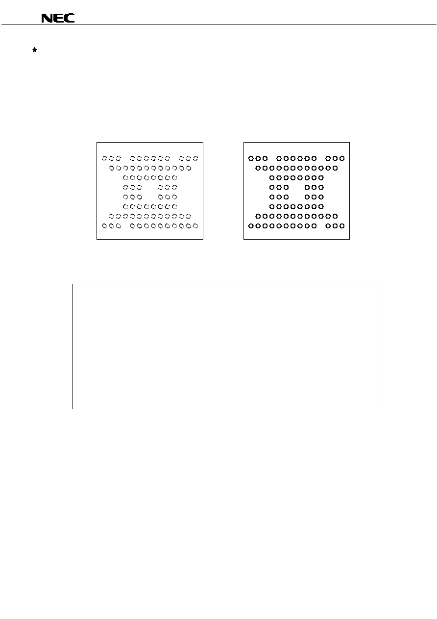
Pin Configurations
/xxx indicates active low signal.
77-pin TAPE FBGA (12 x 7)
[
µ
µ
µ
µ
PD4632312F9-B85X-BT3]
Top View
GND
I/O9
I/O5
A7
/OE
I/O7
I/O4
I/O0
A6
A18
A11
A8
A5
I/O8
I/O12
A13
A17
NC
NC
I/O10
NC
/WE
V
CC
A16
I/O11
NC
NC
A12
I/O6
I/O13
A9
A15
A19
I/O14
/CS
I/O15
I/O1
A1
A2
A4
A10
NC
I/O2
A0
A3
MODE
A20
A14
/LB
NC
NC
/UB
I/O3
NC
NC
GND
Top View
Bottom View
8
7
6
5
4
3
2
1
8
7
6
5
4
3
2
1
P N M L K J H G F E D C B A
A B C D E F G H J K L M N P
A
B
C
D
E
F
G
H
J
K
L
M
N
P
NC
NC
NC
NC
NC
NC
NC
NC
NC
NC
NC
NC
NC
NC
NC
NC
NC
NC
NC
NC
NC
Note Some signals can be applied because this pin is not internally connected.
Remark Refer to Package Drawing for the index mark.
A0 to A20
: Address inputs
I/O0 to I/O15 : Data inputs / outputs
/CS
: Chip Select
MODE
: Standby mode
/WE
: Write enable
/OE
: Output enable
/LB, /UB
: Byte data select
V
CC
: Power supply
GND
: Ground
NC
Note
: No Connection

Data Sheet M15406EJ8V0DS
4
µ
µ
µ
µ
PD4632312-X
77-pin TAPE FBGA (12 x 7)
[
µ
µ
µ
µ
PD4632312F9-BE95X-BT3]
Top View
GND
I/O9
I/O5
A7
/OE
I/O7
I/O4
I/O0
A6
A18
A11
A8
A5
I/O8
I/O12
A13
A17
NC
NC
I/O10
NC
/WE
V
CC
A16
I/O11
NC
NC
A12
I/O6
I/O13
A9
A15
A19
I/O14
/CS
I/O15
I/O1
A1
A2
A4
A10
V
CC
Q
I/O2
A0
A3
MODE
A20
A14
/LB
NC
NC
/UB
I/O3
NC
NC
GND
Top View
Bottom View
8
7
6
5
4
3
2
1
8
7
6
5
4
3
2
1
P N M L K J H G F E D C B A
A B C D E F G H J K L M N P
A
B
C
D
E
F
G
H
J
K
L
M
N
P
NC
NC
NC
NC
NC
NC
NC
NC
NC
NC
NC
NC
NC
NC
NC
NC
NC
NC
NC
NC
NC
Note Some signals can be applied because this pin is not internally connected.
Remark Refer to Package Drawing for the index mark.
A0 to A20
: Address inputs
I/O0 to I/O15 : Data inputs / outputs
/CS
: Chip Select
MODE
: Standby mode
/WE
: Write enable
/OE
: Output enable
/LB, /UB
: Byte data select
V
CC
: Power supply
V
CC
Q
: Input / Output power supply
GND
: Ground
NC
Note
: No Connection

