
The information in this document is subject to change without notice. Before using this document, please
confirm that this is the latest version.
Not all devices/types available in every country. Please check with local NEC representative for
availability and additional information.
©
2001
MOS INTEGRATED CIRCUIT
MC-2311100
MCP (MULTI-CHIP PACKAGE) MOBILE SPECIFIED RAM AND SRAM
16M-BIT CMOS MOBILE SPECIFIED RAM AND 4M-BIT CMOS SRAM
PRELIMINARY DATA SHEET
Document No. M15432EJ1V0DS00 (1st edition)
Date Published November 2001 NS CP (K)
Printed in Japan
The mark
5
5
5
5
shows major revised points.
Description
The MC-2311100 is a stacked type MCP (Multi-Chip Package) of 16,777,216 bits (1,048,576 words by 16 bits) Mobile
specified RAM and 4,194,304 bits (BYTE mode : 524,288 words by 8 bits, WORD mode : 262,144 words by 16 bits)
SRAM.
The MC-2311100 is packaged in a 61-pin TAPE FBGA.
General Features
∑
Supply voltage : V
CC
m / V
CC
s = 2.6 to 3.0 V
∑
Wide operating temperature : T
A
=
-
20 to +70
∞
C
∑
Output Enable input for easy application
∑
Byte data control : /LB (I/O0 to I/O7), /UB (I/O8 to I/O15)
Mobile specified RAM Features
∑
Memory organization : 1,048,576 words by 16 bits
∑
Fast access time : t
AA
= 80, 90, 100 ns (MAX.)
∑
Supply current : At operating : 35 mA (MAX.)
At Standby Mode 1 : 100
µ
A (MAX.) Normal standby (Memory cell data hold valid)
At Standby Mode 2 : 10
µ
A (MAX.) Memory cell data hold invalid
∑
Chip Enable inputs : /CEm
∑
Standby Mode input : MODE
SRAM Features
∑
Memory organization : 524,288 words
◊
8 bits (BYTE mode)
262,144 words
◊
16 bits (WORD mode)
∑
Fast access time : t
AA
= 70 ns (MAX.)
∑
Supply current : At operating : 40 mA (MAX.)
At Standby Mode : 7
µ
A (MAX.)
∑
Low V
CC
data retention: 1.0 V (MIN.)
∑
Two Chip Enable inputs: /CE1s, CE2s
Preliminary Data Sheet M15432EJ1V0DS
3
MC-2311100
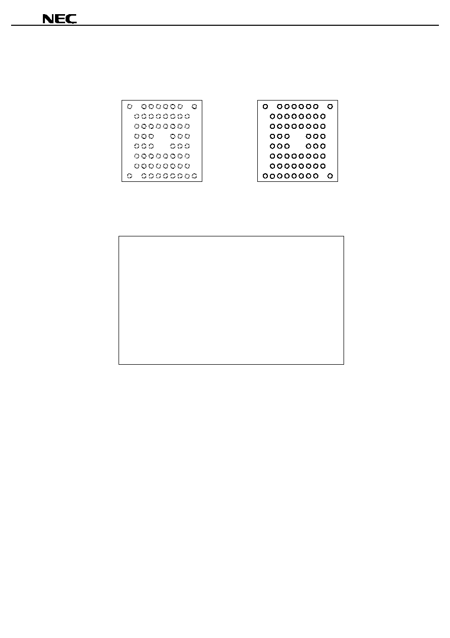
Pin Configuration
/xxx indicates active low signal.
61-pin TAPE FBGA (9
◊
◊
◊
◊
7)
Top View
Top View
Bottom View
8
7
6
5
4
3
2
1
8
7
6
5
4
3
2
1
A
B
C
D
E
F
G
H
J
K
NC
NC
NC
NC
NC
V
SS
A17
SA
A16
I/O6
I/O1
A1
A4
A10
A0
A14
V
SS
A7
A11
A8
/WE
/LB
NC
I/O8
I/O14
I/O5
CIOs
I/O2
I/O11
A6
CE2
A12
A15
A19
A3
MODE
/UB
I/O0
V
CC
s
I/O7
V
SS
I/O12
/CEm
V
CC
m
I/O10
A18
A5
A13
NC
A9
A2
NC
NC
I/O9
/OE
I/O15
I/O3
I/O13
/CE1s
I/O4
NC
A B C D E F G H J K
K J H G F E D C B A
Common Pins
A0 - A19
: Address inputs
I/O0 - I/O15 : Data inputs / outputs
/OE
: Output Enable
/WE
: Write Enable
/LB, /UB
: Byte data select
V
SS
: Ground
NC
Note
: No Connection
Mobile specified RAM Pins
/CEm
: Chip Enable
MODE
: Standby mode select
V
CC
m
: Supply Voltage
SRAM Pins
/CE1s
: Chip Enable
CE2s
: Chip Enable
SA
: Address input (A18)
CIOs
: Selects 8-bit or 16-bit mode
V
CC
s
: Supply Voltage
Note Some signals can be applied because this pin is not internally connected.
Remark Refer to 5. Package Drawing for the index mark.

Preliminary Data Sheet M15432EJ1V0DS
5
MC-2311100
CONTENTS
1. Bus Operations ...................................................................................................................................................6
2. Mobile specified RAM .........................................................................................................................................7
2.1
Initialization.................................................................................................................................................7
2.2
Standby Mode .............................................................................................................................................8
2.2.1
Standby Mode State Machine ................................................................................................................8
3. Electrical Specifications.....................................................................................................................................9
4. Timing Charts ....................................................................................................................................................19
5. Package Drawing ..............................................................................................................................................42
6. Recommended Soldering Conditions .............................................................................................................43

