Document Outline
- COVER
- Features
- Ordering Information
- Pin Configuration
- Block Diagram
- Electrical Specifications
- Package Drawing

The information in this document is subject to change without notice. Before using this document, please
confirm that this is the latest version.
Not all products and/or types are available in every country. Please check with NEC Electronics sales
representative for availability and additional information.
MOS INTEGRATED CIRCUIT
MC-22222361-X
MCP (MULTI-CHIP PACKAGE) FLASH MEMORY AND SRAM
64M-BIT PAGE MODE FLASH MEMORY AND 8M-BIT SRAM
PRELIMINARY DATA SHEET
Document No. M15854EJ4V0DS00 (4th edition)
Date Published November 2002 NS CP (K)
Printed in Japan
The mark
#
#
#
# shows major revised points.
2002
Description
The MC-22222361-X is a stacked type MCP (Multi-Chip Package) of 67,108,864 bits (4,194,304 words by 16 bits)
flash memory and 8,388,608 bits (524,288 words by 16 bits) static RAM.
The MC-22222361-X is packaged in a 85-pin TAPE FBGA .
Features
General Features
∑ Fast access time : t
ACC
= 80 ns (MAX.) (V
CC
f = 1.8 V), 85 ns (MAX.) (V
CC
f = 1.65 V) (Flash Memory),
t
AA
= 55 ns (MAX.) (SRAM)
∑ Supply voltage : -D80X : 1.8 to 2.1 V (Chip) / 2.7 to 3.1 V (I/O) (Flash Memory), 2.7 to 3.1 V (SRAM)
-E85X : 1.65 to 1.95 V (Chip) / 2.7 to 3.1 V (I/O) (Flash Memory), 2.7 to 3.1 V (SRAM)
∑ Output Enable input for easy application
∑ Wide operating temperature : T
A
=
-25 to +85∞C
Flash Memory Features
∑ Four bank organization enabling simultaneous execution of program / erase and read
∑ High-speed read with page mode
∑ Bank organization : 4 banks (8M bits + 24M bits + 24M bits + 8M bits)
∑ Memory organization : 4,194,304 words ◊ 16 bits
∑ Sector organization : 142 sectors (4K words ◊ 16 sectors, 32K words ◊ 126 sectors)
Boot sector allocated to the highest address (sector) and the lowest address (sector)
∑ 3-state output
∑ Automatic program
∑ Program suspend / resume
∑ Unlock bypass program
∑ Automatic erase
∑ Chip erase
∑ Sector erase (sectors can be combined freely)
∑ Erase suspend / resume
∑ Program / Erase completion detection
∑ Detection through data polling and toggle bits
∑ Detection through RY (/BY) pin
∑ Sector group protection
∑ Any sector group can be protected
∑ Any protected sector group can be temporary unprotected
∑ Any sector group can be unprotected
∑ Sectors can be used for boot application
Preliminary Data Sheet M15854EJ4V0DS
2
MC-22222361-X
∑ Hardware reset and standby using /RESET pin
∑ Automatic sleep mode
∑ Boot block sector protect by /WP (ACC) pin
∑ Extra One Time Protect Sector provided
∑ Program / erase time
∑ Program : 11.0
µs / word (TYP.)
∑ Sector erase :
Program / erase cycle : 100,000 cycles
0.15 s (TYP.) (4K words sector), 0.5 s (TYP.) (32K words sector)
Program / erase cycle : 300,000 cycles
0.5 s (TYP.) (4K words sector), 0.7 s (TYP.) (32K words sector)
∑ Program / erase cycle : 300,000 cycles (MIN.)
SRAM Features
∑ Memory organization : 524,288 words ◊ 16 bits
∑ Supply current : At operating : 30 mA (MAX.)
At standby : 15
µA (MAX.)
∑ Two Chip Enable inputs : /CE1s, CE2s
∑ Byte data control : /LB, /UB
∑ Low V
CC
data retention : 1.5 V (MIN.)
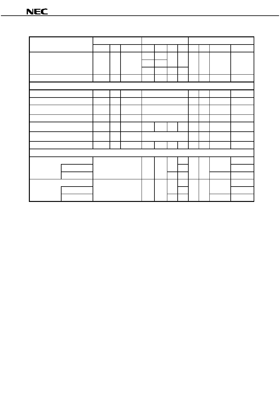
Ordering Information
Part number
Flash Memory
SRAM
Operating supply voltage
Package
Mounted
Access time
Access time
V
Flash Memory
ns (MAX.)
ns (MAX.)
Chip
I/O
MC-22222361F9-D80X-CD5
80
55
1.8 to 2.1
2.7 to 3.1
85-pin
µPD29F064115-X
(Flash
(Flash
TAPE FBGA
Memory)
Memory)
(11
◊ 8)
2.7 to 3.1
(SRAM)
MC-22222361F9-E85X-CD5
85
1.65 to 1.95
(Flash
Memory)
2.7 to 3.1
(SRAM)
Bus Operations, COMMANDS, HARDWARE SEQUENCE FLAGS, HARD WARE DATA PROTECTION, READ
MODE REGISTER SETTINGS, TIMING CHARTS and FLOW CHARTS for Flash Memory, refer to PAGE MODE
FLASH MEMORY, BURST MODE FLASH MEMORY Information (M15451E).
TIMING CHARTS OF SRAM FOR MCP, refer to SRAM AND MOBILE SPECIFIED RAM TIMING CHARTS FOR
MCP Information (M15819E).
Preliminary Data Sheet M15854EJ4V0DS
3
MC-22222361-X
Pin Configuration
/xxx indicates active low signal.
85-pin TAPE FBGA (11
◊
◊
◊
◊ 8)
Top View
Vss
I/O9
I/O5
A7
/OE
I/O7
I/O4
I/O0
A6
A18
A11
A8
A5
I/O8
I/O12
A13
A17
IC
/CEf
I/O10
V
CC
f
/WE
V
CC
s
A16
I/O11
RY(/BY)
/RESET
A12
I/O6
I/O13
A9
A15
A19
I/O14
/CE1s
I/O15
I/O1
A1
A2
A4
A10
V
CC
Qf
I/O2
A0
A3
CE2s
A20
A14
/LB
V
CC
s
/WP(ACC)
/UB
I/O3
A21
NC
Vss
A
B
C
D
E
F
G
H
NC
NC
NC
NC
NC
NC
NC
NC
NC
NC
NC
NC
NC
M
K
L
J
10
9
8
7
6
5
4
3
2
1
NC
NC
NC
NC
NC
NC
NC
NC
NC
NC
NC
NC
NC
NC
NC
NC
Top View
Bottom View
H
G
F
E
D
C
B
A
H G F E D C B A
M
K L
J
M
K
L
J
10
9
8
7
6
5
4
3
2
1
Common Pins
A0 to A18
: Address Inputs
I/O0 to I/O15 : Data Inputs / Outputs
/OE
: Output Enable Input
/WE
: Write Enable Input
V
SS
: Ground
NC
Note1
: No Connection
IC
Note2
: Internal Connection
Flash Memory Pins
A19 to A21 : Address Inputs
/CEf
: Chip Enable Input
RY (/BY)
: Ready (Busy) output
/RESET
: Hardware reset Input
/WP(ACC) : Hardware Write Protect (Acceleration) Input
V
CC
f
: Supply Voltage
V
CC
Qf
: Input / Output Supply Voltage
SRAM Pins
/CE1s
: Chip Enable 1 Input
CE2s
: Chip Enable 2 Input
/LB, /UB
: Byte data select Input
V
CC
s
: Supply Voltage
Notes 1. Some signals can be applied because this pin is not internally connected.
2. Any level (Vss, Vccf, Open) can be applied. Do not change the state during operation.
Remark Refer to Package Drawing for the index mark.
Preliminary Data Sheet M15854EJ4V0DS
4
MC-22222361-X
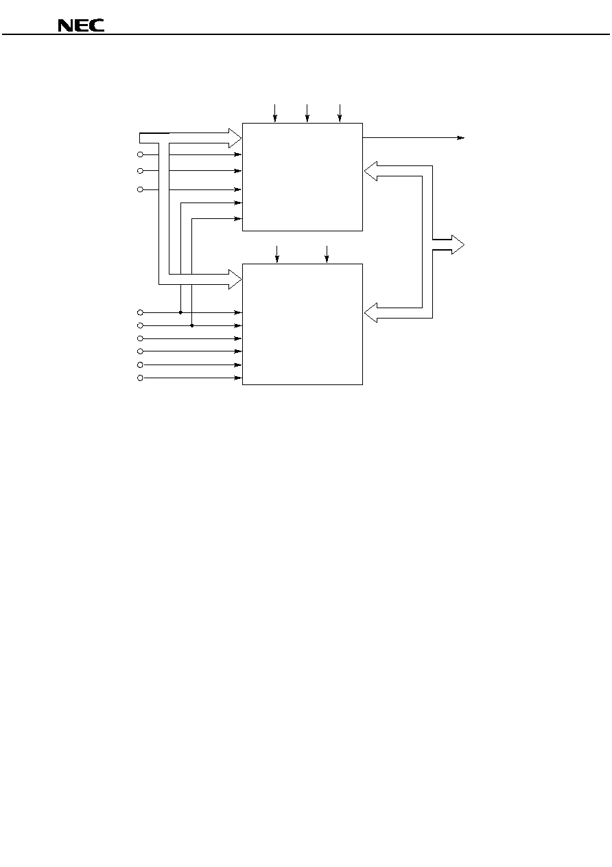
Block Diagram
64 M-bit Flash Memory
(4,194,304 words by 16 bits)
/WE
/OE
/CE1s
/RESET
/CEf
I/O0 to I/O15
A0 to A21
8 M-bit SRAM
(524,288 words by 16 bits)
RY (/BY)
A0 to A18
A0 to A21
V
CC
f
V
SS
V
CC
s
V
SS
CE2s
/LB
/UB
/WP(ACC)
V
CC
Qf
Preliminary Data Sheet M15854EJ4V0DS
5
MC-22222361-X
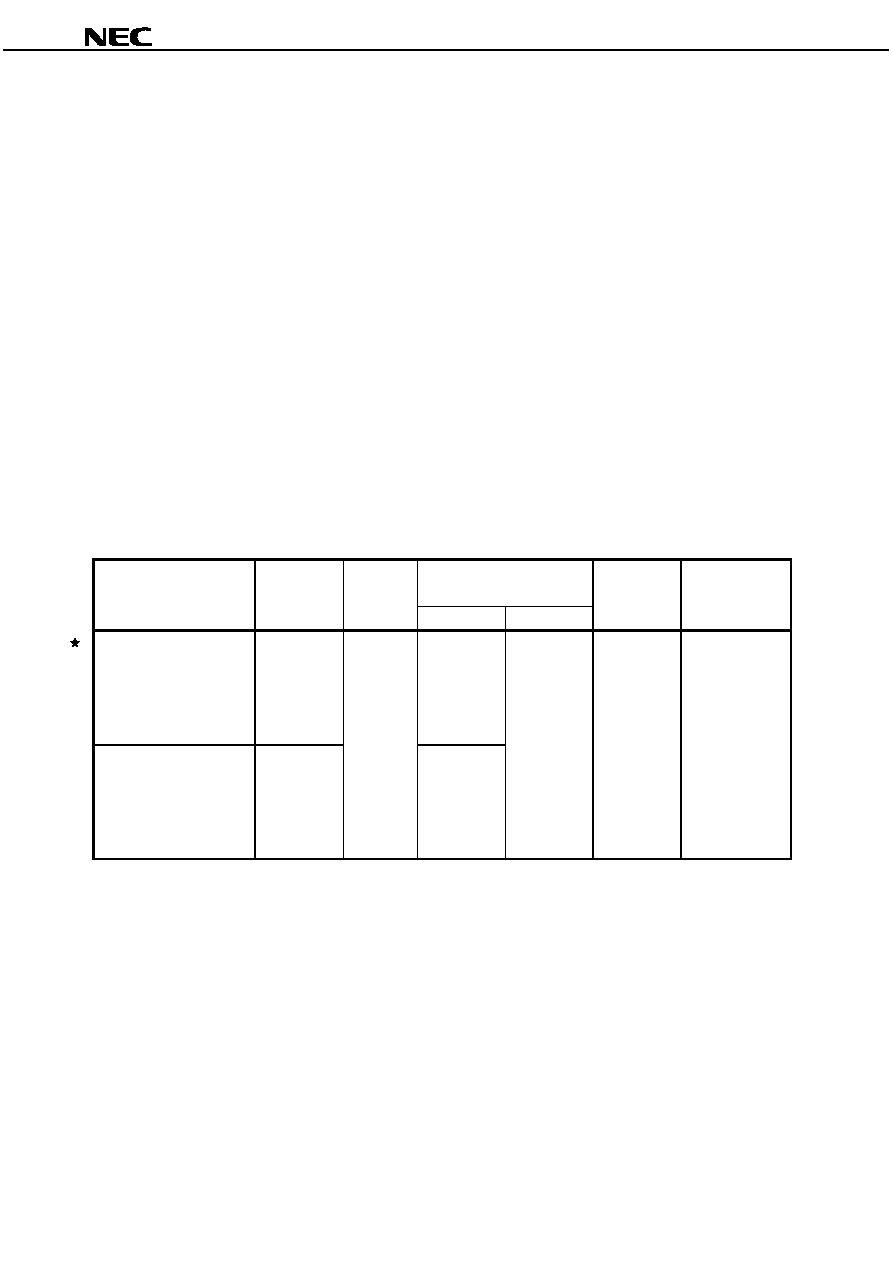
Bus Operations
Operation
Flash Memory
SRAM
Common
/RESET /CEf /WP(ACC) /CE1
S
CE2
S
/LB
/UB /OE /WE I/O0 to I/O7 I/O8 to I/O15
Full Standby
H
H
◊
H
◊
◊
◊
◊
◊
High-Z
High-Z
◊
L
◊
◊
H
H
Output Disable
H
L
◊
L
H
◊
◊
H
H
High-Z
High-Z
Flash Memory
Word Read
Note 1
H
L
◊
Note 2
L
H
Data Out
Data Out
Word Write
H
L
◊
Note 2
H
L
Data In
Data In
Temporary Sector Group Unprotect
V
ID
◊
◊
Note 2
◊
◊
High-Z or
Data In/Out
High-Z or
Data In/Out
Automatic Sleep Mode
H
L
◊
Note 2
L
H
Data Out
Data Out
Boot Block Sector Protect
◊
◊
L
◊
◊
◊
◊
◊
◊
High-Z or
Data In/Out
High-Z or
Data In/Out
Accelerated Mode
H
◊
V
ACC
Note 2
◊
◊
High-Z or
Data In/Out
High-Z or
Data In/Out
Hardware Reset
L
◊
◊
◊
◊
◊
◊
◊
◊
High-Z
High-Z
SRAM
Word Read
Note 3
L
H
L
L
L
H
Data Out
Data Out
Lower byte read
H
High-Z
Upper byte read
H
L
High-Z
Data Out
Word Write
Note 3
L
H
L
L
◊
L
Data In
Data In
Lower byte read
H
High-Z
Upper byte read
H
L
High-Z
Data In
Caution Other operations except for indicated in this table are inhibited.
Notes 1. When /OE = V
IL
, V
IL
can be applied to /WE. When /OE = V
IH
, a write operation is started. When /WE = V
IL
and /OE = V
IL
, a write operation is started.
2. SRAM should be Standby.
3. Flash Memory should be Standby or Hardware reset.
Remarks 1.
◊ : V
IH
or V
IL
, H : V
IH
, L : V
IL
, V
ID
: 9.0 to 11.0 V, V
ACC
: 8.5 to 9.5 V
2. Sector group protection and read the product ID are using a command.
3. If an address is held longer than the minimum read cycle time (t
RC
) in the flash memory read mode, the
automatic sleep mode is set.