Document Outline
- COVER
- Features
- Ordering Information
- Pin Configurations
- Block Diagram
- Electrical Specifications
- Package Drawings

The information in this document is subject to change without notice. Before using this document, please
confirm that this is the latest version.
Not all devices/types available in every country. Please check with local NEC representative for
availability and additional information.
©
2001
MOS INTEGRATED CIRCUIT
µ
PD23C256112A
NAND INTERFACE
256M-BIT MASK-PROGRAMMABLE ROM
DATA SHEET
Document No. M15902EJ2V0DS00 (2nd edition)
Date Published September 2002 NS CP (K)
Printed in Japan
The mark
5
5
5
5
shows major revised points
.
Description
The
µ
PD23C256112A is a 256 Mbit NAND interface programmable mask read-only memory that operates with a
single power supply. The memory organization consists of (512 + 16 (Redundancy)) bytes x 32 pages x 2,048 blocks.
The
µ
PD23C256112A is a serial type mask ROM in which addresses and commands are input and data output
serially via the I/O pins.
The
µ
PD23C256112A is packed in 48-pin PLASTIC TSOP(I).
Features
∑
Word organization
(33,554,432 + 1,048,576
Note
) words by 8 bits
∑
Page size
(512 + 16
Note
) by 8 bits
∑
Block size
(16,384 + 512
Note
) by 8 bits
Note Underlined parts are redundancy.
Caution Redundancy is not programmable parts and is fixed to all FFH.
∑
Operation mode
READ mode (1), READ mode (2), READ mode (3), RESET, STATUS READ, ID READ
∑
Operating supply voltage : V
CC
= 3.3
±
0.3 V
∑
Access Time
Memory cell array to starting address
: 7
µ
s (MAX.)
Read cycle time
: 50 ns (MIN.)
/RE access time
: 35 ns (MAX.)
∑
Operating supply current
During read
: 30 mA (MAX.) (50 ns cycle operation)
During standby (CMOS) : 100
µ
A (MAX.)
Ordering Information
Part Number
Package
µ
PD23C256112AGY-xxx-MJH
48-pin PLASTIC TSOP(I) (12x18) (Normal bent)
µ
PD23C256112AGY-xxx-MKH
48-pin PLASTIC TSOP(I) (12x18) (Reverse bent)
(xxx : ROM code suffix No.)

Data Sheet M15902EJ2V0DS
2
µ
PD23C256112A
Pin Configurations
/xxx indicates active low signal.
48-pin PLASTIC TSOP(I) (12x18) (Normal bent)
[
µ
µ
µ
µ
PD23C256112AGY-xxx-MJH ]
Marking Side
NC
NC
NC
IC
IC
GND
R, /B
/RE
/CE
NC
NC
V
CC
V
SS
NC
NC
CLE
ALE
/WE
IC
IC
IC
NC
NC
NC
NC
NC
NC
NC
I/O7
I/O6
I/O5
I/O4
NC
NC
NC
V
CC
V
SS
NC
NC
NC
I/O3
I/O2
I/O1
I/O0
NC
NC
NC
NC
1
2
3
4
5
6
7
8
9
10
11
12
13
14
15
16
17
18
19
20
21
22
23
24
48
47
46
45
44
43
42
41
40
39
38
37
36
35
34
33
32
31
30
29
28
27
26
25
I/O0 to I/O7
: Address Inputs / Command Inputs / Data Outputs
CLE
: Command Latch Enable Input
ALE
: Address Latch Enable Input
/WE
: Write Enable Input
/RE
: Read Enable Input
/CE
: Chip Enable Input
R, /B
Note1
: READY, /BUSY Output
V
CC
: Supply voltage
Vss
: Ground
NC
Note2
: No connection
IC
Note3
: Internal connection
GND
: GND
Notes 1. This pin is an open-drain output pin. Therefore, a pull-up resistor is required when using this pin.
2. Some signals can be applied because this pin is not connected to the inside of the chip.
3. Leave this pin unconnected or connected to V
SS
.
Remark Refer to Package Drawings for the 1-pin index mark.
Data Sheet M15902EJ2V0DS
3
µ
PD23C256112A
48-pin PLASTIC TSOP(I) (12x18) (Reverse bent)
[
µ
µ
µ
µ
PD23C256112AGY-xxx-MKH ]
Marking Side
NC
NC
NC
IC
IC
GND
R, /B
/RE
/CE
NC
NC
V
CC
V
SS
NC
NC
CLE
ALE
/WE
IC
IC
IC
NC
NC
NC
NC
NC
NC
NC
I/O7
I/O6
I/O5
I/O4
NC
NC
NC
V
CC
V
SS
NC
NC
NC
I/O3
I/O2
I/O1
I/O0
NC
NC
NC
NC
1
2
3
4
5
6
7
8
9
10
11
12
13
14
15
16
17
18
19
20
21
22
23
24
48
47
46
45
44
43
42
41
40
39
38
37
36
35
34
33
32
31
30
29
28
27
26
25
I/O0 to I/O7
: Address Inputs / Command Inputs / Data Outputs
CLE
: Command Latch Enable Input
ALE
: Address Latch Enable Input
/WE
: Write Enable Input
/RE
: Read Enable Input
/CE
: Chip Enable Input
R, /B
Note1
: READY, /BUSY Output
V
CC
: Supply voltage
Vss
: Ground
NC
Note2
: No connection
IC
Note3
: Internal connection
GND
: GND
Notes 1. This pin is an open-drain output pin. Therefore, a pull-up resistor is required when using this pin.
2. Some signals can be applied because this pin is not connected to the inside of the chip.
3. Leave this pin unconnected or connected to V
SS
.
Remark Refer to Package Drawings for the 1-pin index mark.

Data Sheet M15902EJ2V0DS
4
µ
PD23C256112A
Input / Output Pin Functions
Pin name
Input / Output
Function
I/O0 to I/O7
(Address Inputs / Command
Inputs / Data Outputs)
Input, Output I/O port for address input, command input, and data output. I/O pins.
CLE
(Command latch Enable
Input)
Input
Input pin for signal for controlling loading of commands to command register in
device. By making this signal high level at the rising edge or falling edge of the /WE
signal, the data of the I/O0 to I/O7 pins is loaded to the command register as
commands.
ALE
(Address latch Enable
Input)
Input
Input pin for signal for controlling loading of address data to the address register in
the device. By making this signal high level at the rising edge or falling edge of the
/WE signal, the data of the I/O0 to I/O7 pins is loaded as address.
/WE
(Write Enable Input)
Input
Input pin for signal for loading the data from the I/O0 to I/O7 pins inside the device.
/RE
(Read Enable Input)
Input
Input pin for signal for serially outputting data. The output data of I/O0 to I/O7 is
determined after t
REA
from the falling edge of the /RE signal, and the internal address
counter is incremented by +1 at the rising edge of the /RE signal.
/CE
(Chip Enable Input)
Input
Input pin for device selection signal. During read, the standby mode is entered by
making this signal high level.
R, /B
(READY, /BUSY Output)
Output
Output pin for signal that notifies the internal operating status of the device to
external. This is an open-drain output signal. During read, Busy is output during
operation (R, /B = low level), and upon completion, Ready (R, /B = high level) is
automatically output.

Data Sheet M15902EJ2V0DS
5
µ
PD23C256112A
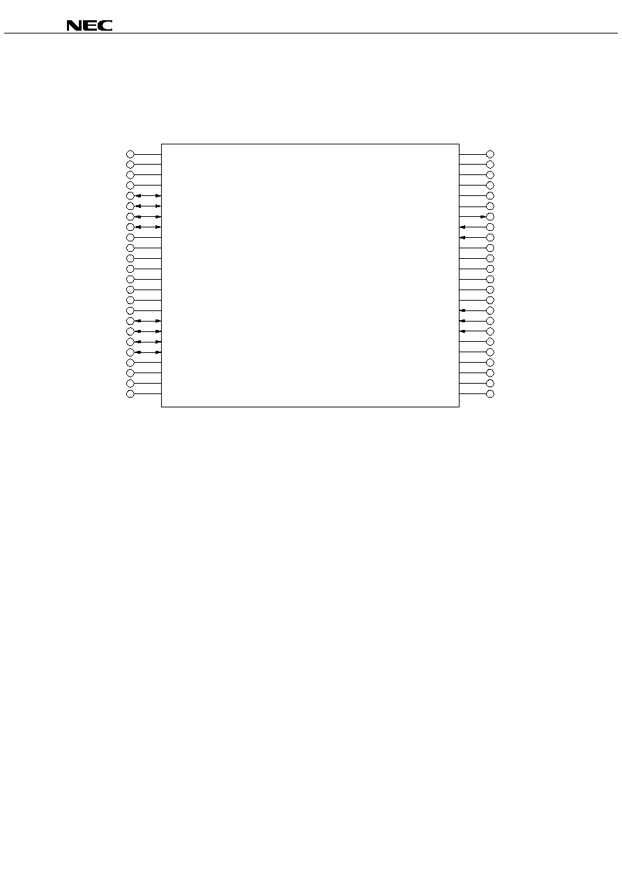
Block Diagram
I/O0
I/O1
I/O2
I/O3
I/O4
I/O5
I/O6
I/O7
/CE
CLE
ALE
/WE
/RE
Input / Output Buffer
X-Decoder
Control Logic
READ Contorol Circuit
READY/BUSY
Control Circuit
Command
Register
Address
Register
ID Register
Status Register
Dara Register Circuit
R, /B (Open-drain)
Sense Amplifier
Y-Selector
Memory Cell Matrix
Vcc
Vss