©
1996
DATA SHEET
SILICON POWER TRANSISTOR
NEL2035F03-24
NPN SILICON EPITAXIAL TRANSISTOR
L Band Power Amplifier
DESCRIPTION AND APPLICATIONS
NEL2035F03-24 of NPN epitaxial microwave power transistors
is designed for 1.8-2 GHz PHS/PCN/PCS base station applications.
It incorporates emitter ballast resistors, gold metallizations and
offers a high degree of reliability.
FEATURES
∑
High Linear Power and Gain
∑
Low Internal Modulation Distortion
∑
High Reliability Gold Metallization
∑
Emitter Ballasting
∑
24 V Operation
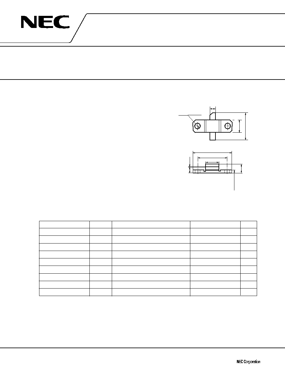
OUTLINE DIMENSIONS (Unit: mm)
ABSOLUTE MAXIMUM RATING (T
A
= 25 ∞C)
PARAMETER
SYMBOL
SPECIFIED CONDITION
RATINGS
UNIT
Collector to Base Voltage
V
CBO
45
V
Collector to Emitter Voltage
V
CER
R = 10
30
V
Emitter to Base Voltage
V
EBO
3
V
Collector to Emitter Voltage
V
CEO
18
V
Collector Current
I
C
14
A
Power Dissipation
P
T
79.5
W
Thermal Resistance
Rth(j-c)
2.2
∞C/W
Junction Temperature
Tj
200
∞C
Storage Temperature
T
stg
≠65 to 150
∞C
2.8 ±0.2
1
3
2
14.35 ±0.4
6.35 ±0.4
18.9 ±0.3
14.2 ±0.3
6.35 ±0.4
4.67 ±0.4
2.17 ±0.3
1.53 ±0.3
0.1
+0.05
≠0.02
1 - EMITTER
2 - BASE
3 - COLLECTOR
2
◊
3.3 ±0.3
Document No. P11584EJ1V0DS00 (1st edition)
Date Published June 1996 P
Printed in Japan
2
NEL2035F03-24
ELECTRICAL CHARACTERISTICS (T
A
= 25 ∞C)
PARAMETER
SYMBOL
SPECIFIED CONDITION
MIN.
TYP.
MAX.
UNIT
Collector to Emitter Cutoff
I
CES
V
CE
= 24 V
10
mA
Current
Collector to Emitter Voltage
V
CER
I
C
= 20 mA, R = 10
30
85
V
(Base to Emitter Registor = 10
)
Collector to Emitter Voltage
V
CEO
I
C
= 20 mA
18
22
V
(Open Base)
Collector to Base Voltage
V
CBO
I
C
= 20 mA
45
85
V
(Open Emitter)
Emitter to Base Voltage
V
EBO
I
C
= 25 mA
3
5.3
V
(Open Collector)
DC Forward Current Gain
h
FE
V
CE
= 5 V, I
C
= 1 A
30
100
150
Output Capacitance
C
ob
V
CE
= 24 V, f = 1 MHz
189
pF
NEL2035F03-24
3
PERFORMANCE SPECIFICATIONS (T
A
= 25 ∞C)
CLASS AB OPERATION
PARAMETER
SYMBOL
SPECIFIED CONDITION
MIN.
TYP.
MAX.
UNIT
Output Power
P
IdB
f = 1.97 GHz, Iq = 100 mA,
30
33
W
V
CC
= 24 V, CLASS AB
Collector Efficiency
c
f = 1.97 GHz, P
out
= P
IdB
, Iq = 100 mA,
40
50
%
V
CC
= 24 V, CLASS AB
Linear Gain
GL
f = 1.97 GHz, P
in
= 2 W, Iq = 100 mA,
9
dB
V
CC
= 24 V, CLASS AB
3rd Order Intermodulation
IM
3
f = 1.97 GHz,
f = 100 kHz, 30 W PEP,
≠33
dBc
V
CC
= 24 V, Iq = 100 mA, CLASS AB
CLASS A OPERATION
PARAMETER
SYMBOL
SPECIFIED CONDITION
MIN.
TYP.
MAX.
UNIT
Output Power
P
IdB
f = 1.97 GHz, Iq = 1.5 A,
7
W
V
CC
= 16 V, CLASS A
Collector Efficiency
c
f = 1.97 GHz, P
out
= P
IdB
, Iq = 1.5 A,
30
%
V
CC
= 16 V, CLASS A
Linear Gain
GL
f = 1.97 GHz, P
in
= 0.1 W, Iq = 1.5 A,
10.7
dB
V
CC
= 16 V, CLASS A
3rd Order Intermodulation
IM
3
f = 1.97 GHz,
f = 100 kHz, 5 W PEP,
≠33
dBc
V
CC
= 16 V, Iq = 1.5 A, CLASS A
4
NEL2035F03-24
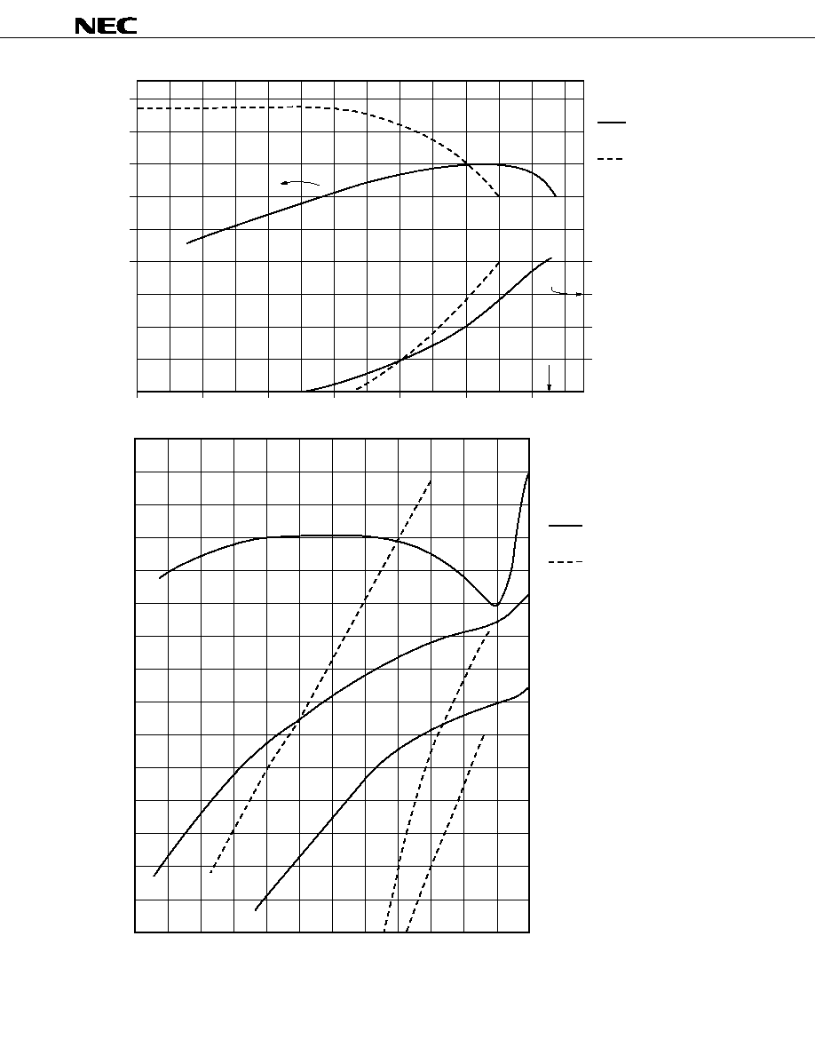
11
10
9
8
7
40
44
P
out
(dBm)
Class AB, V
cc
= 24 V
I
q
= 100 mA
Class A, V
cc
= 16 V
I
q
= 1.5 A
Gain (dB)
f = 1970 MHz
6
32
36
24
28
20
50
40
30
20
c
(%)
30 W
≠25
≠30
≠45
≠40
≠35
22
26
30
34
38
Class AB, V
cc
= 24 V
I
q
= 100 mA
Class A, V
cc
= 16 V
I
q
= 1.5 A
f1 = 1970 MHz
f2 = 1970.1 MHz
42
≠50
≠55
≠60
IM
3
IM
5
IM
7
P
out
(dBm) ∑∑∑ PEP
IM (dBc)
46

NEL2035F03-24
5
S-PARAMETER
NEL2035 Class A
V
CC
= 16 V, I
cq
= 1.5 A
FREQUENCY
S
11
S
12
S
21
S
22
GHz
MAG
ANG (DEG)
MAG
ANG (DEG)
MAG
ANG (DEG)
MAG
ANG (DEG)
1.70
0.98
165
0.04
48
0.42
73
0.92
160
1.71
0.98
165
0.04
47
0.44
71
0.91
160
1.72
0.98
165
0.04
47
0.47
68
0.90
160
1.73
0.97
164
0.04
45
0.49
65
0.89
160
1.74
0.97
164
0.04
43
0.51
62
0.88
160
1.75
0.96
164
0.04
40
0.54
59
0.87
160
1.76
0.95
163
0.04
37
0.57
57
0.86
160
1.77
0.94
163
0.04
33
0.61
53
0.85
160
1.78
0.93
163
0.04
29
0.65
48
0.84
161
1.79
0.92
162
0.04
25
0.69
43
0.82
161
1.80
0.90
162
0.04
21
0.71
37
0.81
162
1.81
0.89
162
0.05
15
0.74
32
0.80
163
1.82
0.87
163
0.05
10
0.78
26
0.79
165
1.83
0.86
163
0.05
≠1
0.81
19
0.79
166
1.84
0.85
164
0.04
≠8
0.83
11
0.79
168
1.85
0.84
165
0.04
≠14
0.84
3
0.80
170
1.86
0.83
167
0.04
≠15
0.81
≠5
0.82
171
1.87
0.84
168
0.03
≠20
0.78
≠11
0.84
172
1.88
0.84
169
0.03
≠25
0.75
≠18
0.87
172
1.89
0.85
170
0.03
≠28
0.72
≠24
0.89
172
1.90
0.86
171
0.02
≠33
0.69
≠30
0.91
172
1.91
0.87
171
0.02
≠36
0.65
≠36
0.93
172
1.92
0.89
171
0.01
≠38
0.60
≠42
0.94
171
1.93
0.90
171
0.01
≠34
0.55
≠46
0.95
171
1.94
0.90
171
0.01
≠26
0.51
≠49
0.96
170
1.95
0.91
171
0.01
≠21
0.49
≠51
0.97
169
1.96
0.92
171
0.01
≠13
0.46
≠55
0.97
169
1.97
0.93
171
0.01
≠1
0.43
≠58
0.98
168
1.98
0.93
171
0.01
16
0.40
≠61
0.98
168
1.99
0.94
171
0.01
30
0.37
≠63
0.98
167
2.00
0.94
171
0.01
38
0.35
≠65
0.99
167
NEL2035 Class AB
V
CC
= 24 V, I
cq
= 0.1 A
FREQUENCY
S
11
S
12
S
21
S
22
GHz
MAG
ANG (DEG)
MAG
ANG (DEG)
MAG
ANG (DEG)
MAG
ANG (DEG)
1.70
0.98
167
0.04
68
0.20
90
0.95
156
1.71
0.98
167
0.04
65
0.22
88
0.95
155
1.72
0.98
167
0.04
63
0.23
86
0.94
155
1.73
0.98
166
0.04
61
0.25
84
0.93
154
1.74
0.98
166
0.04
60
0.26
82
0.92
154
1.75
0.97
166
0.05
59
0.28
80
0.92
153
1.76
0.97
166
0.05
56
0.30
79
0.90
152
1.77
0.97
165
0.05
53
0.33
76
0.89
151
1.78
0.97
165
0.05
51
0.36
72
0.87
150
1.79
0.96
165
0.06
48
0.38
68
0.85
149
1.80
0.96
164
0.06
45
0.42
65
0.82
147
1.81
0.95
164
0.07
41
0.45
60
0.78
146
1.82
0.94
164
0.07
35
0.51
55
0.74
145
1.83
0.93
164
0.08
31
0.56
49
0.68
144
1.84
0.92
163
0.08
23
0.62
41
0.62
145
1.85
0.90
163
0.08
15
0.67
32
0.55
148
1.86
0.88
164
0.08
4
0.71
21
0.49
155
1.87
0.87
165
0.08
≠7
0.73
10
0.47
165
1.88
0.86
166
0.08
≠18
0.74
≠1
0.49
56
1.89
0.86
167
0.07
≠29
0.72
≠13
0.56
≠56
1.90
0.87
169
0.06
≠39
0.68
≠23
0.64
≠173
1.91
0.88
169
0.05
≠48
0.63
≠33
0.72
≠173
1.92
0.89
170
0.05
≠56
0.57
≠42
0.78
≠174
1.93
0.90
170
0.04
≠62
0.51
≠49
0.83
≠176
1.94
0.91
170
0.03
≠67
0.46
≠54
0.86
≠58
1.95
0.92
170
0.03
≠71
0.42
≠58
0.89
60
1.96
0.93
170
0.02
≠74
0.39
≠63
0.91
178
1.97
0.93
170
0.02
≠77
0.35
≠67
0.92
177
1.98
0.94
170
0.02
≠80
0.32
≠70
0.93
175
1.99
0.94
169
0.01
≠84
0.30
≠73
0.94
174
2.00
0.95
169
0.01
≠89
0.27
≠76
0.95
173
6
NEL2035F03-24
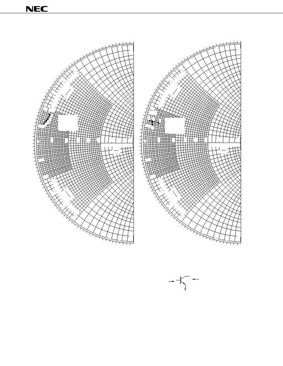
NEL2035F03-24 Z
in
/Z
out
0.1
0.2
0.3
0.4
0.5
0.6
0.7
0.8
0.9
1.0
1.2
1.4
1.6
1.8
2.0
3.0
4.0
5.0
10
20
50
0.1
0.2
0.3
0.4
0.5
0.6
0.7
0.8
0.9
1.0
1.2
1.4
1.6
1.8
2.0
3.0
4.0
5.0
10
20
50
0.2
0.1
0.3
0.4
0.5
0
0.6
0.7
0.8
0.9
1.0
1.2
1.4
1.6
1.8
2.0
3.0
4.0
5.0
10
20
50
0.2
0.4
0.6
0.8
1.0
0.2
0.4
0.6
0.8
1.0
0.2
0.4
0.6
0.8
1.0
0.2
0.4
0.6
0.8
1.0
RESISTANCE COMPONENT
R
Zo
PO
SI
TI
VE
RE
AC
TA
NC
E
CO
MP
ON
EN
T
NE
GA
TIV
E
RE
AC
TA
NC
E
CO
M
PO
NE
NT
≠JX
Zo
+JX
Zo
Z
in
2
3
4
1
1: 1.8 GHz
2: 1.9
3: 1.97
4: 2.0
Z
O
= 50 ohm
f [GHz]
1.80
1.90
1.97
2.00
Z
in
[ohm]
2.6 + j8.4
2.3 + j7.0
2.3 + j6.5
1.6 + j5.6
Z
out
[ohm]
4.6 + j5.8
2.0 + j5.2
2.3 + j6.0
1.3 + j6.2
Z
in
Z
out
0.1
0.2
0.3
0.4
0.5
0.6
0.7
0.8
0.9
1.0
0.1
0.2
0.3
0.4
0.5
0.6
0.7
0.8
0.9
1.0
0.2
0.1
0.3
0.4
0.5
0
0.6
0.7
0.8
0.9
1.0
2
0
0
2
RESISTANCE COMPONENT
R
Zo
PO
SI
TI
VE
RE
AC
TA
NC
E
CO
MP
ON
EN
T
NE
GA
TIV
E
RE
AC
TA
NC
E
CO
M
PO
NE
NT
≠JX
Zo
+JX
Zo
Z
out
2
3
4
1
1: 1.8 GHz
2: 1.9
3: 1.97
4: 2.0
NEL2035F03-24
7
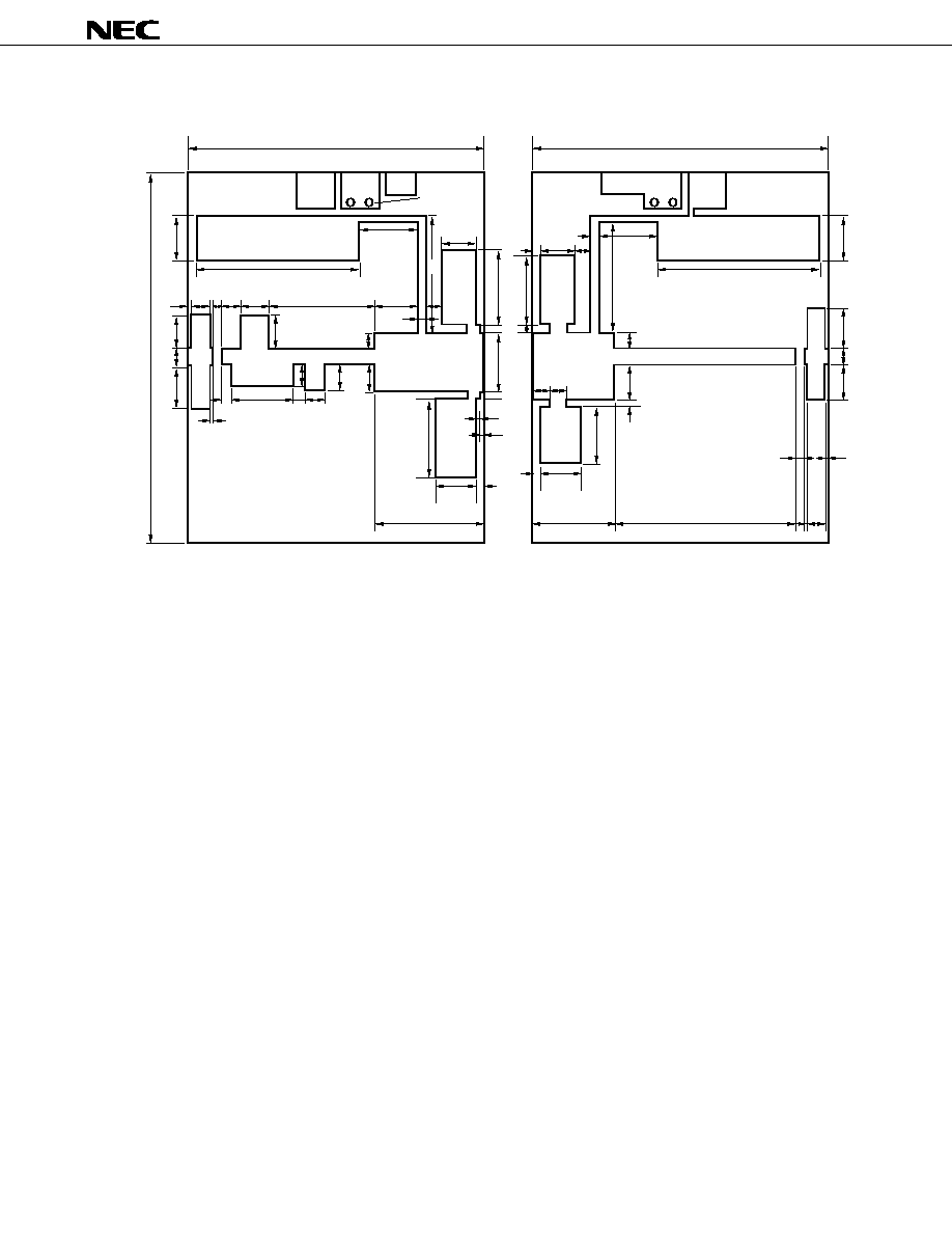
Circuit Drawing
,,,
,,,,,
,,,,,,,
,,,,,,,,,
,,,,,,,,,,
,,,,,,,,,
,,,,,,,
,,,,,
,,,
,,
,,,
,,
,,
,,,,
,,
,
,,
,,
,,,
,,
,
,,,
,,,,,
,,,,,,,
,,,,,,,,,
,,,,,,,,,,
,,,,,,,,,,
,,,,,,,,
,,,,,,
,,,,
,,
,,,
,,,
,,
input
output
40 mm
8
Thru hole
1 mm
◊
4
2.2 1 2.8 3.9
14.6
6
5
1
4.8
2
6
0.5
5
5.8
2.3
22
16
2
10.5
7.6
1
1
1
9.5
3.3
3.1
2.1
6
15
1
8.8
1.5 2.8
1
0.3
50 mm
0.5
0.5
10
40 mm
1
6
1
8
4.5
1
1.8
5
2
8
1
15
22
6
25.5
10.5
2
0.9
1
0.1
4
3.3
2.3
1
µ
SUBSTRATE (TEFLON)
DICLAD522TÆ
THICKNESS = 0.79 mm
DOUBLE SIDE 35 m Cu
r = 2.60
2.5
2.5
8
NEL2035F03-24
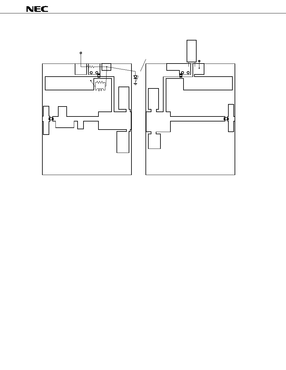
Components Layout
input
output
C1
L1
C2
R2
V
BB
C3
C5
C4
V
CC
This lead is
placed near
device flange
D1
≠
R1
:
:
:
:
:
R1
R2
L1
C1, C2, C3, C5: MURATA 47 pF
C4
D1
5.1
30
5 mm 10T
22 F (50 V)
Electrolytic Capacitor
V06C
µ
NEL2035F03-24
9
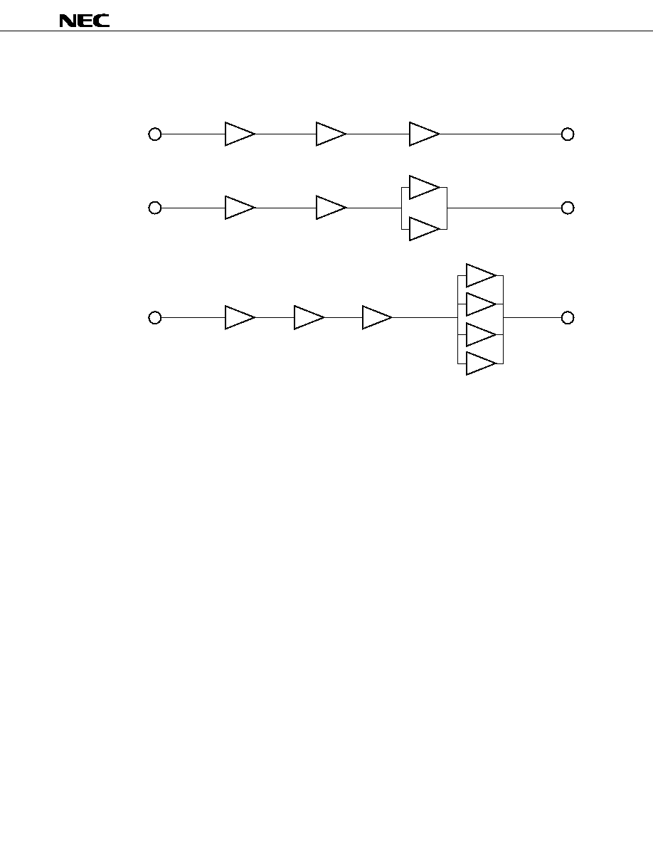
APPLICATION
= Amplifier Diagrams =
95 mW
40 mW
NEL2001
NEL2004
NEL2012
NEL2012
NEL2035
NEL2035
◊
2
NEL2035
◊
4
50 W
100 W
46 mW
NEL2001
NEL2012
NEL2035
30 W

10
NEL2035F03-24
[MEMO]

NEL2035F03-24
11
[MEMO]
NEL2035F03-24
No part of this document may be copied or reproduced in any form or by any means without the prior written
consent of NEC Corporation. NEC Corporation assumes no responsibility for any errors which may appear in
this document.
NEC Corporation does not assume any liability for infringement of patents, copyrights or other intellectual property
rights of third parties by or arising from use of a device described herein or any other liability arising from use
of such device. No license, either express, implied or otherwise, is granted under any patents, copyrights or other
intellectual property rights of NEC Corporation or others.
While NEC Corporation has been making continuous effort to enhance the reliability of its semiconductor devices,
the possibility of defects cannot be eliminated entirely. To minimize risks of damage or injury to persons or
property arising from a defect in an NEC semiconductor device, customers must incorporate sufficient safety
measures in its design, such as redundancy, fire-containment, and anti-failure features.
NEC devices are classified into the following three quality grades:
"Standard", "Special", and "Specific". The Specific quality grade applies only to devices developed based on a
customer designated "quality assurance program" for a specific application. The recommended applications of
a device depend on its quality grade, as indicated below. Customers must check the quality grade of each device
before using it in a particular application.
Standard: Computers, office equipment, communications equipment, test and measurement equipment,
audio and visual equipment, home electronic appliances, machine tools, personal electronic
equipment and industrial robots
Special:
Transportation equipment (automobiles, trains, ships, etc.), traffic control systems, anti-disaster
systems, anti-crime systems, safety equipment and medical equipment (not specifically designed
for life support)
Specific:
Aircrafts, aerospace equipment, submersible repeaters, nuclear reactor control systems, life
support systems or medical equipment for life support, etc.
The quality grade of NEC devices is "Standard" unless otherwise specified in NEC's Data Sheets or Data Books.
If customers intend to use NEC devices for applications other than those specified for Standard quality grade,
they should contact an NEC sales representative in advance.
Anti-radioactive design is not implemented in this product.
M4 96.5