 | –≠–ª–µ–∫—Ç—Ä–æ–Ω–Ω—ã–π –∫–æ–º–ø–æ–Ω–µ–Ω—Ç: PS9117-A | –°–∫–∞—á–∞—Ç—å:  PDF PDF  ZIP ZIP |

PS9117
NEC's HIGH CMR, 10Mbps
OPEN COLLECTOR OUTPUT TYPE
5-PIN SOP OPTOCOUPLER
California Eastern Laboratories
∑
PULSE WIDTH DISTORTION:
|t
PHL
- t
PLH
| = 35 ns MAX.
∑ HIGH COMMON MODE TRANSIENT IMMUNITY:
CM
H
, CM
L
= ±15 kV/s MIN.
∑
SMALL PACKAGE:
5-Pin SOP
∑
HIGH SPEED:
10 Mbps
∑
HIGH ISOLATION VOLTAGE:
BV = 2 500 V
r.m.s.
∑
OPEN COLLECTOR OUTPUT
∑
ORDERING NUMBER OF TAPING PRODUCT:
PS9117-F3, F4: 2 500 pcs/reel
∑
Pb-Free Product
∑
SAFETY STANDARDS:
UL approved: File No. E72422
DIN EN60747-5-2 (VDE0884 Part2) approved No. 40008902 (option)
FEATURES
DATA SHEET
NEC's PS9117 is an optically coupled high-speed,
active low type isolator containing a GaAlAs LED on
the input side and a photodiode and a signal process-
ing circuit on the output side on one chip.
The PS9117 is designed specifically for high common
mode transient immunity (CMR) and low pulse width
distortion. The PS9117 is suitable for high density ap-
plication.
DESCRIPTION
∑
Measurement Equipment
∑
PDP
∑
FA Network
APPLICATION
5
3
1
2
4
1. Anode
2. Cathode
3. GND
4. V
O
5. V
CC
PIN CONNECTION
(Top View)
TRUTH TABLE
LED
OUTPUT
ON
L
OFF
H

PS9117
PACKAGE DIMENSIONS (UNIT: mm)
1.27
0.4
+0.10
-0.05
0.25 M
0.1±0.1
2.6±0.2
4.4
7.0±0.3
0.5±0.3
0.15
+0.10 -0.0
5
3.4
+0.3
-0.1
5
3
1
2
4
MARKING EXAMPLE
No. 1 pin Mark
Initial of NEC
(Engraved mark)
Rank Code
Year Assembled
(Last 1 Digit)
Week Assembled
N 2 34
Assembly Lot
9117
N234
N
*1
*1 Bar : Pb-Free

PS9117
ORDERING INFORMATION
*1 For the application of the Safety Standard, following part number should be used.
*2 With regards to terminal solder (the solder contains lead) plated products (conventionally plated), contact your
nearby sales office.
PART NUMBER
ORDER NUMBER SOLDER PLATING
SPECIFICATION
PACKING STYLE
SAFETY
STANDARDS
APPROVAL
APPLICATION
PART NUMBER
*1
PS9117
PS9117-A
Pb-Free
*2
Magazine case 100 pcs
UL approved
PS9117
PS9117-F3
PS9117-F3-A
Embossed Tape 2 500 pcs/reel
PS9117-F4
PS9117-F4-A
PS9117-V
PS9117-V-A
Magazine case 100 pcs
DIN EN60747-5-2
(VDE0884 Part2)
Approved (Option)
PS9117-V-F3
PS9117-V-F3-A
Embossed Tape 2 500 pcs/reel
PS9117-V-F4
PS9117-V-F4-A
ABSOLUTE MAXIMUM RATINGS
(T
A
= 25∫C, unless otherwise Specified)
PARAMETER
SYMBOL
RATINGS
UNIT
Diode
Forward Current
*1
I
F
30
mA
Reverse Voltage
V
R
5
V
Detector
Supply Voltage
V
CC
7
V
Output Voltage
V
O
7
V
Output Current
I
O
25
mA
Power Dissipation
*2
P
C
40
mW
Isolation Voltage
*3
BV
2 500
Vr.m.s.
Operating Ambient Temperature
T
A
-
40 to +85
∞
C
Storage Temperature
T
stg
-
55 to +125
∞
C
*1 Reduced to 0.3 mA/∞C at T
A
= 25∞C or more.
*2 Applies to output pin V
O
(collector pin). Reduced to 1.5 mW/∞C at T
A
= 65∞C or more.
*3 AC voltage for 1 minute at T
A
= 25∞C, RH = 60% between input and output.

PS9117
RECOMMENDED OPERATING CONDITIONS
PARAMETER
SYMBOL
MIN.
TYP.
MAX.
UNIT
Low Level Input Voltage
V
FL
0
0.8
V
High Level Input Current
I
FH
6.3
10
12.5
mA
Supply Voltage
V
CC
4.5
5.0
5.5
V
TTL (R
L
= 1 k, loads)
N
5
Pull-up Resistor
R
L
330
4 k
ELECTRICAL CHARACTERISTICS
(T
A
= -40 to 85∫C, unless otherwise specified)
PARAMETER
SYMBOL
CONDITIONS
MIN.
TYP.
*1
MAX.
UNIT
Diode
Forward Voltage
V
F
I
F
= 10 mA, T
A
= 25∞C
1.4
1.65
1.8
V
Reverse Current
I
R
V
R
= 3 V, T
A
= 25∞C
10
A
Terminal Capacitance
C
t
V = 0 V, f = 1 MHz, T
A
= 25∞C
30
pF
Detector High Level Output Current
I
OH
V
CC
= V
O
= 5.5 V, V
F
= 0.8 V
1
100
A
Low Level Output Voltage
*2
V
OL
V
CC
= 5.5 V, I
F
= 5 mA, I
OL
= 13 mA
0.2
0.6
V
High Level Supply Current
I
CCH
V
CC
= 5.5 V, I
F
= 0 mA
5
8
mA
Low Level Supply Current
I
CCL
V
CC
= 5.5 V, I
F
= 10 mA
9
11
Coupled Threshold Input Current
(H L)
I
FHL
V
CC
= 5 V, V
O
= 0.8 V, R
L
= 350
2
5
Isolation Resistance
R
I-O
V
I-O
= 1 kV
DC
, RH = 40 to 60%,
T
A
= 25∞C
10
11
Isolation Capacitance
C
I-O
V = 0 V, f = 1 MHz, T
A
= 25∞C
0.6
pF
Propagation Delay Time
(H L)
*3
t
PHL
T
A
= 25∞C
35
75
ns
V
CC
= 5 V, R
L
= 350 , I
F
= 7.5 mA
100
Propagation Delay Time
(L H)
*3
t
PLH
T
A
= 25∞C
40
75
V
CC
= 5 V, R
L
= 350 , I
F
= 7.5 mA
100
Rise Time
t
r
V
CC
= 5 V, R
L
= 350 , I
F
= 7.5 mA
20
Fall Time
t
f
5
Pulse Width Distortion (PWD)
*3
|t
PHL-
t
PLH
|
5
35
Propagation Delay Skew
t
PSK
40
Common Mode
Transient Immunity at High
Level Output
*4
CM
H
V
CC
= 5 V, R
L
= 350 , T
A
= 25∞C,
I
F
= 0 mA, V
O
> 2 V, V
CM
= 1 kV
15
20
kV/s
Common Mode
Transient Immunity at Low Level
Output
*4
CM
L
V
CC
= 5 V, R
L
= 350 , T
A
= 25∞C,
I
F
= 7.5 mA, V
O
< 0.8 V, V
CM
= 1 kV
15
20
kV/s
PS9117
*1 Typical values at T
A
= 25∞C
*2 Because V
OL
of 2 V or more may be output when LED current input and when output supply of V
CC
= 2.6 V or less, it is
important to confirm the characteristics (operation with the power supply on and off) during design, before using this device.
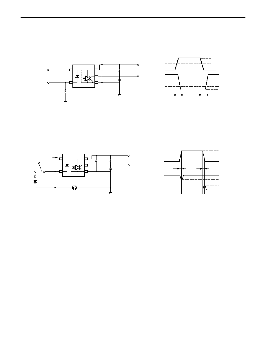
*3 Test circuit for propagation delay time
Input
Output
1.5 V
V
OL
t
PHL
t
PLH
(I
F
= 7.5 mA)
50%
47
Pulse input (I
F
)
V
O
(monitor)
V
CC
= 5 V
Input
(monitor)
0.1 F
µ
C
L
= 15 pF
R
L
= 350
(PW = 1 s,
Duty cycle = 1/10)
µ
Remark C
L
includes probe and stray wiring capacitance.
*4 Test circuit for common mode transient immunity
90%
10%
1 kV
0 V
V
OH
2 V
0.8 V
V
OL
V
CM
V
O
(I
F
= 0 mA)
V
O
(I
F
= 7.5 mA)
t
r
t
f
V
O
(monitor)
V
CC
= 5 V
0.1 F
µ
C
L
= 15 pF
SW
V
CM
I
F
R
L
= 350
Remark C
L
includes probe and stray wiring capacitance.
USAGE CAUTIONS
1. This product is weak for static electricity by designed with high-speed integrated circuit so protect against static electricity
when handling.
2. By-pass capacitor of 0.1 F is used between V
CC
and GND near device. Also, ensure that the distance between the leads of
the photocoupler and capacitor is no more than 10 mm.