Document Outline
- COVER
- FEATURES
- APPLICATIONS
- ORDERING INFORMATION
- PIN CONFIGURATION (TOP VIEW)
- PIN NAMES
- INTERNAL BLOCK DIAGRAM
- 1. DIFFERENCES BETWEEN V850E/MS2 AND V850E/MS1
- 2. PIN FUNCTIONS
- 2.1 Port Pins
- 2.2 Non-Port Pins
- 2.3 Pin I/O Circuits and Recommended Connection of Unused Pins
- 3. ELECTRICAL SPECIFICATIONS
- 4. PACKAGE DRAWING
- 5. RECOMMENDED SOLDERING CONDITIONS
MOS INTEGRATED CIRCUIT
µ
µ
µ
µ
PD703130
V850E/MS2
TM
32-BIT SINGLE-CHIP MICROCONTROLLER
Document No. U15390EJ1V0DS00 (1st edition)
Date Published April 2001 N CP(K)
Printed in Japan
PRELIMINARY DATA SHEET
The
µPD703130 is a member of the V850 Family
TM
of 32-bit single-chip microcontrollers designed for real-time
control operations. These microcontrollers provide on-chip features, including a 32-bit CPU, RAM, interrupt
controller, real-time pulse unit, serial interface, A/D converter, and DMA controller.
The
µPD703130 is a ROMless version product.
Detailed function descriptions are provided in the following user's manuals. Be sure to read them before
designing.
V850E/MS2 User's Manual Hardware:
U14985E
V850E/MS1
TM
User's Manual Architecture: U12197E
FEATURES
∑ Number of instructions: 81
∑ Minimum instruction execution time 30 ns (@ 33 MHz operation)
∑ General-purpose registers 32 bits
◊ 32
∑ Instruction set suitable for control applications
∑ Internal memory ROM: None
RAM: 4 KB
∑ Advanced on-chip interrupt controller
∑ Real-time pulse unit suitable for control operations
∑ Powerful serial interface (on-chip dedicated baud rate generator)
∑ On-chip clock generator
∑ 10-bit resolution A/D converter: 4 channels
∑ DMA controller: 4 channels
∑ Power saving functions
APPLICATIONS
∑ Optical storage equipment (DVD players, etc.)
∑ System control for digital consumer equipment, etc.
©
2001
The information contained in this document is being issued in advance of the production cycle for the
device. The parameters for the device may change before final production or NEC Corporation, at its own
discretion, may withdraw the device prior to its production.
Not all devices/types available in every country. Please check with local NEC representative for
availability and additional information.
Preliminary Data Sheet U15390EJ1V0DS
2
µ
µ
µ
µ
PD703130
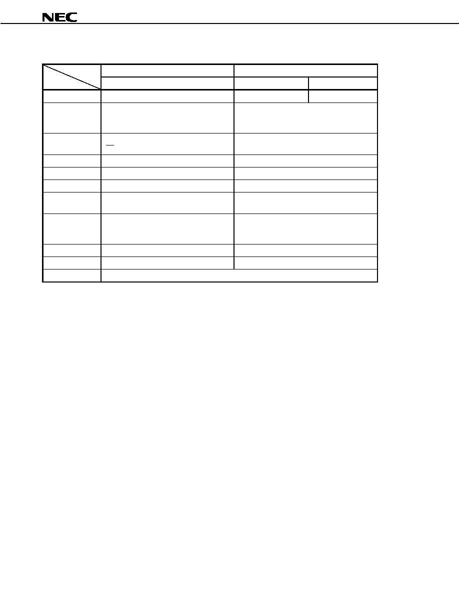
ORDERING INFORMATION
Part Number
Package
Maximum Operating
Frequency
Internal ROM
µPD703130GC-8EU
100-pin plastic LQFP (fine pitch) (14
◊ 14)
33 MHz
None
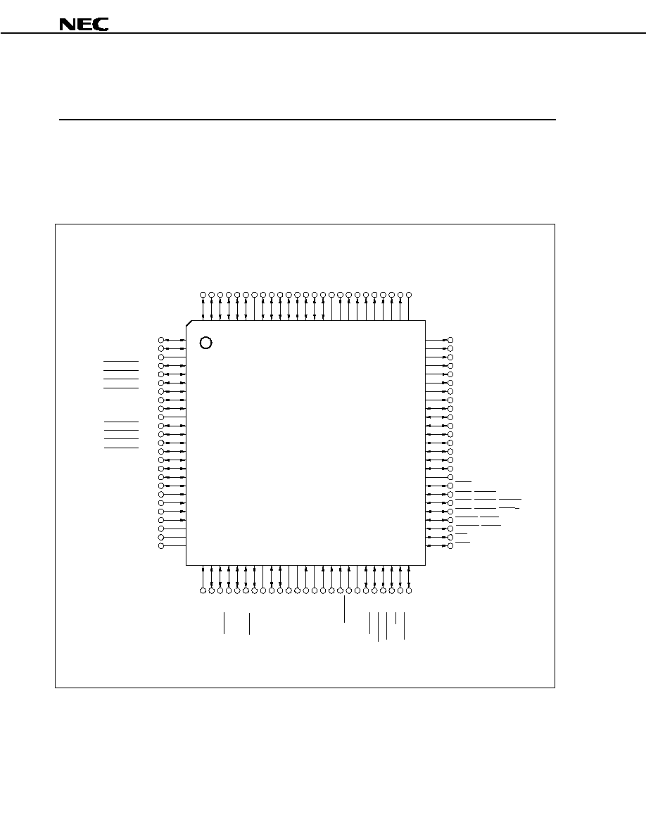
PIN CONFIGURATION (TOP VIEW)
100-pin plastic LQFP (fine pitch) (14
◊
◊
◊
◊ 14)
∑
µPD703130GC-8EU
1
2
3
4
5
6
7
8
9
10
11
12
13
14
15
16
17
18
19
20
21
22
23
24
25
D1
D0
V
DD
INTP103/DMARQ3/P07
INTP102/DMARQ2/P06
INTP101/DMARQ1/P05
INTP100/DMARQ0/P04
TCLR10/P02
TO100/P00
V
SS
INTP113/DMAAK3/P17
INTP112/DMAAK2/P16
INTP111/DMAAK1/P15
INTP110/DMAAK0/P14
TCLR11/P12
TO110/P10
TCLR12/P102
TO120/P100
ANI3/P73
ANI2/P72
ANI1/P71
ANI0/P70
AV
DD
AV
SS
AV
REF
A8
A9
A10
A11
A12
A13
A14
A15
A16/P60
A17/P61
A18/P62
A19/P63
A20/P64
A21/P65
A22/P66
A23/P67
HV
DD
CS0/P80
CS3/RAS3/P83
CS4/RAS4/IOWR/P84
CS5/RAS5/IORD/P85
LCAS/LWR/P90
UCAS/UWR/P91
RD/P92
WE/P93
NMI/P20
TXD0/SO0/P22
RXD0/SI0/P23
SCK0/P24
TXD1/SO1/P25
RXD1/SI1/P26
SCK1/P27
V
DD
INTP130/P34
TI13/P33
CV
DD
X2
X1
CV
SS
CKSEL
MODE0
MODE2
RESET
V
SS
CLKOUT/PX7
WAIT/PX6
HLDRQ/P97
HLDAK/P96
OE/P95
BCYST/P94
D2
D3
D4
D5
D6
D7
V
SS
D8/P50
D9/P51
D10/P52
D11/P53
D12/P54
D13/P55
D14/P56
D15/P57
HV
DD
A0
A1
A2
A3
A4
A5
A6
A7
V
SS
75
74
73
72
71
70
69
68
67
66
65
64
63
62
61
60
59
58
57
56
55
54
53
52
51
100
99
98
97
96
95
94
93
92
91
90
89
88
87
86
85
84
83
82
81
80
79
78
77
76
26
27
28
29
30
31
32
33
34
35
36
37
38
39
40
41
42
43
44
45
46
47
48
49
50
Preliminary Data Sheet U15390EJ1V0DS
3
µ
µ
µ
µ
PD703130
PIN NAMES
A0 to A23:
Address bus
P20, P22 to P27:
Port 2
ANI0 to ANI3:
Analog input
P33, P34:
Port 3
AV
DD
:
Analog power supply
P50 to P57:
Port 5
AV
REF
:
Analog reference voltage
P60 to P67:
Port 6
AV
SS
:
Analog ground
P70 to P73:
Port 7
BCYST:
Bus cycle start timing
P80, P83 to P85:
Port 8
CKSEL:
Clock generator operating mode select
P90 to P97:
Port 9
CLKOUT:
Clock output
P100, P102:
Port 10
CS0, CS3 to CS5:
Chip select
PX6, PX7:
Port X
CV
DD
:
Clock generator power supply
RAS3 to RAS5:
Row address strobe
CV
SS
:
Clock generator ground
RD:
Read
D0 to D15:
Data bus
RESET:
Reset
DMAAK0 to DMAAK3: DMA acknowledge
RXD0, RXD1:
Receive data
DMARQ0 to DMARQ3: DMA request
SCK0, SCK1:
Serial clock
HLDAK:
Hold acknowledge
SI0, SI1:
Serial input
HLDRQ:
Hold request
SO0, SO1:
Serial output
HV
DD
:
Power supply for external pins
TCLR10 to TCLR12: Timer clear
INTP100 to INTP103, : Interrupt request from peripherals
TI13:
Timer input
INTP110 to INTP113,
TO100, TO110:
Timer output
INTP130
TO120
IORD:
I/O read strobe
TXD0, TXD1:
Transmit data
IOWR:
I/O write strobe
UCAS:
Upper column address strobe
LCAS:
Lower column address strobe
UWR:
Upper write strobe
LWR:
Lower write strobe
V
DD
:
Power supply for internal unit
MODE0, MODE2:
Mode
V
SS
:
Ground
NMI:
Non-maskable interrupt request
WAIT:
Wait
OE:
Output enable
WE:
Write enable
P00, P02, P04 to P07: Port 0
X1, X2:
Crystal
P10, P12, P14 to P17: Port 1
Preliminary Data Sheet U15390EJ1V0DS
4
µ
µ
µ
µ
PD703130
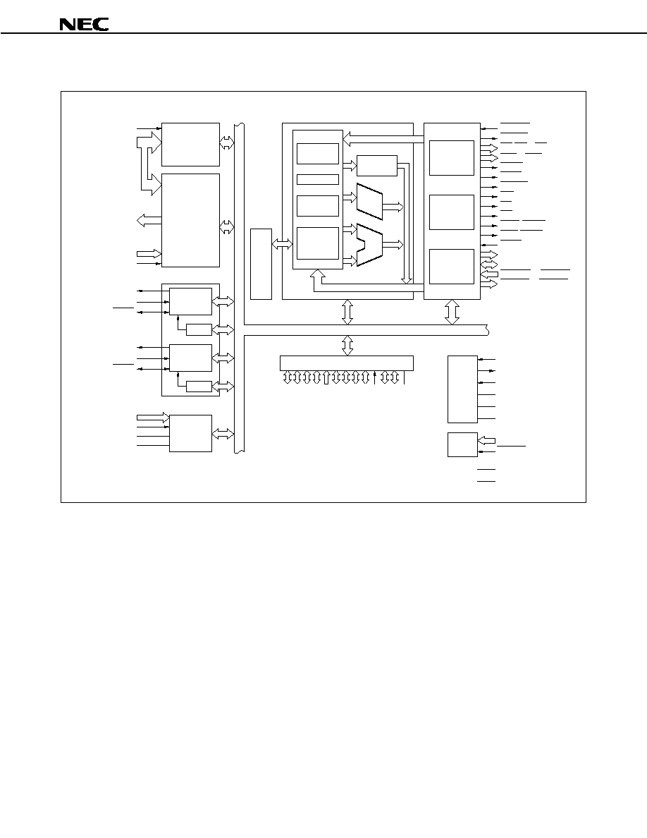
INTERNAL BLOCK DIAGRAM
HLDRQ
HLDAK
CS0,CS3 to CS5
RAS3 to RAS5
IOWR
IORD
BCYST
WE
RD
OE
UWR/UCAS
LWR/LCAS
WAIT
A0 to A23
D0 to D15
DMARQ0 to DMARQ3
DMAAK0 to DMAAK3
NMI
TO100,TO110,
TO120
INTP100 to INTP103
INTP110 to INTP113
INTP130
TCLR10 to TCLR12
TI13
INTC
RPU
SIO
RAM
4 KB
CPU
PC
Instruction
queue
System
registers
General-purpose
registers
(32 bits
◊
32)
ALU
Multiplier
(32
◊
32
64)
Barrel
shifter
Port
PX6,PX7
P100,P102
P90 to P97
P80,P83 to P85
P70 to P73
P60 to P67
P50 to P57
P33,P34
P22 to P27
P20
P10,P12,P14 to P17
P00,P02,P04 to P07
HV
DD
CG
System
controller
BCU
CLKOUT
CKSEL
X1
X2
CV
DD
CV
SS
MODE0,MODE2
RESET
UART0/CSI0
BRG0
UART1/CSI1
BRG1
ADC
SO0/TXD0
SI0/RXD0
SCK0
SO1/TXD1
SI1/RXD1
SCK1
ANI0 to ANI3
AV
REF
AV
SS
AV
DD
V
DD
V
SS
DMAC
PageROM
controller
DRAMC

Preliminary Data Sheet U15390EJ1V0DS
5
µ
µ
µ
µ
PD703130
CONTENTS
1.
DIFFERENCES BETWEEN V850E/MS2 AND V850E/MS1............................................................
6
2.
PIN FUNCTIONS .............................................................................................................................
7
2.1
Port Pins .................................................................................................................................
7
2.2
Non-Port Pins .........................................................................................................................
9
2.3
Pin I/O Circuits and Recommended Connection of Unused Pins..................................... 11
3.
ELECTRICAL SPECIFICATIONS ................................................................................................... 14
4.
PACKAGE DRAWING ..................................................................................................................... 68
5.
RECOMMENDED SOLDERING CONDITIONS............................................................................. 69
Preliminary Data Sheet U15390EJ1V0DS
6
µ
µ
µ
µ
PD703130
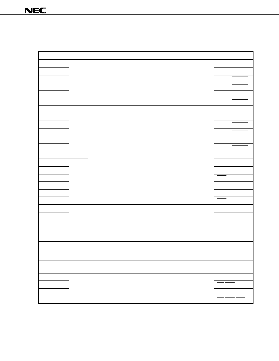
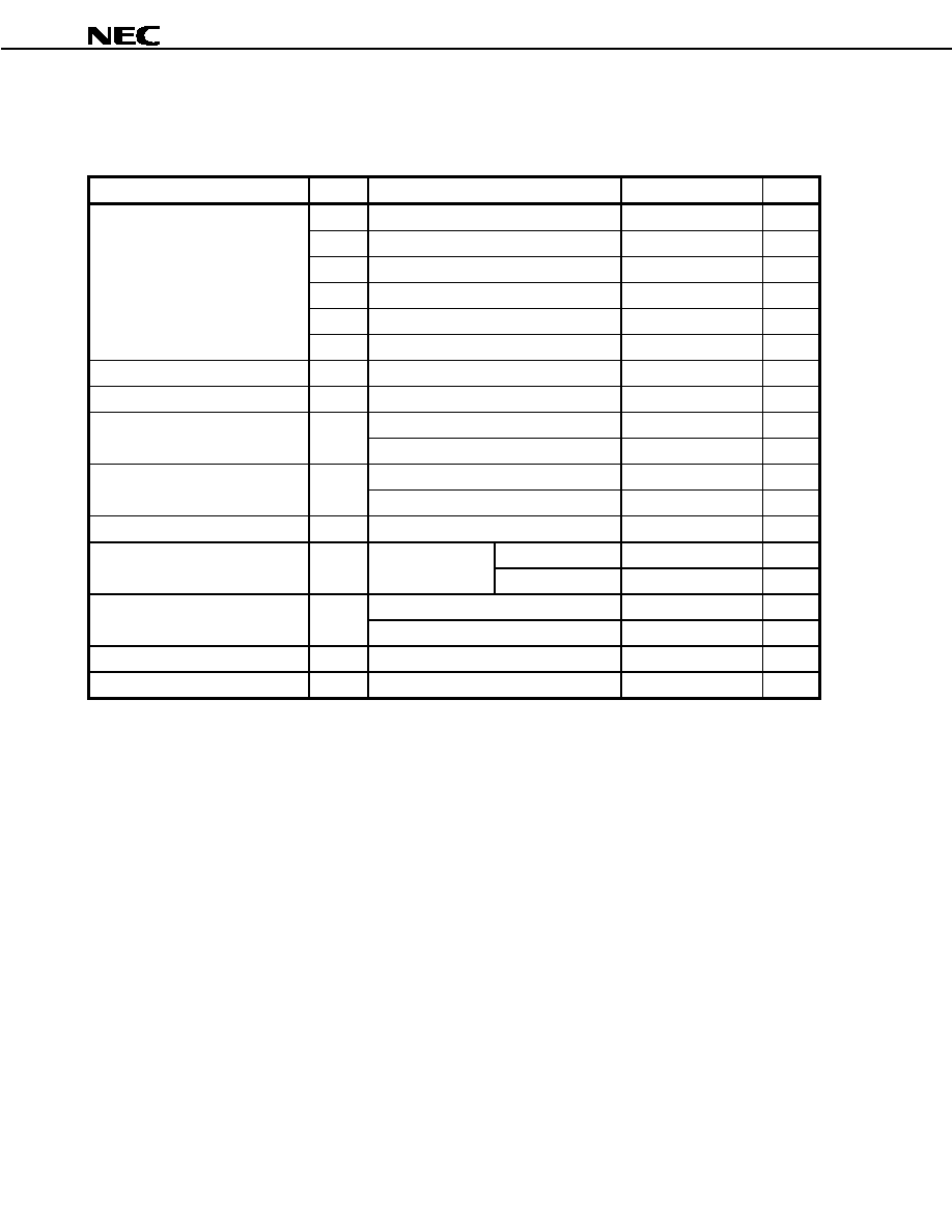
1. DIFFERENCES BETWEEN V850E/MS2 AND V850E/MS1
Product Name
V850E/MS2
V850E/MS1
Item
µPD703130
µPD703100-33
µPD703102-33
Internal ROM
None
None
128 KB (mask ROM)
Maximum
operating
frequency
33 MHz
33 MHz
Memory space
64 MB linear (only 22 MB supports on-chip
CS signal)
64 MB linear
Chip select output
4 spaces
8 spaces
Interrupt function
External: 10, internal: 35
External: 25, internal: 47
I/O lines
Input: 5, I/O: 52
Input: 9, I/O: 114
Timer
16-bit timer/event counter: 4 channels
16-bit timer: 2 channels
16-bit timer/event counter: 6 channels
16-bit timer: 2 channels
Serial interface
CSI/UART: 2 channels
Dedicated baud rate generator: 2 channels
CSI: 2 channels
CSI/UART: 2 channels
Dedicated baud rate generator: 3 channels
A/D converter
10-bit resolution
◊ 4 channels
10-bit resolution
◊ 8 channels
Package
100-pin plastic LQFP (fine-pitch) (14
◊ 14)
144-pin plastic LQFP (fine-pitch) (20
◊ 20)
Other
Noise tolerance and noise radiation will differ due to differences in circuit scale and mask layout.
Preliminary Data Sheet U15390EJ1V0DS
7
µ
µ
µ
µ
PD703130
2. PIN FUNCTIONS
2.1 Port Pins
(1/2)
Pin Name
I/O
Function
Alternate Function
P00
TO100
P02
TCLR10
P04
INTP100/DMARQ0
P05
INTP101/DMARQ1
P06
INTP102/DMARQ2
P07
I/O
Port 0
6-bit I/O port
Input/output can be specified in 1-bit units.
INTP103/DMARQ3
P10
TO110
P12
TCLR11
P14
INTP110/DMAAK0
P15
INTP111/DMAAK1
P16
INTP112/DMAAK2
P17
I/O
Port 1
6-bit I/O port
Input/output can be specified in 1-bit units.
INTP113/DMAAK3
P20
Input
NMI
P22
TXD0/SO0
P23
RXD0/SI0
P24
SCK0
P25
TXD1/SO1
P26
RXD1/SI1
P27
I/O
Port 2
P20 is an input only port.
When a valid edge is input, this pin operates as NMI input. Also, bit 0
of the P2 register indicates the NMI input status.
P22 to P27 are 6-bit I/O port.
Input/output can be specified in 1-bit units.
SCK1
P33
TI13
P34
I/O
Port 3
2-bit I/O port
Input/output can be specified in 1-bit units.
INTP130
P50 to P57
I/O
Port 5
8-bit I/O port
Input/output can be specified in 1-bit units.
D8 to D15
P60 to P67
I/O
Port 6
8-bit I/O port
Input/output can be specified in 1-bit units.
A16 to A23
P70 to P73
Input
Port 7
4-bit input only port
ANI0 to ANI3
P80
CS0
P83
CS3/RAS3
P84
CS4/RAS4/IOWR
P85
I/O
Port 8
4-bit I/O port
Input/output can be specified in 1-bit units.
CS5/RAS5/IORD
Preliminary Data Sheet U15390EJ1V0DS
8
µ
µ
µ
µ
PD703130
(2/2)
Pin Name
I/O
Function
Alternate Function
P90
LCAS/LWR
P91
UCAS/UWR
P92
RD
P93
WE
P94
BCYST
P95
OE
P96
HLDAK
P97
I/O
Port 9
8-bit I/O port
Input/output can be specified in 1-bit units.
HLDRQ
P100
TO120
P102
I/O
Port 10
2-bit I/O port
Input/output can be specified in 1-bit units.
TCLR12
PX6
WAIT
PX7
I/O
Port X
2-bit I/O port
Input/output can be specified in 1-bit units.
CLKOUT
Preliminary Data Sheet U15390EJ1V0DS
9
µ
µ
µ
µ
PD703130
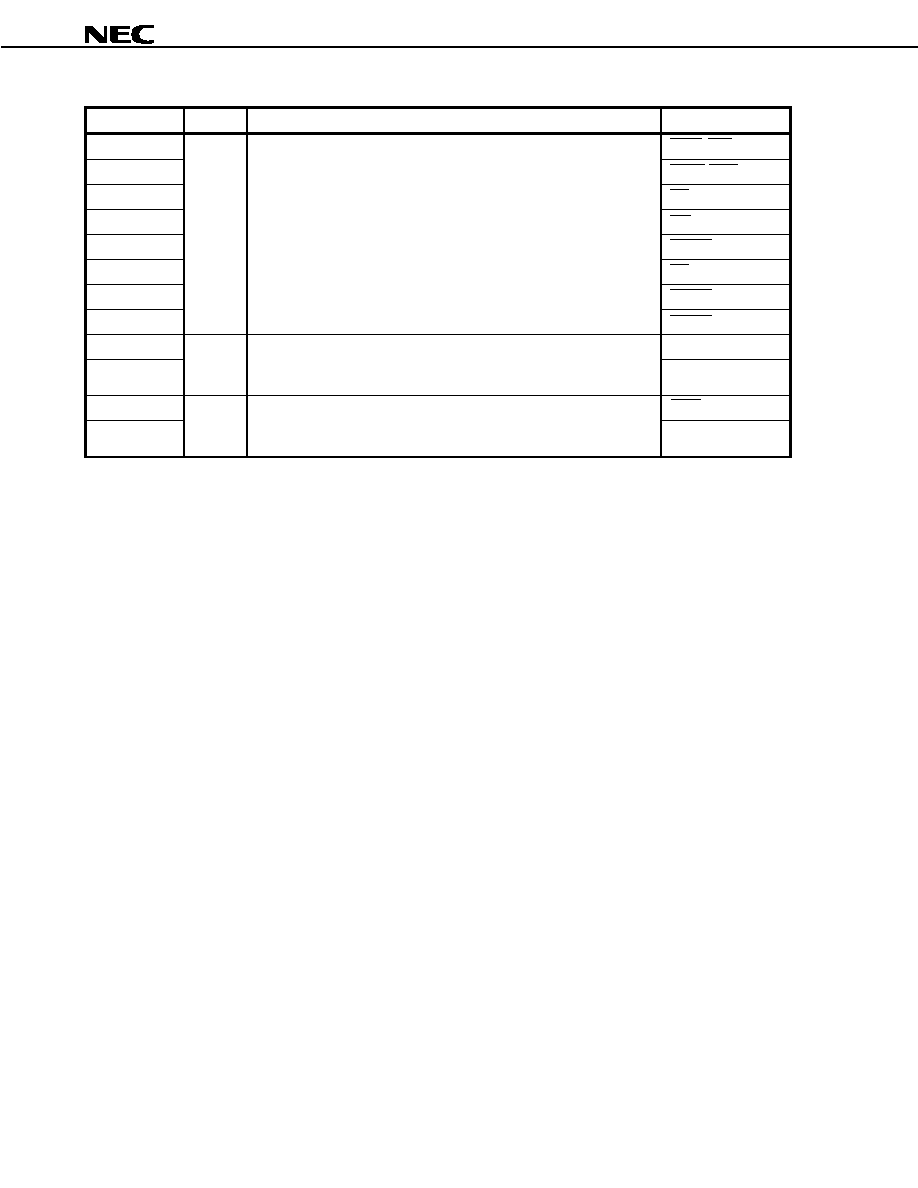
2.2 Non-Port Pins
(1/2)
Pin Name
I/O
Function
Alternate Function
TO100
P00
TO110
P10
TO120
Output
Pulse signal output for timers 10 to 12
P100
TCLR10
P02
TCLR11
P12
TCLR12
Input
External clear signal input for timers 10 to 12
P102
TI13
Input
External count clock input for timer 13
P33
INTP100
P04/DMARQ0
INTP101
P05/DMARQ1
INTP102
P06/DMARQ2
INTP103
Input
External maskable interrupt request input, shared as external capture
trigger input for timer 10
P07/DMARQ3
INTP110
P14/DMAAK0
INTP111
P15/DMAAK1
INTP112
P16/DMAAK2
INTP113
Input
External maskable interrupt request input, shared as external capture
trigger input for timer 11
P17/DMAAK3
INTP130
Input
External maskable interrupt request input, shared as external capture
trigger input for timer 13
P34
SO0
P22/TXD0
SO1
Output
Serial transmit data output (3-wire) for CSI0 and CSI1
P25/TXD1
SI0
P23/RXD0
SI1
Input
Serial receive data input (3-wire) for CSI0 and CSI1
P26/RXD1
SCK0
P24
SCK1
I/O
Serial clock I/O (3-wire) for CSI0 and CSI1
P27
TXD0
P22/SO0
TXD1
Output
Serial transmit data output for UART0 and UART1
P25/SO1
RXD0
P23/SI0
RXD1
Input
Serial receive data input for UART0 and UART1
P26/SI1
D0 to D7
≠
D8 to D15
I/O
16-bit data bus for external memory
P50 to P57
A0 to A15
≠
A16 to A23
Output
24-bit address bus for external memory
P60 to P67
LWR
Output
Lower byte write-enable signal output for external data bus
P90/LCAS
UWR
Output
Higher byte write-enable signal output for external data bus
P91/UCAS
RD
Output
Read strobe signal output for external data bus
P92
WE
Output
Write enable signal output for DRAM
P93
OE
Output
Output enable signal output for DRAM
P95
Preliminary Data Sheet U15390EJ1V0DS
10
µ
µ
µ
µ
PD703130
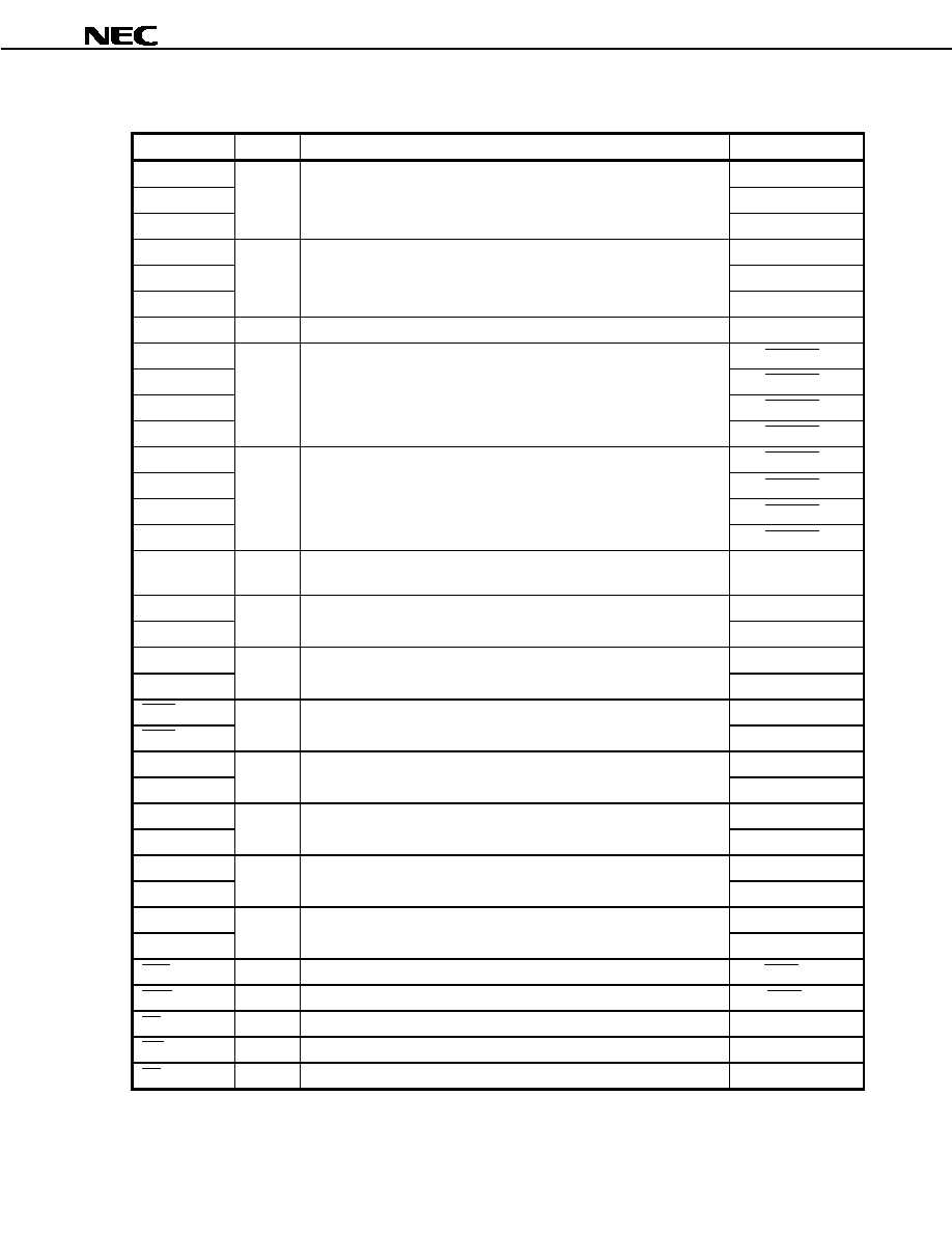
(2/2)
Pin Name
I/O
Function
Alternate Function
LCAS
Output
Column address strobe signal output for DRAM's lower data
P90/LWR
UCAS
Output
Column address strobe signal output for DRAM's higher data
P91/UWR
RAS3
P83/CS3
RAS4
P84/CS4/IOWR
RAS5
Output
Row address strobe signal output for DRAM
P85/CS5/IORD
BCYST
Output
Strobe signal output indicating start of bus cycle
P94
CS0
P80
CS3
P83/RAS3
CS4
P84/RAS4/IOWR
CS5
Output
Chip select signal output
P85/RAS5/IORD
WAIT
Input
Control signal input for inserting waits in bus cycle
PX6
IOWR
Output
DMA write strobe signal output
P84/RAS4/CS4
IORD
Output
DMA read strobe signal output
P85/RAS5/CS5
DMARQ0 to
DMARQ3
Input
DMA request signal input
P04/INTP100 to
P07/INTP103
DMAAK0 to
DMAAK3
Output
DMA acknowledge signal output
P14/INTP110 to
P17/INTP113
HLDAK
Output
Bus hold acknowledge output
P96
HLDRQ
Input
Bus hold request input
P97
ANI0 to ANI3
Input
Analog input to A/D converter
P70 to P73
NMI
Input
Non-maskable interrupt request input
P20
CLKOUT
Output
System clock output
PX7
CKSEL
Input
Input for specifying clock generator's operation mode
≠
MODE0,
MODE2
Input
Specify operation modes
≠
RESET
Input
System reset input
≠
X1
Input
≠
X2
≠
Connecting resonator for system clock. Input is via X1 when using an
external clock.
≠
AV
REF
Input
Reference voltage input for A/D converter
≠
AV
DD
≠
Positive power supply for A/D converter
≠
AV
SS
≠
Ground potential for A/D converter
≠
CV
DD
≠
Positive power supply for dedicated clock generator
≠
CV
SS
≠
Ground potential for dedicated clock generator
≠
V
DD
≠
Positive power supply (power supply for internal units)
≠
HV
DD
≠
Positive power supply (power supply for external pins)
≠
V
SS
≠
Ground potential
≠
Preliminary Data Sheet U15390EJ1V0DS
11
µ
µ
µ
µ
PD703130
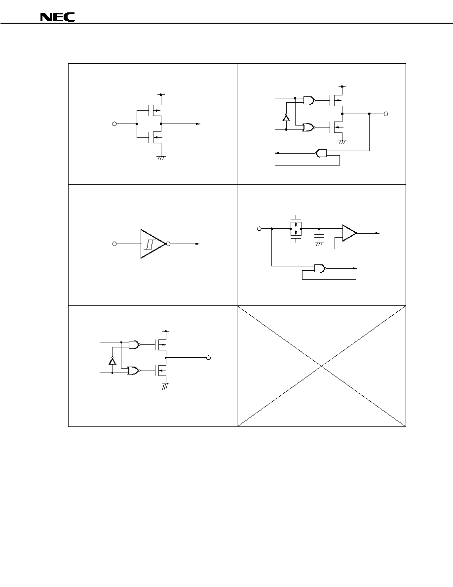
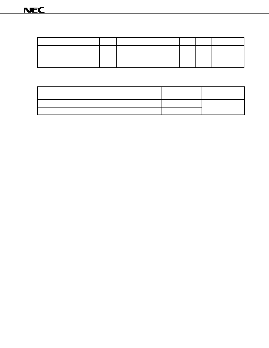
2.3 Pin I/O Circuits and Recommended Connection of Unused Pins
Table 2-1 shows the I/O circuit type of each pin and recommended connection of unused pins. Figure 2-1 shows
the various circuit types using partially abridged diagrams.
When connecting to V
DD
or V
SS
via a resistor, a resistance value in the range of 1 to 10 k
is recommended.
Table 2-1. I/O Circuit Type of Each Pin and Recommended Connection of Unused Pins (1/2)
Pin
I/O Circuit Type
Recommended Connection of Unused Pins
P00/TO100
P02/TCLR10
P04/INTP100/DMARQ0 to
P07/INTP103/DMARQ3
P10/TO110
P12/TCLR11
P14/INTP110/DMAAK0 to
P17/INTP113/DMAAK3
5
Input: Independently connect to HV
DD
or V
SS
via a resistor
Output: Leave open
P20/NMI
2
Connect directly to V
SS
P22/TXD0/SO0
P23/RXD0/SI0
P24/SCK0
P25/TXD1/SO1
P26/RXD1/SI1
P27/SCK1
P33/TI13
P34/INTP130
P50/D8 to P57/D15
P60/A16 to P67/A23
5
Input: Independently connect to HV
DD
or V
SS
via a resistor
Output: Leave open
P70/ANI0 to P73/ANI3
9
Connect directly to V
SS
P80/CS0, to P83/CS3/RAS3
P84/CS4/RAS4/IOWR,
P85/CS5/RAS5/IORD
P90/LCAS/LWR
P91/UCAS/UWR
P92/RD
P93/WE
P94/BCYST
P95/OE
P96/HLDAK
P97/HLDRQ
P100/TO120
P102/TCLR12
5
Input: Independently connect to HV
DD
or V
SS
via a resistor
Output: Leave open
Preliminary Data Sheet U15390EJ1V0DS
12
µ
µ
µ
µ
PD703130
Table 2-1. I/O Circuit Type of Each Pin and Recommended Connection of Unused Pins (2/2)
Pin
I/O Circuit Type
Recommended Connection of Unused Pins
PX6/WAIT
PX7/CLKOUT
5
Input: Independently connect to HV
DD
or V
SS
via a resistor
Output: Leave open
A0 to A15
4
D0 to D7
5
CKSEL
1
RESET
MODE0, MODE2
2
≠
AV
REF
, AV
SS
≠
Connect directly to V
SS
AV
DD
≠
Connect directly to HV
DD
Preliminary Data Sheet U15390EJ1V0DS
13
µ
µ
µ
µ
PD703130
Figure 2-1. Pin I/O Circuits
IN
P-ch
V
DD
N-ch
IN
Data
P-ch
V
DD
N-ch
IN/OUT
Output
disable
Input
enable
IN
+
≠
Input enable
P-ch
N-ch
V
REF
(threshold voltage)
Type 1
Type 2
Type 5
Type 9
Comparator
Schmitt-triggered input with hysteresis characteristics
Type 4
P-ch
N-ch
V
DD
OUT
Data
Output
disable
Push-pull output with possible high-impedance output
(P-ch, N-ch both off)
Caution Replace V
DD
by HV
DD
when referencing the circuit diagrams shown above.
Preliminary Data Sheet U15390EJ1V0DS
14
µ
µ
µ
µ
PD703130
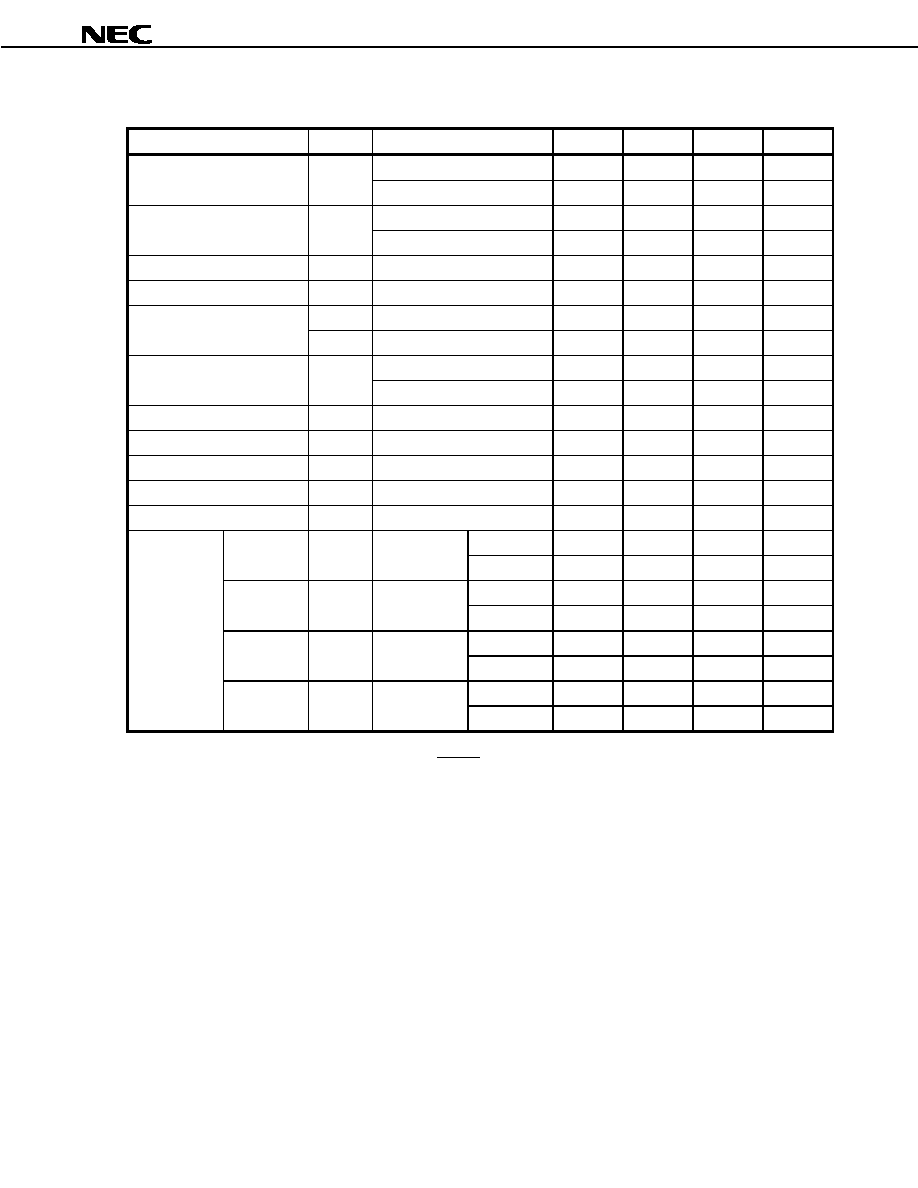
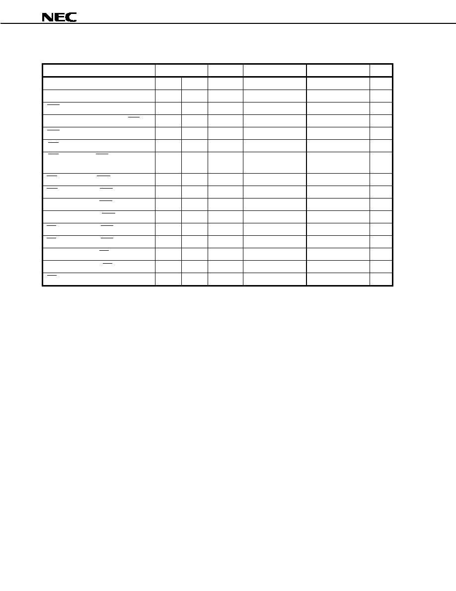
3. ELECTRICAL SPECIFICATIONS
Absolute Maximum Ratings (T
A
= 25
∞
∞
∞
∞C)
Parameter
Symbol
Condition
Rating
Unit
V
DD
V
DD
pin
-0.5 to +4.6
V
HV
DD
HV
DD
pin, HV
DD
V
DD
-0.5 to +7.0
V
CV
DD
CV
DD
pin
-0.5 to +4.6
V
CV
SS
CV
SS
pin
-0.5 to +0.5
V
AV
DD
AV
DD
pin
-0.5 to HV
DD
+ 0.5
Note
V
Power supply voltage
AV
SS
AV
SS
pin
-0.5 to +0.5
V
Input voltage
V
I
Except X1 pin
-0.5 to HV
DD
+ 0.5
Note
V
Clock input voltage
V
K
X1, V
DD
= 3.0 to 3.6 V
-0.5 to V
DD
+ 1.0
Note
V
1 pin
4.0
mA
Output current, low
I
OL
Total of all pins
100
mA
1 pin
-4.0
mA
Output current, high
I
OH
Total of all pins
-100
mA
Output voltage
V
O
HV
DD
= 5.0 V
±10%
-0.5 to HV
DD
+ 0.5
Note
V
AV
DD
> HV
DD
-0.5 to HV
DD
+ 0.5
Note
V
Analog input voltage
V
IAN
P70/ANI0 to P73
pins
HV
DD
AV
DD
-0.5 to AV
DD
+ 0.5
Note
V
AV
DD
> HV
DD
-0.5 to HV
DD
+ 0.5
Note
V
A/D converter reference input
voltage
AV
REF
HV
DD
AV
DD
-0.5 to AV
DD
+ 0.5
Note
V
Operating ambient temperature
T
A
-40 to +85
∞C
Storage temperature
T
stg
-60 to +150
∞C
Note Be sure not to exceed the absolute maximum ratings (MAX. value) of the each power supply voltage.
Cautions 1. Do not make direct connections of the output (or input/output) pins of the IC product with
each other, and also avoid direct connections to V
DD
, V
CC
, or GND. However, the open drain
pins or the open collector pins can be directly connected to each other. A direct connection
can also be made for an external circuit designed with timing specifications that prevent
conflicting output from pins subject to a high-impedance state.
2. Product quality may suffer if the absolute maximum rating is exceeded even momentarily for
any parameter. That is, the absolute maximum ratings are rated values at which the product
is on the verge of suffering physical damage, and therefore the product must be used under
conditions that ensure that the absolute maximum ratings are not exceeded.
The ratings and conditions shown below for DC characteristics and AC characteristics are
within the range for normal operation and quality assurance.
Preliminary Data Sheet U15390EJ1V0DS
15
µ
µ
µ
µ
PD703130
Capacitance (T
A
= 25
∞
∞
∞
∞C, V
DD
= HV
DD
= CV
DD
= V
SS
= 0 V)
Parameter
Symbol
Condition
MIN.
TYP.
MAX.
Unit
Input capacitance
C
I
15
pF
I/O capacitance
C
IO
15
pF
Output capacitance
C
O
f
c
= 1 MHz
Unmeasured pins returned to 0 V.
15
pF
Operating Conditions
Operation Mode
Internal Operating Clock Frequency (f
X
)
Operating Ambient
Temperature (T
A
)
Power Supply Voltage
(V
DD
, HV
DD
)
Direct mode
10 to 33 MHz
Note 1
-40 to +85∞C
PLL mode
Note 2
20 to 33 MHz
Note 3
-40 to +85∞C
V
DD
= 3.0 to 3.6 V,
HV
DD
= 5.0 V
±10%
Notes 1. Set the input clock frequency used in direct mode to 20 to 66 MHz.
2. The internal operating clock frequency in PLL mode is the value for 5
◊ operation. When used for 1◊ or
1/2
◊ operation as set by the CKDIVn (n = 0, 1) bit of the CKC register, operation at a frequency of 20
MHz or less is possible.
3. Set the input clock frequency used in PLL mode to 4.0 to 6.6 MHz.
Preliminary Data Sheet U15390EJ1V0DS
16
µ
µ
µ
µ
PD703130
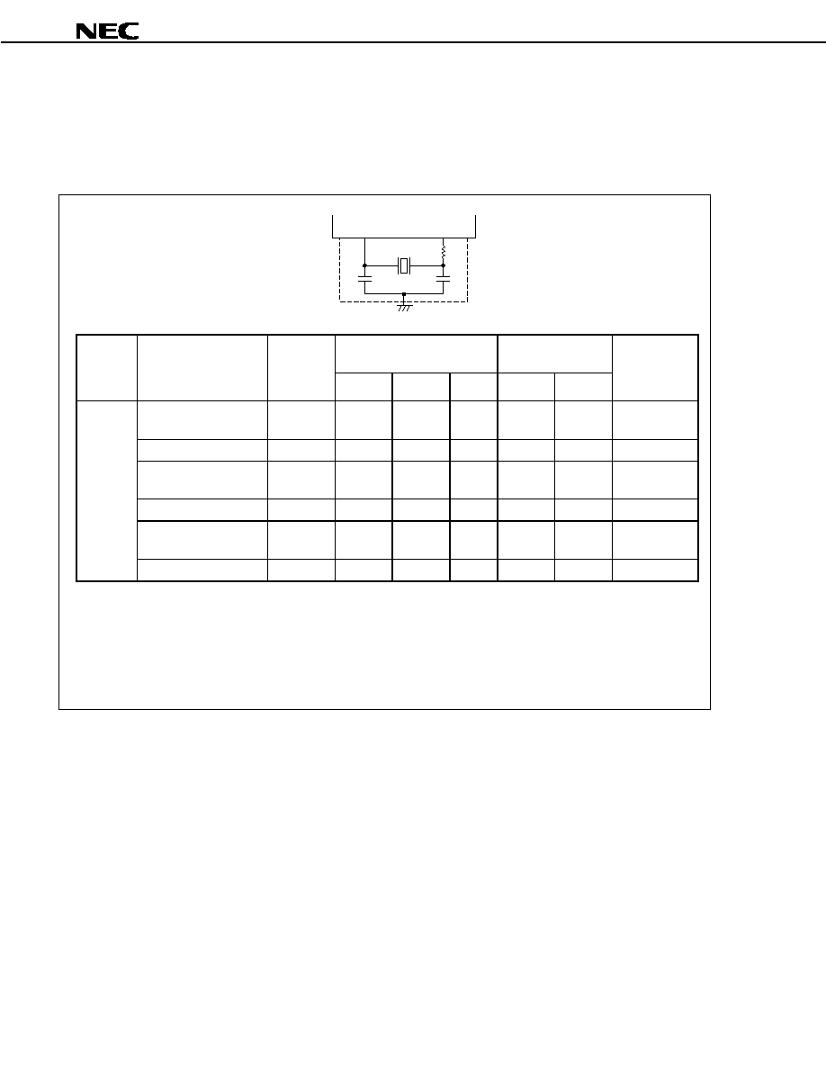
Recommended Oscillator
(a) Ceramic resonator
(i) Murata Mfg. Co., Ltd. (T
A
=
-
-
-
-40 to +85∞∞∞∞C)
Recommended Circuit Constant
Oscillation Voltage
Range
Manu-
facturer
Part Number
Oscillation
Frequency
f
XX
(MHz)
C1 (pF)
C2 (pF)
R
d
(k
) MIN. (V)
MAX. (V)
Oscillation
Stabilization
Time (MAX.)
T
OST
(ms)
CSTS400MG06
Note
(CSTLS4M00G56-B0)
4.0
On-chip
On-chip
0
3.0
3.6
0.6
CSTCR4M00G55-R0
4.0
On-chip
On-chip
0
3.0
3.6
0.6
CSTS0500MG06
Note
(CSTLS5M00G56-B0)
5.0
On-chip
On-chip
0
3.0
3.6
0.6
CSTCR5M00G55-R0
5.0
On-chip
On-chip
0
3.0
3.6
0.6
CSTS066MG06
Note
(CSTLS6M60G56-B0)
6.6
On-chip
On-chip
0
3.0
3.6
0.6
Murata
Mfg.
CSTCR6M60G55-R0
6.6
On-chip
On-chip
0
3.0
3.6
0.6
Note The part number will be changed to the part number in the parentheses from June 2001.
Cautions 1. Connect the oscillator as close to the X1 and X2 pins as possible.
2. Do not wire any other signal lines in the area enclosed by broken lines.
3. Sufficiently evaluate the matching between the
µ
µ
µ
µPD703130 and the resonator.
X1
C1
X2
C2
R
d
Preliminary Data Sheet U15390EJ1V0DS
17
µ
µ
µ
µ
PD703130
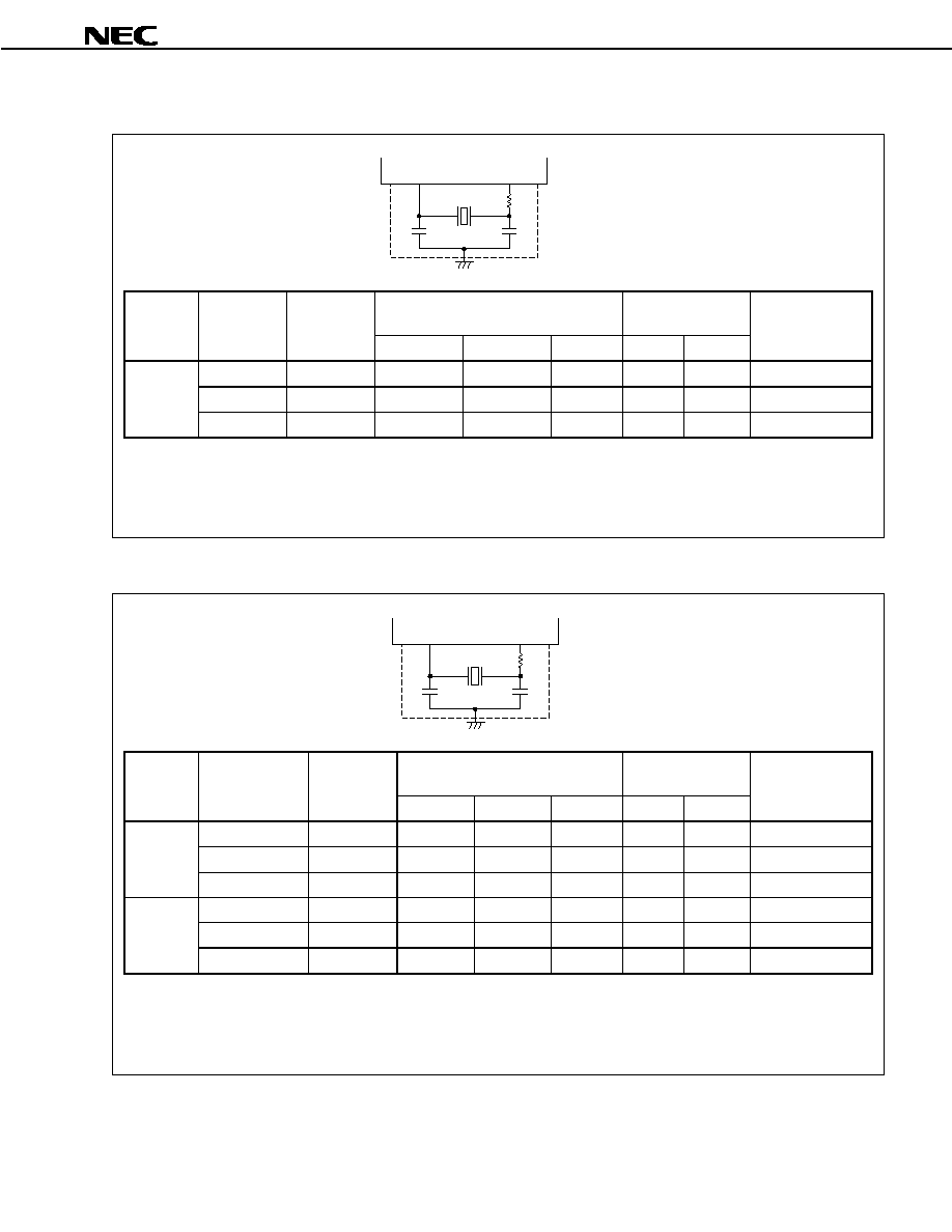
(ii) TDK (T
A
=
-
-
-
-40 to +85∞∞∞∞C)
Recommended Circuit Constant
Oscillation
Voltage Range
Manu-
facturer
Part Number
Oscillation
Frequency
f
XX
(MHz)
C1 (pF)
C2 (pF)
R
d
(k
)
MIN. (V) MAX. (V)
Oscillation
Stabilization Time
(MAX.) T
OST
(ms)
FCR4.0MC5
4.0
On-chip
On-chip
0
3.0
3.6
0.73
FCR5.0MC5
5.0
On-chip
On-chip
0
3.0
3.6
0.68
TDK
FCR6.0MC5
6.0
On-chip
On-chip
0
3.0
3.6
0.58
Cautions 1. Connect the oscillator as closely to the X1 and X2 pins as possible.
2. Do not wire any other signal lines in the area enclosed by broken lines.
3. Sufficiently evaluate the matching between the
µ
µ
µ
µPD703130 and the resonator.
(iii) Kyocera Corporation (T
A
=
-
-
-
-20 to +80∞∞∞∞C)
Recommended Circuit Constant
Oscillation
Voltage Range
Type
Part Number
Oscillation
Frequency
f
XX
(MHz)
C1 (pF)
C2 (pF)
R
d
(k
)
MIN. (V)
MAX. (V)
Oscillation
Stabilization Time
(MAX.) T
OST
(ms)
KBR-4.0MKC
4.0
On-chip
On-chip
0
3.0
3.6
0.80
KBR-5.0MKC
5.0
On-chip
On-chip
0
3.0
3.6
0.70
Lead
KBR-6.0MKC
6.0
On-chip
On-chip
0
3.0
3.6
0.76
PBRC4.00HR
4.0
On-chip
On-chip
0
3.0
3.6
0.80
PBRC5.00HR
5.0
On-chip
On-chip
0
3.0
3.6
0.70
SMD
PBRC6.00HR
6.0
On-chip
On-chip
0
3.0
3.6
0.76
Cautions 1. Connect the oscillator as close to the X1 and X2 pins as possible.
2. Do not wire any other signal lines in the area enclosed by broken lines.
3. Sufficiently evaluate the matching between the
µ
µ
µ
µPD703130 and the resonator.
X1
C1
X2
C2
R
d
X1
C1
X2
C2
R
d
Preliminary Data Sheet U15390EJ1V0DS
18
µ
µ
µ
µ
PD703130
(b) External clock input (T
A
= ≠40 to +85
∞
∞
∞
∞C)
X1
X2
Open
External clock
Caution Input CMOS-level voltage to the X1 pin.
Preliminary Data Sheet U15390EJ1V0DS
19
µ
µ
µ
µ
PD703130
DC Characteristics (T
A
= ≠40 to +85
∞
∞
∞
∞C, V
DD
= CV
DD
= 3.0 to 3.6 V, HV
DD
= 5.0
±
±
±
±10%, V
SS
= 0 V)
Parameter
Symbol
Condition
MIN.
TYP.
MAX.
Unit
Except Note 1
2.2
HV
DD
+ 0.3
V
Input voltage, high
V
IH
Note 1
0.8HV
DD
HV
DD
+ 0.3
V
Except Note 1 and Note 2
-0.5
+0.8
V
Input voltage, low
V
IL
Note 1
-0.5
0.2HV
DD
V
Clock input voltage, high
V
XH
X1 pin
0.8V
DD
V
DD
+ 0.3
V
Clock input voltage, low
V
XL
X1 pin
-0.3
0.15V
DD
V
HV
T
+
Note 1, rising edge
3.0
V
Schmitt-triggered input
threshold voltage
HV
T
-
Note 1, falling edge
2.0
V
I
OH
=
-2.5 mA
0.7HV
DD
V
Output voltage, high
V
OH
I
OH
=
-100
µA
HV
DD
- 0.4
V
Output voltage, low
V
OL
I
OL
= 2.5 mA
0.45
V
Input leakage current, high
I
LIH
V
I
= HV
DD
, except Note 2
10
µA
Input leakage current, low
I
LIL
V
I
= 0 V, except Note 2
-10
µA
Output leakage current, high
I
LOH
V
O
= HV
DD
10
µA
Output leakage current, low
I
LOL
V
O
= 0 V
-10
µA
V
DD
+ CV
DD
2.0
◊ fx
3.0
◊ fx
mA
Normal
mode
I
DD1
HV
DD
1.5
◊ fx
2.5
◊ fx
mA
V
DD
+ CV
DD
1.4
◊ fx
1.8
◊ fx
mA
HALT mode
I
DD2
HV
DD
0.7
◊ fx
1.2
◊ fx
mA
V
DD
+ CV
DD
1.4
2.5
mA
IDLE mode
I
DD3
HV
DD
20
100
µA
V
DD
+ CV
DD
20
100
µA
Power supply
current
STOP
mode
I
DD4
HV
DD
10
50
µA
Notes 1. P20/NMI, MODE0, MODE2, CKSEL, RESET
2. When the P70/ANI0 to P73/ANI3 pins are used as analog input.
Remarks 1. TYP. values are reference values for when T
A
= 25∞C, V
DD
= CV
DD
= 3.3 V, and HV
DD
= 5.0 V.
2. Direct mode: f
X
= 10 to 33 MHz
PLL mode: f
X
= 20 to 33 MHz
3. The unit for f
X
is MHz.
Preliminary Data Sheet U15390EJ1V0DS
20
µ
µ
µ
µ
PD703130
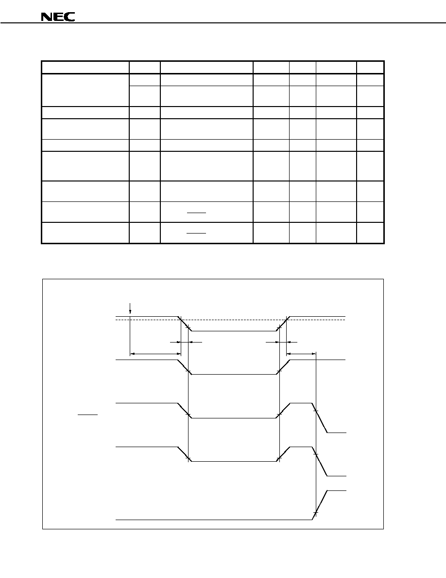
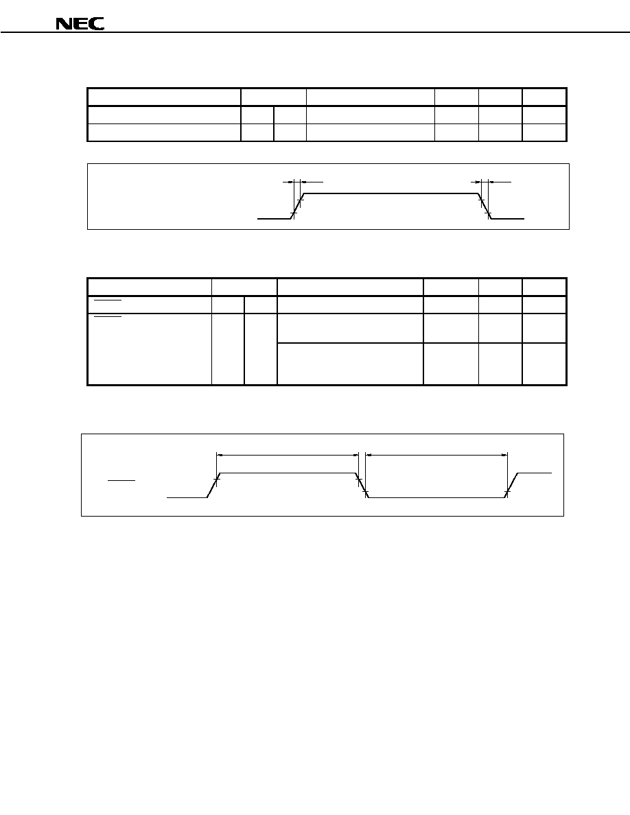
Data Hold Characteristics (T
A
= ≠40 to +85
∞
∞
∞
∞C)
Parameter
Symbol
Condition
MIN.
TYP.
MAX.
Unit
V
DDDR
STOP mode, V
DD
= V
DDDR
1.5
3.6
V
Data hold voltage
HV
DDDR
STOP mode,
HV
DD
= HV
DDDR
V
DDDR
5.5
V
Data hold current
I
DDDR
V
DD
= V
DDDR
30
150
µA
Power supply voltage rise
time
t
RVD
200
µs
Power supply voltage fall time
t
FVD
200
µs
Power supply voltage hold
time (from STOP mode
setting)
t
HVD
0
ms
STOP mode release signal
input time
t
DREL
0
ns
Data hold input voltage, high
V
IHDR
P20/NMI, MODE0, MODE2,
CKSEL, RESET
0.8HV
DDDR
HV
DDDR
V
Data hold input voltage, low
V
ILDR
P20/NMI, MODE0, MODE2,
CKSEL, RESET
0
0.2HV
DDDR
V
Remark TYP. values are reference values for when T
A
= 25
∞C.
HV
DD
RESET (Input)
V
IHDR
V
IHDR
V
ILDR
V
DD
t
HVD
t
FVD
V
DDDR
t
RVD
t
DREL
STOP mode setting
NMI (Input)
(Released by falling edge)
NMI (Input)
(Released by rising edge)
3.0 V
Preliminary Data Sheet U15390EJ1V0DS
21
µ
µ
µ
µ
PD703130
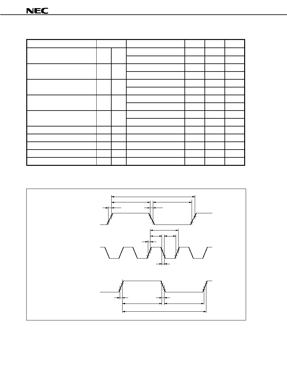
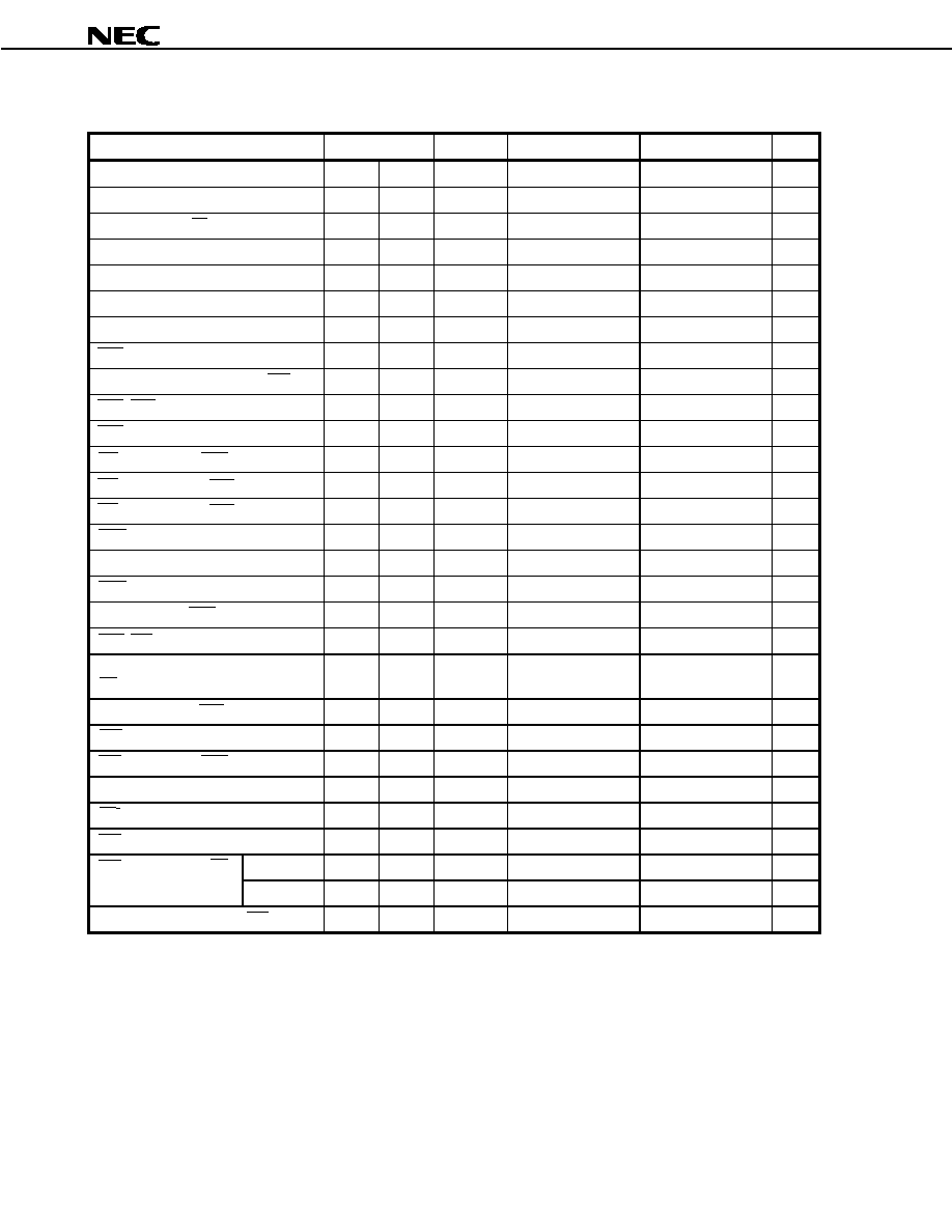
AC Characteristics (T
A
= ≠40 to +85
∞
∞
∞
∞C, V
DD
= CV
DD
= 3.0 to 3.6 V, HV
DD
= 5.0
±
±
±
±10%, V
SS
= 0 V, output pin load
capacitance: C
L
= 50 pF)
AC Test Input Test Points
(a) P20/NMI, MODE0, MODE2, CKSEL, RESET
HV
DD
0 V
0.8HV
DD
0.2HV
DD
0.8HV
DD
0.2HV
DD
Test
points
Input signal
(b) Pins other than those listed in (a) above
2.4 V
0.4 V
2.2 V
0.8 V
2.2 V
0.8 V
Test
points
Input signal
AC Test Output Test Points
Load Condition
Caution In cases where the load capacitance is greater than 50 pF due to the circuit configuration,
insert a buffer or other element to reduce the device's load capacitance 50 pF.
2.4 V
0.8 V
2.4 V
0.8 V
Test
points
Output signal
C
L
= 50 pF
DUT
(Device under test)
Preliminary Data Sheet U15390EJ1V0DS
22
µ
µ
µ
µ
PD703130
(1) Clock timing
Parameter
Symbol
Condition
MIN.
MAX.
Unit
Direct mode
15
50
ns
X1 input cycle
<1>
t
CYX
PLL mode
150
250
ns
Direct mode
5
ns
X1 input high-level width
<2>
t
WXH
PLL mode
50
ns
Direct mode
5
ns
X1 input low-level width
<3>
t
WXL
PLL mode
50
ns
Direct mode
4
ns
X1 input rise time
<4>
t
XR
PLL mode
10
ns
X1 input fall time
<5>
t
XF
Direct mode
4
ns
PLL mode
10
ns
CLKOUT output cycle
<6>
t
CYK
30
100
ns
CLKOUT high-level width
<7>
t
WKH
0.5T ≠ 7
ns
CLKOUT low-level width
<8>
t
WKL
0.5T ≠ 4
ns
CLKOUT rise time
<9>
t
KR
5
ns
CLKOUT fall time
<10>
t
KF
5
ns
Remark T = t
CYK
<4>
<5>
<2>
<3>
<1>
X1
(PLL mode)
<1>
<2>
<3>
<4>
<5>
<9>
<10>
<7>
<8>
<6>
X1
(Direct mode)
CLKOUT (Output)
Preliminary Data Sheet U15390EJ1V0DS
23
µ
µ
µ
µ
PD703130
(2) Output waveform (other than X1, CLKOUT)
Parameter
Symbol
Condition
MIN.
MAX.
Unit
Output rise time
<12>
t
OR
10
ns
Output fall time
<13>
t
OF
10
ns
<13>
Signals other than X1, CLKOUT
<12>
(3) Reset timing
Parameter
Symbol
Condition
MIN.
MAX.
Unit
RESET high-level width
<14>
t
WRSH
500
ns
When power supply is on, and
STOP mode has been released
500 + T
OS
ns
RESET low-level width
<15>
t
WRSL
Other than when power supply is
on, and STOP mode has been
released
500
ns
Remark T
OS
: Oscillation stabilization time
<14>
<15>
RESET (Input)
Preliminary Data Sheet U15390EJ1V0DS
24
µ
µ
µ
µ
PD703130
(4) SRAM, external ROM, or external I/O access timing
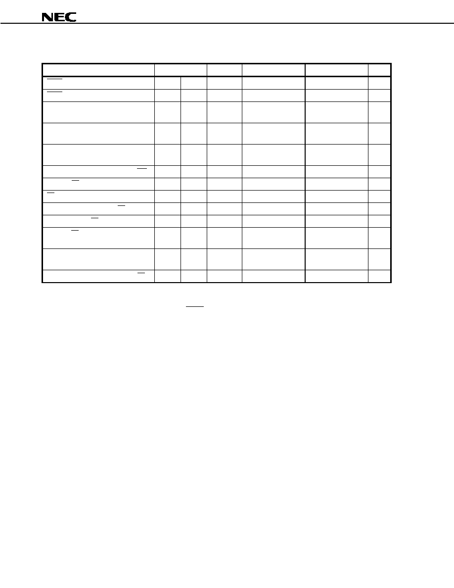
(a) Access timing (SRAM, external ROM, or external I/O) (1/2)
Parameter
Symbol
Condition
MIN.
MAX.
Unit
Address, CSn output delay time (from
CLKOUT
)
<16>
t
DKA
2
10
ns
Address, CSn output hold time (from
CLKOUT
)
<17>
t
HKA
2
10
ns
RD, IORD
delay time
(from CLKOUT
)
<18>
t
DKRDL
2
14
ns
RD, IORD
delay time
(from CLKOUT
)
<19>
t
HKRDH
2
14
ns
UWR, LWR, IOWR
delay time (from
CLKOUT
)
<20>
t
DKWRL
2
10
ns
UWR, LWR, IOWR
delay time (from
CLKOUT
)
<21>
t
HKWRH
2
10
ns
BCYST
delay time (from CLKOUT
)
<22>
t
DKBSL
2
10
ns
BCYST
delay time (from CLKOUT
)
<23>
t
HKBSH
2
10
ns
WAIT setup time (to CLKOUT
)
<24>
t
SWK
15
ns
WAIT hold time (from CLKOUT
)
<25>
t
HKW
2
ns
Data input setup time
(to CLKOUT
)
<26>
t
SKID
18
ns
Data input hold time
(from CLKOUT
)
<27>
t
HKID
2
ns
Data output delay time
(from CLKOUT
)
<28>
t
DKOD
2
10
ns
Data output hold time
(from CLKOUT
)
<29>
t
HKOD
2
10
ns
Remarks 1. Maintain at least one of the data input hold times t
HKID
and t
HRDID
.
2. n = 0, 3 to 5
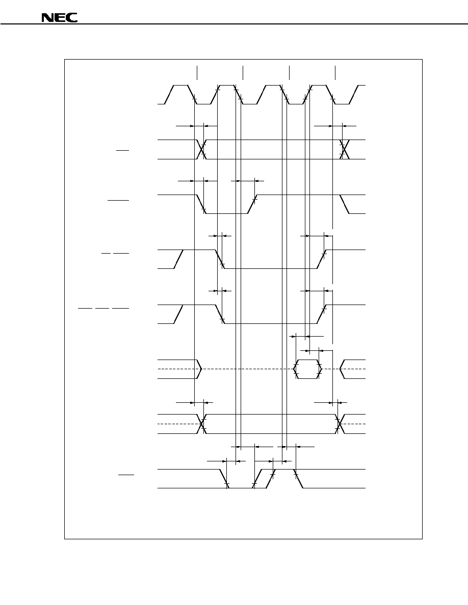
Preliminary Data Sheet U15390EJ1V0DS
25
µ
µ
µ
µ
PD703130
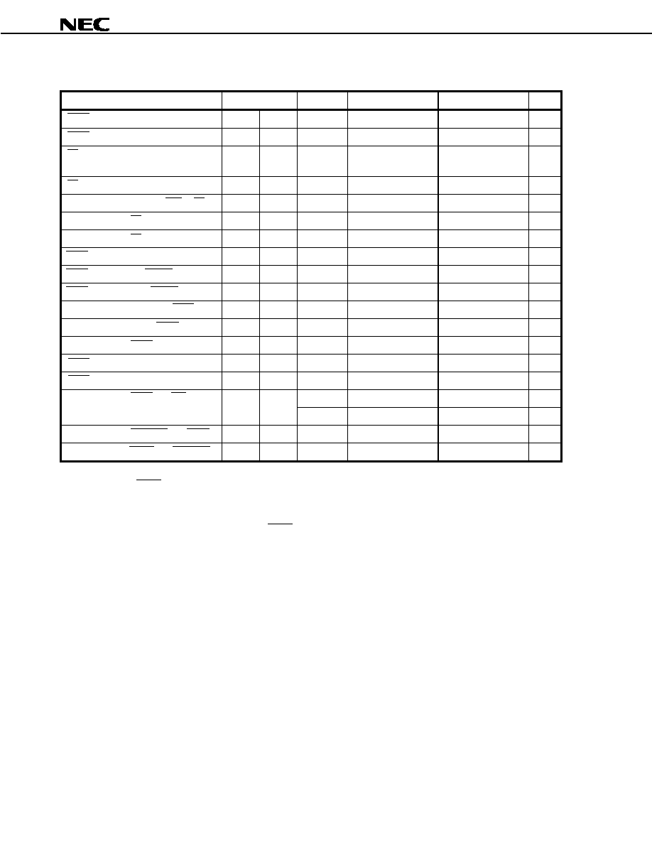
(a) Access timing (SRAM, external ROM, or external I/O) (2/2)
Remarks 1. This is the timing when the number of waits due to the DWC1 and DWC2 registers is zero.
2. The broken lines indicate high impedance.
3. n = 0, 3 to 5
CLKOUT (Output)
A0 to A23 (Output)
CSn (Output)
BCYST (Output)
RD, IORD (Output)
[Read time]
UWR, LWR, IOWR (Output)
[Write time]
D0 to D15 (I/O)
[Read time]
D0 to D15 (I/O)
[Write time]
WAIT (Input)
<16>
<17>
<22>
<23>
<18>
<19>
<20>
<21>
<26>
<27>
<28>
<29>
<24>
<25>
<24>
<25>
T1
TW
T2
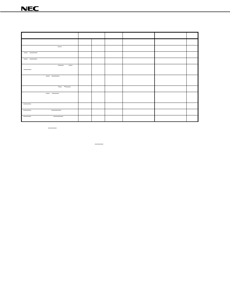
Preliminary Data Sheet U15390EJ1V0DS
26
µ
µ
µ
µ
PD703130
(b) Read timing (SRAM, external ROM, or external I/O) (1/2)
Parameter
Symbol
Condition
MIN.
MAX.
Unit
Data input setup time (to address)
<30>
t
SAID
(1.5 + w
D
+ w)T ≠ 28
ns
Data input setup time (to RD)
<31>
t
SRDID
(1 + w
D
+ w)T ≠ 32
ns
RD, IORD low-level width
<32>
t
WRDL
(1 + w
D
+ w)T ≠ 10
ns
RD, IORD high-level width
<33>
t
WRDH
T ≠ 10
ns
Delay time from address, CSn to RD,
IORD
<34>
t
DARD
0.5T ≠ 10
ns
Delay time from RD, IORD
to
address
<35>
t
DRDA
(0.5 + i)T ≠ 10
ns
Data input hold time (from RD, IORD
)
<36>
t
HRDID
0
ns
Delay time from RD, IORD
to data
output
<37>
t
DRDOD
(0.5 + i)T ≠ 10
ns
WAIT setup time (to address)
<38>
t
SAW
Note
T ≠ 25
ns
WAIT setup time (to BCYST
)
<39>
t
SBSW
Note
T ≠ 25
ns
WAIT hold time (from BCYST
)
<40>
t
HBSW
Note
0
ns
Note For first WAIT sampling when the number of waits due to the DWC1 and DWC2 registers is zero.
Remarks 1. T = t
CYK
2. w: The number of waits due to WAIT.
3. w
D
: The number of waits due to the DWC1 and DWC2 registers.
4. i: The number of idle states that are inserted when a write cycle follows a read cycle.
5. Maintain at least one of the data input hold times, t
HKID
or t
HRDID
.
6. n = 0, 3 to 5
Preliminary Data Sheet U15390EJ1V0DS
27
µ
µ
µ
µ
PD703130
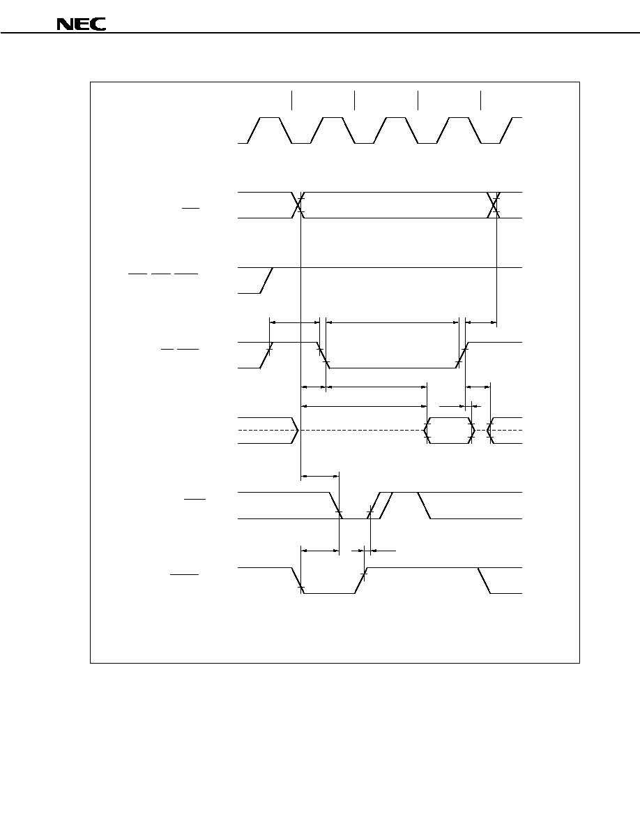
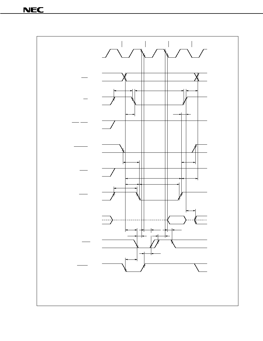
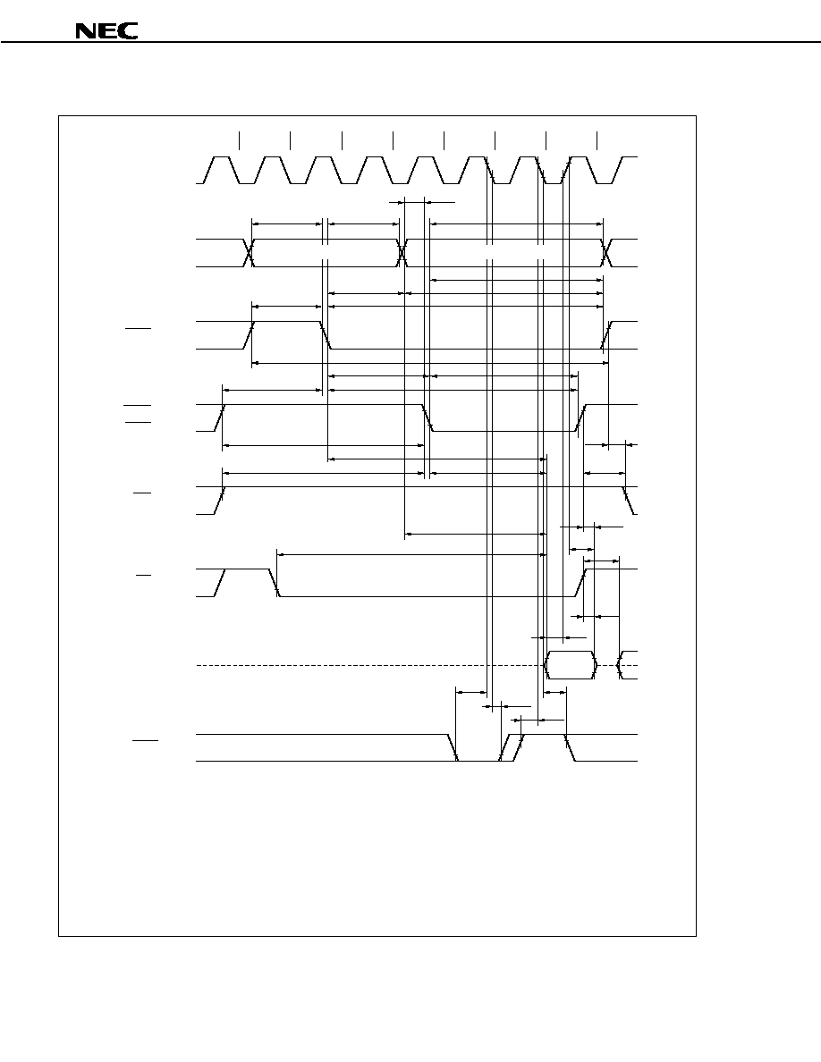
(b) Read timing (SRAM, external ROM, or external I/O) (2/2)
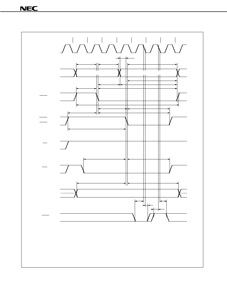
Remarks 1. This is the timing when the number of waits due to the DWC1 and DWC2 registers is zero.
2. The broken lines indicate high impedance.
3. n = 0, 3 to 5
UWR, LWR, IOWR (Output)
RD, IORD (Output)
D0 to D15 (I/O)
T1
TW
T2
CLKOUT (Output)
<33>
<32>
<35>
<38>
<34>
<31>
<30>
<36>
<37>
<39>
<40>
A0 to A23 (Output)
CSn (Output)
WAIT (Input)
BCYST (Output)
Preliminary Data Sheet U15390EJ1V0DS
28
µ
µ
µ
µ
PD703130
(c) Write timing (SRAM, external ROM, or external I/O) (1/2)
Parameter
Symbol
Condition
MIN.
MAX.
Unit
WAIT setup time (to address)
<38>
t
SAW
Note
T ≠ 25
ns
WAIT setup time (to BCYST
)
<39>
t
SBSW
Note
T ≠ 25
ns
WAIT hold time (from BCYST
)
<40>
t
HBSW
Note
0
ns
Delay time from address, CSn to
UWR, LWR, IOWR
<41>
t
DAWR
0.5T ≠ 10
ns
Address setup time (to UWR, LWR,
IOWR
)
<42>
t
SAWR
(1.5 + w
D
+ w)T ≠ 10
ns
Delay time from UWR, LWR, IOWR
to address
<43>
t
DWRA
0.5T ≠ 10
ns
UWR, LWR, IOWR high-level width
<44>
t
WWRH
T ≠ 10
ns
UWR, LWR, IOWR low-level width
<45>
t
WWRL
(1 + w
D
+ w)T ≠ 10
ns
Data output setup time
(to UWR, LWR, IOWR
)
<46>
t
SODWR
(1.5 + w
D
+ w)T ≠ 10
ns
Data output hold time
(from UWR, LWR, IOWR
)
<47>
t
HWROD
0.5T ≠ 10
ns
Note For first WAIT sampling when the number of waits due to the DWC1 and DWC2 registers is zero.
Remarks 1. T = t
CYK
2. w: The number of waits due to WAIT.
3. w
D
: The number of waits due to the DWC1 and DWC2 registers.
4. n = 0, 3 to 5
Preliminary Data Sheet U15390EJ1V0DS
29
µ
µ
µ
µ
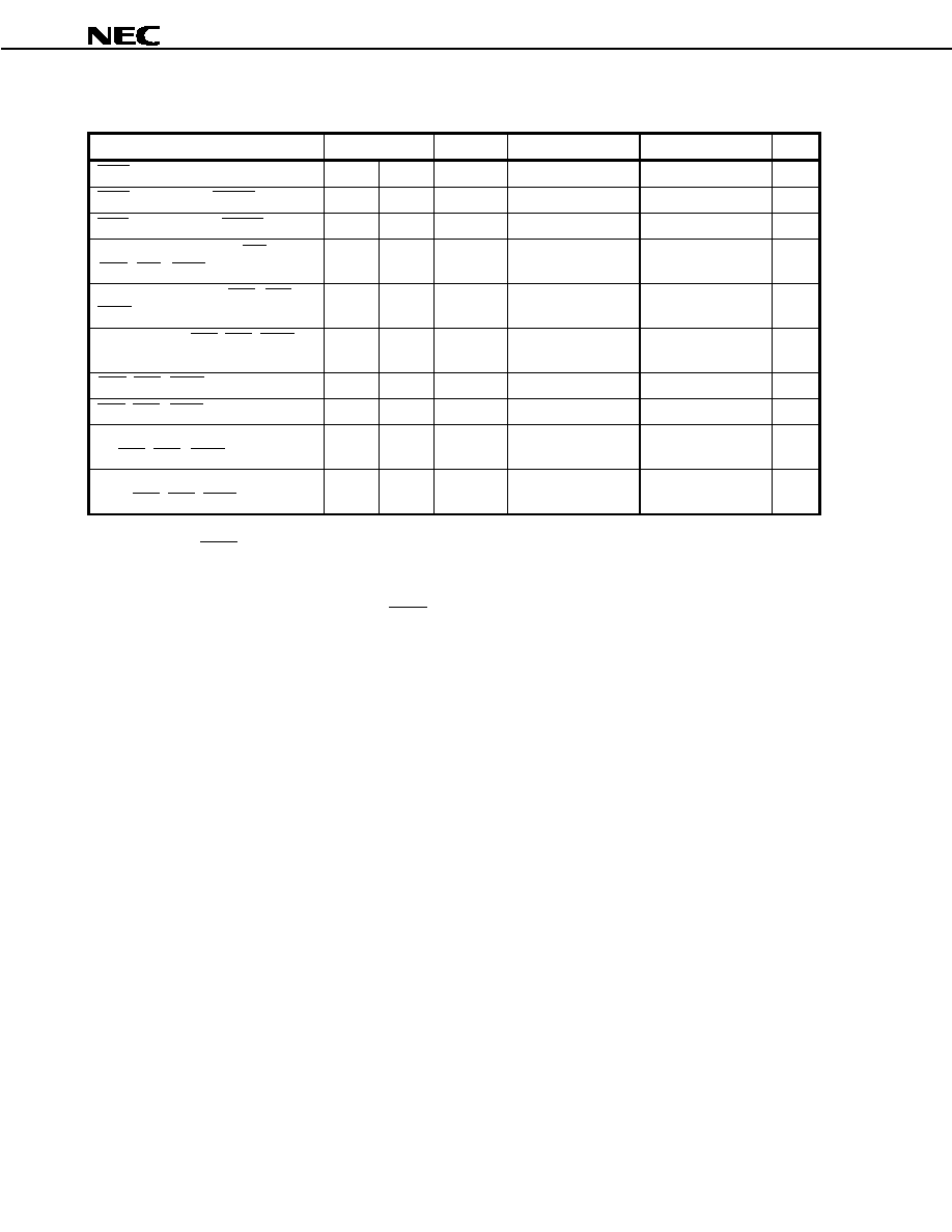
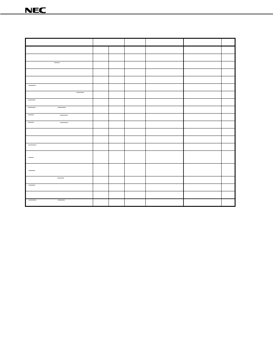
PD703130
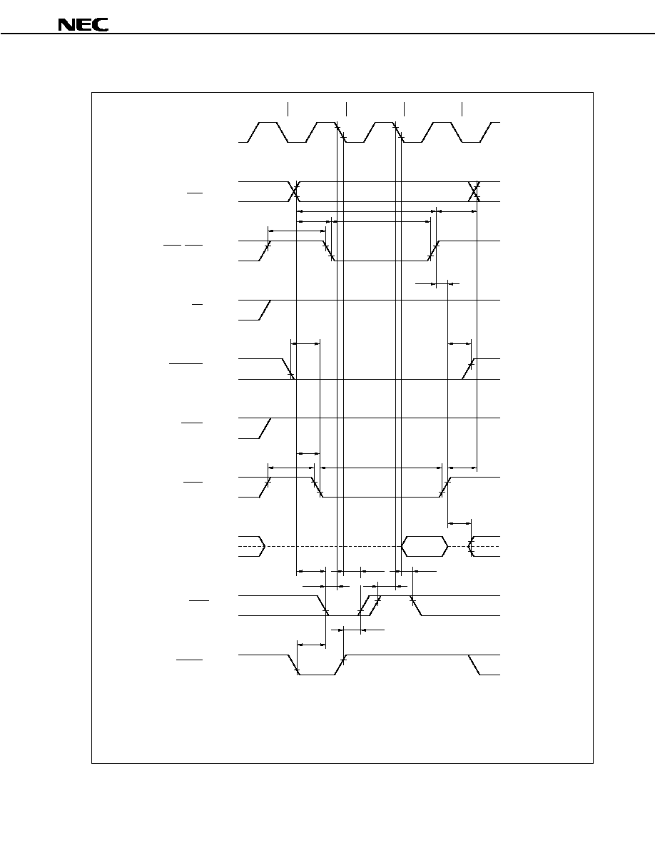
(c) Write timing (SRAM, external ROM, or external I/O) (2/2)
Remarks 1. This is the timing when the number of waits due to the DWC1 and DWC2 registers is zero.
2. The broken lines indicate high impedance.
3. n = 0, 3 to 5
T1
TW
T2
CLKOUT (Output)
<44>
<45>
<43>
<38>
<46>
<47>
<39>
<40>
<41>
<42>
A0 to A23 (Output)
CSn (Output)
RD, IORD (Output)
UWR, LWR, IOWR (Output)
D0 to D15 (I/O)
WAIT (Input)
BCYST (Output)
Preliminary Data Sheet U15390EJ1V0DS
30
µ
µ
µ
µ
PD703130
(d) DMA flyby transfer timing (SRAM
external I/O transfer) (1/2)
Parameter
Symbol
Condition
MIN.
MAX.
Unit
WAIT setup time (to CLKOUT
)
<24>
t
SWK
15
ns
WAIT hold time (from CLKOUT
)
<25>
t
HKW
2
ns
RD low-level width
<32>
t
WRDL
(1 + w
D
+ w
F
+ w)T
≠ 10
ns
RD high-level width
<33>
t
WRDH
T ≠ 10
ns
Delay time from address, CSn to RD
<34>
t
DARD
0.5T ≠ 10
ns
Delay time from RD
to address
<35>
t
DRDA
(0.5 + i)T ≠ 10
ns
Delay time from RD
to data output
<37>
t
DRDOD
(0.5 + i)T ≠ 10
ns
WAIT setup time (to address)
<38>
t
SAW
Note
T ≠ 25
ns
WAIT setup time (to BCYST
)
<39>
t
SBSW
Note
T ≠ 25
ns
WAIT hold time (from BCYST
)
<40>
t
HBSW
Note
0
ns
Delay time from address to IOWR
<41>
t
DAWR
0.5T ≠ 10
ns
Address setup time (to IOWR
)
<42>
t
SAWR
(1.5 + w
D
+ w)T ≠ 10
ns
Delay time from IOWR
to address
<43>
t
DWRA
0.5T ≠ 10
ns
IOWR high-level width
<44>
t
WWRH
T ≠ 10
ns
IOWR low-level width
<45>
t
WWRL
(1 + w
D
+ w)T ≠ 10
ns
w
F
= 0
0
ns
Delay time from IOWR
to RD
<48>
t
DWRRD
w
F
= 1
T ≠ 10
ns
Delay time from DMAAKm
to IOWR
<49>
t
DDAWR
0.5T ≠ 10
ns
Delay time from IOWR
to DMAAKm
<50>
t
DWRDA
(0.5 + w
F
)T ≠ 10
ns
Note For first WAIT sampling when the number of waits due to the DWC1 and DWC2 registers is zero.
Remarks 1. T = t
CYK
2. w: The number of waits due to WAIT.
3. w
D
: The number of waits due to the DWC1 and DWC2 registers.
4. w
F
: The number of waits that are inserted for a source-side access during a DMA flyby transfer.
5. i: The number of idle states that are inserted when a write cycle follows a read cycle.
6. n = 0, 3 to 5, m = 0 to 3
Preliminary Data Sheet U15390EJ1V0DS
31
µ
µ
µ
µ
PD703130
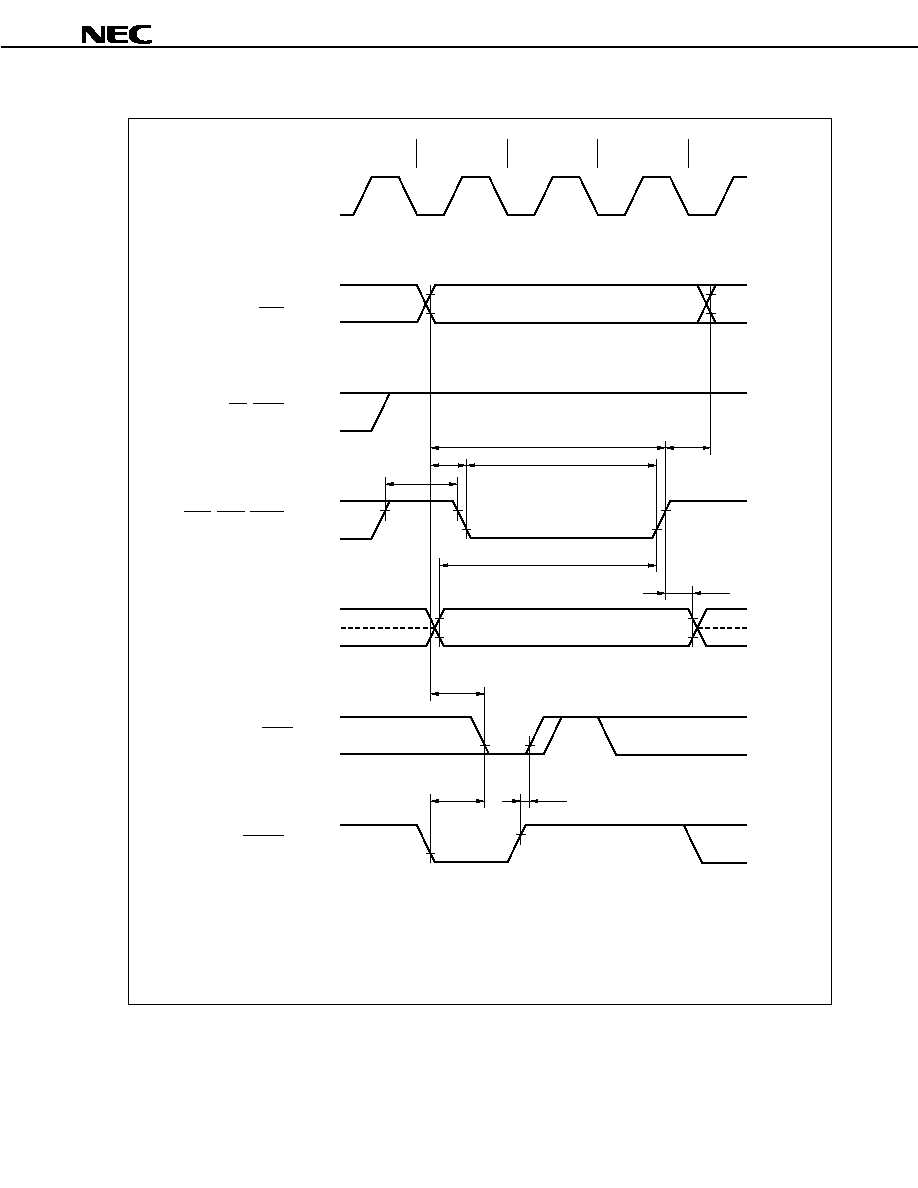
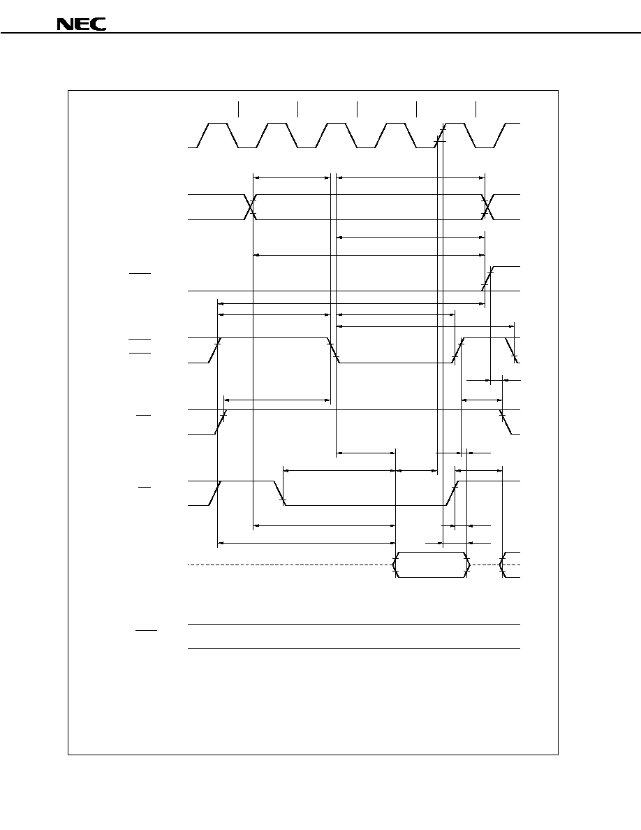
(d) DMA flyby transfer timing (SRAM
external I/O transfer) (2/2)
Remarks 1. This is the timing when the number of waits due to the DWC1 and DWC2 registers is zero and w
F
= 0.
2. The broken lines indicate high impedance.
3. n = 0, 3 to 5, m = 0 to 3
CLKOUT (Output)
T1
TW
T2
<33>
<32>
<35>
<34>
<48>
<50>
<49>
<43>
<42>
<41>
<44>
<45>
<37>
<38>
<24>
<24>
<25>
<25>
<40>
<39>
A0 to A23 (Output)
CSn (Output)
RD (Output)
DMAAKm (Output)
IORD (Output)
IOWR (Output)
UWR, LWR (Output)
D0 to D15 (I/O)
WAIT (Input)
BCYST (Output)
Preliminary Data Sheet U15390EJ1V0DS
32
µ
µ
µ
µ
PD703130
(e) DMA flyby transfer timing (external I/O
SRAM transfer) (1/2)
Parameter
Symbol
Condition
MIN.
MAX.
Unit
WAIT setup time (to CLKOUT
)
<24>
t
SWK
15
ns
WAIT hold time (from CLKOUT
)
<25>
t
HKW
2
ns
IORD low-level width
<32>
t
WRDL
(1 + w
D
+ w
F
+ w)T
≠ 10
ns
IORD high-level width
<33>
t
WRDH
T ≠ 10
ns
Delay time from address, CSn to
IORD
<34>
t
DARD
0.5T ≠ 10
ns
Delay time from IORD
to address
<35>
t
DRDA
(0.5 + i)T ≠ 10
ns
Delay time from IORD
to data output
<37>
t
DRDOD
(0.5 + i)T ≠ 10
ns
WAIT setup time (to address)
<38>
t
SAW
Note
T ≠ 25
ns
WAIT setup time (to BCYST
)
<39>
t
SBSW
Note
T ≠ 25
ns
WAIT hold time (from BCYST
)
<40>
t
HBSW
Note
0
ns
Delay time from address to UWR,
LWR
<41>
t
DAWR
0.5T ≠ 10
ns
Address setup time (to UWR, LWR
)
<42>
t
SAWR
(1.5 + w
D
+ w)T ≠ 10
ns
Delay time from UWR, LWR to
address
<43>
t
DWRA
0.5T ≠ 10
ns
UWR, LWR high-level width
<44>
t
WWRH
T ≠ 10
ns
UWR, LWR low-level width
<45>
t
WWRL
(1 + w
D
+ w)T ≠ 10
ns
w
F
= 0
0
ns
Delay time from UWR, LWR
to IORD <48>
t
DWRRD
w
F
= 1
T ≠ 10
ns
Delay time from DMAAKm
to IORD
<51>
t
DDARD
0.5T ≠ 10
ns
Delay time from IORD
to DMAAKm
<52>
t
DRDDA
0.5T ≠ 10
ns
Note For first WAIT sampling when the number of waits due to the DWC1 and DWC2 registers is zero.
Remarks 1. T = t
CYK
2. w: The number of waits due to WAIT.
3. w
D
: The number of waits due to the DWC1 and DWC2 registers.
4. w
F
: The number of waits that are inserted for a source-side access during a DMA flyby transfer.
5. i: The number of idle states that are inserted when a write cycle follows a read cycle.
6. n = 0, 3 to 5, m = 0 to 3
Preliminary Data Sheet U15390EJ1V0DS
33
µ
µ
µ
µ
PD703130
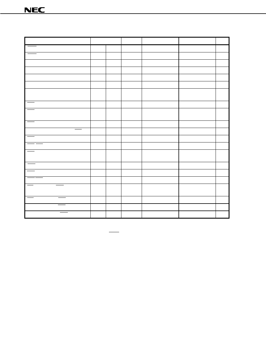
(e) DMA flyby transfer timing (external I/O
SRAM transfer) (2/2)
Remarks 1. This is the timing when the number of waits due to the DWC1 and DWC2 registers is zero and w
F
= 0.
2. The broken lines indicate high impedance.
3. n = 0, 3 to 5, m = 0 to 3
CLKOUT (Output)
T1
TW
T2
<44>
<45>
<48>
<52>
<33>
<37>
<38>
<24>
<24>
<25>
<25>
<40>
<39>
<42>
<41>
<43>
<51>
<32>
<35>
<34>
A0 to A23 (Output)
CSn (Output)
UWR, LWR (Output)
RD (Output)
DMAAKm (Output)
IOWR (Output)
IORD (Output)
D0 to D15 (I/O)
WAIT (Input)
BCYST (Output)
Preliminary Data Sheet U15390EJ1V0DS
34
µ
µ
µ
µ
PD703130
(5) Page ROM access timing (1/2)
Parameter
Symbol
Condition
MIN.
MAX.
Unit
WAIT setup time (to CLKOUT
)
<24>
t
SWK
15
ns
WAIT hold time (from CLKOUT
)
<25>
t
HKW
2
ns
Data input setup time
(to CLKOUT
)
<26>
t
SKID
18
ns
Data input hold time
(from CLKOUT
)
<27>
t
HKID
2
ns
Off-page data input setup time (to
address)
<30>
t
SAID
(1.5 + w
D
+ w)T ≠ 28
ns
Off-page data input setup time (to RD)
<31>
t
SRDID
(1 + w
D
+ w)T ≠ 32
ns
Off-page RD low-level width
<32>
t
WRDL
(1 + w
D
+ w)T ≠ 10
ns
RD high-level width
<33>
t
WRDH
0.5T ≠ 10
ns
Data input hold time (from RD)
<36>
t
HRDID
0
ns
Delay time from RD
to data output
<37>
t
DRDOD
(0.5 + i)T ≠ 10
ns
On-page RD low-level width
<53>
t
WORDL
(1.5 + w
PR
+ w)T
≠ 10
ns
On-page data input setup time
(to address)
<54>
t
SOAID
(1.5 + w
PR
+ w)T ≠ 28
ns
On-page data input setup time (to RD)
<55>
t
SORDID
(1.5 + w
PR
+ w)T ≠ 32
ns
Remarks 1. T = t
CYK
2. w: The number of waits due to WAIT.
3. w
D
: The number of waits due to the DWC1 and DWC2 registers.
4. w
PR
: The number of waits due to the PRC register.
5. i: The number of idle states that are inserted when a write cycle follows a read cycle.
6. Maintain at least one of the data input hold times, t
HKID
or t
HRDID
.
Preliminary Data Sheet U15390EJ1V0DS
35
µ
µ
µ
µ
PD703130
(5) Page ROM access timing (2/2)
Note On-page and off-page addresses are as follows.
PRC Register
MA5
MA4
MA3
On-page Addresses
Off-page Addresses
0
0
0
A0, A1
A2 to A23
0
0
1
A0 to A2
A3 to A23
0
1
1
A0 to A3
A4 to A23
1
1
1
A0 to A4
A5 to A23
Remarks 1. This is the timing for the following case.
Number of waits due to the DWC1 and DWC2 registers (TDW): 1
Number of waits due to the PRC register (TPRW): 1
2. The broken lines indicate high impedance.
3. n = 0, 3 to 5
CLKOUT (Output)
On-page address
Note
T1
TDW
TW
T2
TO1
TPRW
TW
TO2
<24>
<25>
<24>
<25>
<24>
<25>
<24>
<25>
<26>
<27>
<36>
<32>
<31>
<53>
<55>
<27>
<26>
<36>
<37>
<33>
<30>
<54>
Off-page address
Note
CSn (Output)
UWR, LWR (Output)
RD (Output)
D0 to D15 (I/O)
WAIT (Input)
BCYST (Output)
Preliminary Data Sheet U15390EJ1V0DS
36
µ
µ
µ
µ
PD703130
(6) DRAM access timing
(a) Read timing (high-speed page DRAM access, normal access: off-page) (1/3)
Parameter
Symbol
Condition
MIN.
MAX.
Unit
WAIT setup time (to CLKOUT
)
<24>
t
SWK
15
ns
WAIT hold time (from CLKOUT
)
<25>
t
HKW
2
ns
Data input setup time (to CLKOUT
)
<26>
t
SKID
18
ns
Data input hold time (from CLKOUT
)
<27>
t
HKID
2
ns
Delay time from OE
to data output
<37>
t
DRDOD
(0.5 + i)T ≠ 10
ns
Row address setup time
<56>
t
ASR
(0.5 + w
RP
)T ≠ 10
ns
Row address hold time
<57>
t
RAH
(0.5 + w
RH
)T ≠ 10
ns
Column address setup time
<58>
t
ASC
0.5T ≠ 10
ns
Column address hold time
<59>
t
CAH
(1.5 + w
DA
+ w)T ≠ 10
ns
Read/write cycle time
<60>
t
RC
(3 + w
RP
+ w
RH
+ w
DA
+ w)T
≠ 10
ns
RAS precharge time
<61>
t
RP
(0.5 + w
RP
)T ≠ 10
ns
RAS pulse time
<62>
t
RAS
(2.5 + w
RH
+ w
DA
+ w)T
≠ 10
ns
RAS hold time
<63>
t
RSH
(1.5 + w
DA
+ w)T ≠ 10
ns
Column address read time for RAS
<64>
t
RAL
(2 + w
DA
+ w)T ≠ 10
ns
CAS pulse width
<65>
t
CAS
(1 + w
DA
+ w)T ≠ 10
ns
CAS-RAS precharge time
<66>
t
CRP
(1 + w
RP
)T ≠ 10
ns
CAS hold time
<67>
t
CSH
(2 + w
RH
+ w
DA
+ w)T
≠ 10
ns
WE setup time
<68>
t
RCS
(2 + w
RP
+ w
RH
)T ≠ 10
ns
WE hold time (from RAS
)
<69>
t
RRH
0.5T ≠ 10
ns
WE hold time (from CAS
)
<70>
t
RCH
T ≠ 10
ns
CAS precharge time
<71>
t
CPN
(2 + w
RP
+ w
RH
)T ≠ 10
ns
Output enable access time
<72>
t
OEA
(2 + w
RP
+ w
RH
+ w
DA
+ w)T
≠ 28
ns
RAS access time
<73>
t
RAC
(2 + w
RH
+ w
DA
+ w)T
≠ 28
ns
Access time from column address
<74>
t
AA
(1.5 + w
DA
+ w)T ≠ 28
ns
CAS access time
<75>
t
CAC
(1 + w
DA
+ w)T ≠ 28
ns
Remarks 1. T = t
CYK
2. w: The number of waits due to WAIT.
3. w
RP
: The number of waits due to the RPCxx bit of the DRCn register (n = 0 to 3, xx = 00 to 03, 10 to
13).
4. w
RH
: The number of waits due to the RHCxx bit of the DRCn register (n = 0 to 3, xx = 00 to 03, 10 to
13).
5. w
DA
: The number of waits due to the DACxx bit of the DRCn register (n = 0 to 3, xx = 00 to 03, 10 to
13).
6. i: The number of idle states that are inserted when a write cycle follows a read cycle.
Preliminary Data Sheet U15390EJ1V0DS
37
µ
µ
µ
µ
PD703130
(a) Read timing (high-speed page DRAM access, normal access: off-page) (2/3)
Parameter
Symbol
Condition
MIN.
MAX.
Unit
RAS column address delay time
<76>
t
RAD
(0.5 + w
RH
)T ≠ 10
ns
RAS-CAS delay time
<77>
t
RCD
(1 + w
RH
)T ≠ 10
ns
Output buffer turn-off delay time (from
OE
)
<78>
t
OEZ
0
ns
Output buffer turn-off delay time (from
CAS
)
<79>
t
OFF
0
ns
Remarks 1. T = t
CYK
2. w
RH
: The number of waits due to the RHCxx bit of the DRCn register (n = 0 to 3, xx = 00 to 03, 10 to
13).
Preliminary Data Sheet U15390EJ1V0DS
38
µ
µ
µ
µ
PD703130
(a) Read timing (high-speed page DRAM access, normal access: off-page) (3/3)
Remarks 1. This is the timing for the following case (n = 0 to 3, xx = 00 to 03, 10 to 13).
Number of waits due to the RPCxx bit of the DRCn register (TRPW): 1
Number of waits due to the RHCxx bit of the DRCn register (TRHW): 1
Number of waits due to the DACxx bit of the DRCn register (TDAW): 1
2. The broken lines indicate high impedance.
3. n = 3 to 5
TRPW
TRHW
T2
T1
TDAW
TW
T3
<56>
<61>
<57>
<58>
<59>
<62>
<76>
<63>
<64>
<60>
<77>
<65>
<67>
<66>
<71>
<73>
<68>
<75>
<74>
<72>
<70>
<69>
<79>
<37>
<27>
<25>
<26>
<25>
<24>
<78>
<24>
CLKOUT (Output)
A0 to A23 (Output)
RASn (Output)
WE (Output)
OE (Output)
WAIT (Input)
D0 to D15 (I/O)
UCAS (Output)
LCAS (Output)
Row address
Column address

Preliminary Data Sheet U15390EJ1V0DS
39
µ
µ
µ
µ
PD703130
[MEMO]
Preliminary Data Sheet U15390EJ1V0DS
40
µ
µ
µ
µ
PD703130
(b) Read timing (high-speed page DRAM access: on-page) (1/2)
Parameter
Symbol
Condition
MIN.
MAX.
Unit
Data input setup time (to CLKOUT
)
<26>
t
SKID
18
ns
Data input hold time (from CLKOUT
)
<27>
t
HKID
2
ns
Delay time from OE
to data output
<37>
t
DRDOD
(0.5 + i)T ≠ 10
ns
Column address setup time
<58>
t
ASC
(0.5 + w
CP
)T ≠ 10
ns
Column address hold time
<59>
t
CAH
(1.5 + w
DA
)T ≠ 10
ns
RAS hold time
<63>
t
RSH
(1.5 + w
DA
)T ≠ 10
ns
Column address read time for RAS
<64>
t
RAL
(2 + w
CP
+ w
DA
)T ≠ 10
ns
CAS pulse width
<65>
t
CAS
(1 + w
DA
)T ≠ 10
ns
WE setup time (to CAS
)
<68>
t
RCS
(1 + w
CP
)T ≠ 10
ns
WE hold time (from RAS
)
<69>
t
RRH
0.5T ≠ 10
ns
WE hold time (from CAS
)
<70>
t
RCH
T ≠ 10
ns
Output enable access time
<72>
t
OEA
(1 + w
CP
+ w
DA
)T ≠ 28
ns
Access time from column address
<74>
t
AA
(1.5 + w
CP
+ w
DA
)T ≠ 28
ns
CAS access time
<75>
t
CAC
(1 + w
DA
)T ≠ 28
ns
Output buffer turn-off delay time (from
OE
)
<78>
t
OEZ
0
ns
Output buffer turn-off delay time (from
CAS
)
<79>
t
OFF
0
ns
Access time from CAS precharge
<80>
t
ACP
(2 + w
CP
+ w
DA
)T ≠ 28
ns
CAS precharge time
<81>
t
CP
(1 + w
CP
)T ≠ 10
ns
High-speed page mode cycle time
<82>
t
PC
(2 + w
CP
+ w
DA
)T ≠ 10
ns
RAS hold time for CAS precharge
<83>
t
RHCP
(2.5 + w
CP
+ w
DA
)T ≠ 10
ns
Remarks 1. T = t
CYK
2. w
CP
: The number of waits due to the CPCxx bit of the DRCn register (n = 0 to 3, xx = 00 to 03, 10 to
13).
3. w
DA
: The number of waits due to the DACxx bit of the DRCn register (n = 0 to 3, xx = 00 to 03, 10 to
13).
4. i: The number of idle states that are inserted when a write cycle follows a read cycle.
Preliminary Data Sheet U15390EJ1V0DS
41
µ
µ
µ
µ
PD703130
(b) Read timing (high-speed page DRAM access: on-page) (2/2)
Remarks 1. This is the timing for the following case (n = 0 to 3, xx = 00 to 03, 10 to 13).
Number of waits due to the CPCxx bit of the DRCn register (TCPW): 1
Number of waits due to the DACxx bit of the DRCn register (TDAW): 1
2. The broken lines indicate high impedance.
3. n = 3 to 5
TCPW
TO1
TDAW
TO2
<58>
<59>
<63>
<64>
<83>
<65>
<81>
<82>
<68>
<75>
<72>
<26>
<79>
<37>
<74>
<80>
<27>
<78>
<70>
<69>
CLKOUT (Output)
A0 to A23 (Output)
RASn (Output)
UCAS (Output)
LCAS (Output)
WE (Output)
OE (Output)
D0 to D15 (I/O)
WAIT (Input)
Column address
Preliminary Data Sheet U15390EJ1V0DS
42
µ
µ
µ
µ
PD703130
(c) Write timing (high-speed page DRAM access, normal access: off-page) (1/2)
Parameter
Symbol
Condition
MIN.
MAX.
Unit
WAIT setup time (to CLKOUT
)
<24>
t
SWK
15
ns
WAIT hold time (from CLKOUT
)
<25>
t
HKW
2
ns
Row address setup time
<56>
t
ASR
(0.5 + w
RP
)T ≠ 10
ns
Row address hold time
<57>
t
RAH
(0.5 + w
RH
)T ≠ 10
ns
Column address setup time
<58>
t
ASC
0.5T ≠ 10
ns
Column address hold time
<59>
t
CAH
(1.5 + w
DA
+ w)T ≠ 10
ns
Read/write cycle time
<60>
t
RC
(3 + w
RP
+ w
RH
+ w
DA
+ w)T
≠ 10
ns
RAS precharge time
<61>
t
RP
(0.5 + w
RP
)T ≠ 10
ns
RAS pulse time
<62>
t
RAS
(2.5 + w
RH
+ w
DA
+ w)T
≠ 10
ns
RAS hold time
<63>
t
RSH
(1.5 + w
DA
+ w)T ≠ 10
ns
Column address read time (from RAS
)
<64>
t
RAL
(2 + w
DA
+ w)T ≠ 10
ns
CAS pulse width
<65>
t
CAS
(1 + w
DA
+ w)T ≠ 10
ns
CAS-RAS precharge time
<66>
t
CRP
(1 + w
RH
)T ≠ 10
ns
CAS hold time
<67>
t
CSH
(2 + w
RH
+ w
DA
+ w)T
≠ 10
ns
CAS precharge time
<71>
t
CPN
(2 + w
RP
+ w
RH
)T ≠ 10
ns
RAS column address delay time
<76>
t
RAD
(0.5 + w
RH
)T ≠ 10
ns
RAS-CAS delay time
<77>
t
RCD
(1 + w
RH
)T ≠ 10
ns
WE setup time (to CAS
)
<84>
t
WCS
(1 + w
RP
+ w
RH
)T
≠ 10
ns
WE hold time (from CAS
)
<85>
t
WCH
(1 + w
DA
+ w)T ≠ 10
ns
Data setup time (to CAS
)
<86>
t
DS
(1.5 + w
RP
+ w
RH
)T ≠ 10
ns
Data hold time (from CAS
)
<87>
t
DH
(1.5 + w
DA
+ w)T ≠ 10
ns
Remarks 1. T = t
CYK
2. w: The number of waits due to WAIT.
3. w
RP
: The number of waits due to the RPCxx bit of the DRCn register (n = 0 to 3, xx = 00 to 03, 10 to
13).
4. w
RH
: The number of waits due to the RHCxx bit of the DRCn register (n = 0 to 3, xx = 00 to 03, 10 to
13).
5. w
DA
: The number of waits due to the DACxx bit of the DRCn register (n = 0 to 3, xx = 00 to 03, 10 to
13).
Preliminary Data Sheet U15390EJ1V0DS
43
µ
µ
µ
µ
PD703130
(c) Write timing (high-speed page DRAM access, normal access: off-page) (2/2)
Remarks 1. This is the timing for the following case (n = 0 to 3, xx = 00 to 03, 10 to 13).
Number of waits due to the RPCxx bit of the DRCn register (TRPW): 1
Number of waits due to the RHCxx bit of the DRCn register (TRHW): 1
Number of waits due to the DACxx bit of the DRCn register (TDAW): 1
2. The broken lines indicate high impedance.
3. n = 3 to 5
TRPW
TRHW
T2
T1
TDAW
TW
T3
<56>
<61>
<57>
<58>
<59>
<62>
<76>
<63>
<64>
<60>
<77>
<65>
<67>
<66>
<71>
<84>
<25>
<25>
<24>
<24>
<85>
<86>
<87>
CLKOUT (Output)
A0 to A23 (Output)
RASn (Output)
UCAS (Output)
LCAS (Output)
WE (Output)
OE (Output)
D0 to D15 (I/O)
WAIT (Input)
Row address
Column address
Preliminary Data Sheet U15390EJ1V0DS
44
µ
µ
µ
µ
PD703130
(d) Write timing (high-speed page DRAM access: on-page) (1/2)
Parameter
Symbol
Condition
MIN.
MAX.
Unit
Column address setup time
<58>
t
ASC
(0.5 + w
CP
)T ≠ 10
ns
Column address hold time
<59>
t
CAH
(1.5 + w
DA
)T ≠ 10
ns
RAS hold time
<63>
t
RSH
(1.5 + w
DA
)T ≠ 10
ns
Column address read time (from RAS
)
<64>
t
RAL
(2 + w
CP
+ w
DA
)T ≠ 10
ns
CAS pulse width
<65>
t
CAS
(1 + w
DA
)T ≠ 10
ns
CAS precharge time
<81>
t
CP
(1 + w
CP
)T ≠ 10
ns
RAS hold time for CAS precharge
<83>
t
RHCP
(2.5 + w
CP
+ w
DA
)T
≠ 10
ns
WE setup time (to CAS
)
<84>
t
WCS
w
CP
1
w
CP
T ≠ 10
ns
WE hold time (from CAS
)
<85>
t
WCH
(1 + w
DA
)T ≠ 10
ns
Data setup time (to CAS
)
<86>
t
DS
(0.5 + w
CP
)T ≠ 10
ns
Data hold time (from CAS
)
<87>
t
DH
(1.5 + w
DA
)T ≠ 10
ns
WE read time (from RAS
)
<88>
t
RWL
w
CP
= 0
(1.5 + w
DA
)T ≠ 10
ns
WE read time (from CAS
)
<89>
t
CWL
w
CP
= 0
(1 + w
DA
)T ≠ 10
ns
Data setup time (to WE
)
<90>
t
DSWE
w
CP
= 0
0.5T ≠ 10
ns
Data hold time (from WE
)
<91>
t
DHWE
w
CP
= 0
(1.5 + w
DA
)T ≠ 10
ns
WE pulse width
<92>
t
WP
w
CP
= 0
(1 + w
DA
)T ≠ 10
ns
Remarks 1. T = t
CYK
2. w
CP
: The number of waits due to the CPCxx bit of the DRCn register (n = 0 to 3, xx = 00 to 03, 10 to
13).
3. w
DA
: The number of waits due to the DACxx bit of the DRCn register (n = 0 to 3, xx = 00 to 03, 10 to
13).
Preliminary Data Sheet U15390EJ1V0DS
45
µ
µ
µ
µ
PD703130
(d) Write timing (high-speed page DRAM access: on-page) (2/2)
TCPW
TO1
TDAW
TO2
<58>
<59>
<63>
<64>
<83>
<81>
<65>
<89>
<88>
<84>
<85>
<92>
<91>
<86>
<87>
<90>
CLKOUT (Output)
A0 to A23 (Output)
RASn (Output)
UCAS (Output)
LCAS (Output)
OE (Output)
WE (Output)
D0 to D15 (I/O)
WAIT (Input)
Column address
Remarks 1. This is the timing for the following case (n = 0 to 3, xx = 00 to 03, 10 to 13).
Number of waits due to the CPCxx bit of the DRCn register (TCPW ): 1
Number of waits due to the DACxx bit of the DRCn register (TDAW): 1
2. The broken lines indicate high impedance.
3. n = 3 to 5
Preliminary Data Sheet U15390EJ1V0DS
46
µ
µ
µ
µ
PD703130
(e) Read timing (EDO DRAM) (1/3)
Parameter
Symbol
Condition
MIN.
MAX.
Unit
Data input setup time (to CLKOUT
)
<26>
t
SKID
18
ns
Data input hold time (from CLKOUT
)
<27>
t
HKID
2
ns
Delay time from OE
to data output
<37>
t
DRDOD
(0.5 + i)T ≠ 10
ns
Row address setup time
<56>
t
ASR
(0.5 + w
RP
)T ≠ 10
ns
Row address hold time
<57>
t
RAH
(0.5 + w
RH
)T ≠ 10
ns
Column address setup time
<58>
t
ASC
0.5T ≠ 10
ns
Column address hold time
<59>
t
CAH
(0.5 + w
DA
)T ≠ 10
ns
RAS precharge time
<61>
t
RP
(0.5 + w
RP
)T ≠ 10
ns
Column address read time (from RAS
)
<64>
t
RAL
(2 + w
CP
+ w
DA
)T ≠ 10
ns
CAS-RAS precharge time
<66>
t
CRP
(1 + w
RP
)T ≠ 10
ns
CAS hold time
<67>
t
CSH
(1.5 + w
RH
+ w
DA
)T ≠ 10
ns
WE setup time (to CAS
)
<68>
t
RCS
(2 + w
RP
+ w
RH
)T ≠ 10
ns
WE hold time (from RAS
)
<69>
t
RRH
0.5T ≠ 10
ns
WE hold time (from CAS
)
<70>
t
RCH
1.5T ≠ 10
ns
RAS access time
<73>
t
RAC
(2 + w
RH
+ w
DA
)T ≠ 28
ns
Access time from column address
<74>
t
AA
(1.5 + w
DA
)T ≠ 28
ns
CAS access time
<75>
t
CAC
(1 + w
DA
)T ≠ 28
ns
Delay time from RAS to column address
<76>
t
RAD
(0.5 + w
RH
)T ≠ 10
ns
RAS-CAS delay time
<77>
t
RCD
(1 + w
RH
)T ≠ 10
ns
Output buffer turn-off delay time (from
OE)
<78>
t
OEZ
0
ns
Access time from CAS precharge
<80>
t
ACP
(1.5 + w
CP
+ w
DA
)T ≠ 28
ns
CAS precharge time
<81>
t
CP
(0.5 + w
CP
)T ≠ 10
ns
RAS hold time for CAS precharge
<83>
t
RHCP
(2 + w
CP
+ w
DA
)T ≠ 10
ns
Read cycle time
<93>
t
HPC
(1 + w
DA
+ w
CP
)T ≠ 10
ns
RAS pulse width
<94>
t
RASP
(2.5 + w
RH
+ w
DA
)T ≠ 10
ns
CAS pulse width
<95>
t
HCAS
(0.5 + w
DA
)T ≠ 10
ns
Off-page
<96>
t
OCH1
(2 + w
RH
+ w
DA
)T ≠ 10
ns
CAS hold time from OE
On-page
<97>
t
OCH2
(0.5 + w
DA
)T ≠ 10
ns
Data input hold time (from CAS
)
<98>
t
DHC
0
ns
Remarks 1. T = t
CYK
2. w
RP
: The number of waits due to the RPCxx bit of the DRCn register (n = 0 to 3, xx = 00 to 03, 10 to
13).
3. w
RH
: The number of waits due to the RHCxx bit of the DRCn register (n = 0 to 3, xx = 00 to 03, 10 to
13).
4. w
DA
: The number of waits due to the DACxx bit of the DRCn register (n = 0 to 3, xx = 00 to 03, 10 to
13).
5. w
CP
: The number of waits due to the CPCxx bit of the DRCn register (n = 0 to 3, xx = 00 to 03, 10 to
13).
6. i: The number of idle states that are inserted when a write cycle follows a read cycle.
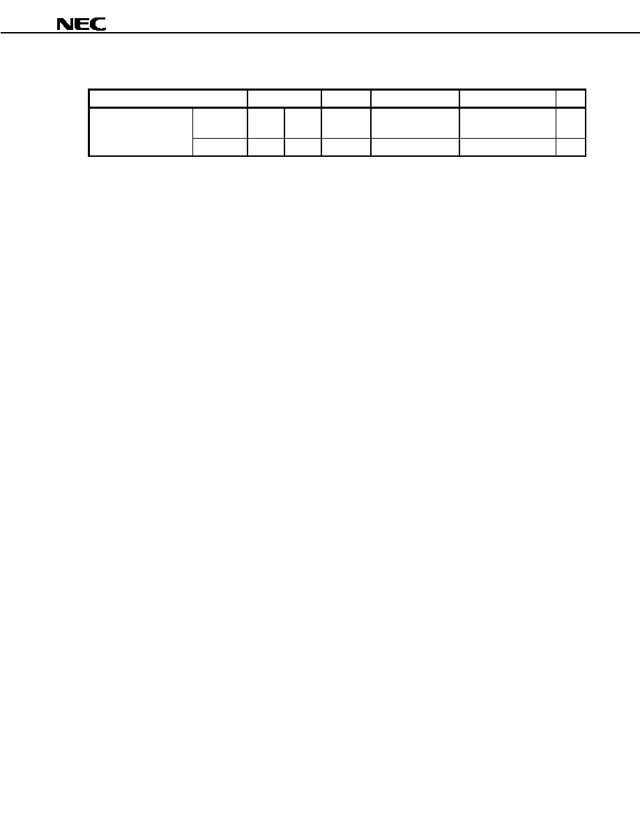
Preliminary Data Sheet U15390EJ1V0DS
47
µ
µ
µ
µ
PD703130
(e) Read timing (EDO DRAM) (2/3)
Parameter
Symbol
Condition
MIN.
MAX.
Unit
Off-page
<99>
t
OEA1
(2 + w
RP
+ w
RH
+ w
DA
)T
≠ 28
ns
Output enable access
time
On-page
<100>
t
OEA2
(1 + w
CP
+ w
DA
)T ≠ 28
ns
Remarks 1. T = t
CYK
2. w
RP
: The number of waits due to the RPCxx bit of the DRCn register (n = 0 to 3, xx = 00 to 03, 10 to
13).
3. w
RH
: The number of waits due to the RHCxx bit of the DRCn register (n = 0 to 3, xx = 00 to 03, 10
to 13).
4. w
DA
: The number of waits due to the DACxx bit of the DRCn register (n = 0 to 3, xx = 00 to 03, 10 to
13).
5. w
CP
: The number of waits due to the CPCxx bit of the DRCn register (n = 0 to 3, xx = 00 to 03, 10 to
13).
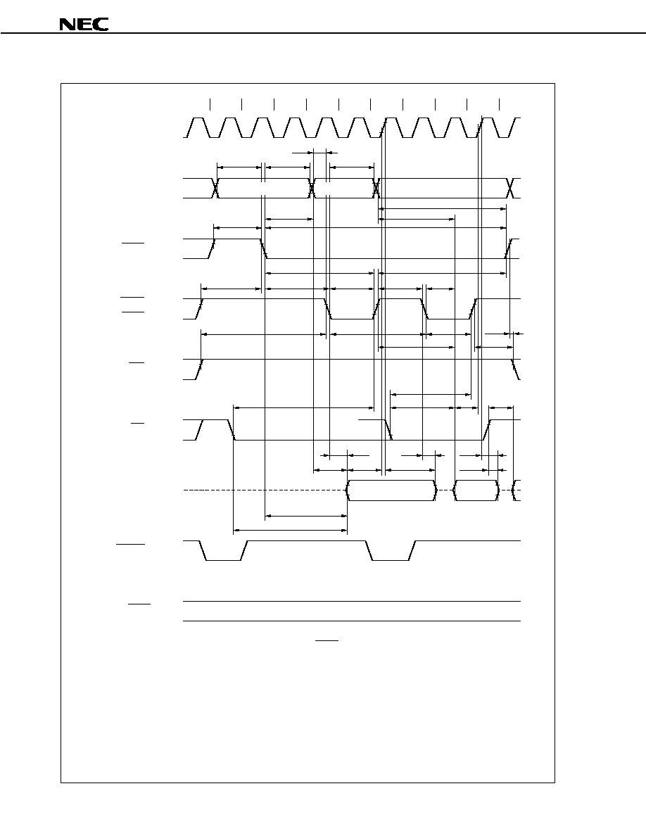
Preliminary Data Sheet U15390EJ1V0DS
48
µ
µ
µ
µ
PD703130
(e) Read timing (EDO DRAM) (3/3)
Note For on-page access from another cycle during the RASn low-level signal.
Remarks 1. This is the timing for the following case (n = 0 to 3, xx = 00 to 03, 10 to 13).
Number of waits due to the RPCxx bit of the DRCn register (TRPW): 1
Number of waits due to the RHCxx bit of the DRCn register (TRHW): 1
Number of waits due to the DACxx bit of the DRCn register (TDAW): 1
Number of waits due to the CPCxx bit of the DRCn register (TCPW): 1
2. The broken lines indicate high impedance.
3. n = 3 to 5
TRPW
T1
TRHW
T2
TDAW TCPW
TB
TDAW
TE
<56>
<57>
<59>
<58>
<76>
<64>
<94>
<61>
<67>
<83>
<77>
<95>
<81>
<75>
<66>
<93>
<95>
<80>
<97>
<74>
<27>
<78>
Data
<74>
Data
<70>
<69>
<68>
<96>
<100>
<26>
<37>
<27>
<98>
<26>
<75>
<73>
<99>
CLKOUT (Output)
A0 to A23 (Output)
RASn (Output)
UCAS (Output)
LCAS (Output)
WE (Output)
OE (Output)
D0 to D15 (I/O)
BCYST (Output)
WAIT (Input)
Row address
Column address
Column address
Note

Preliminary Data Sheet U15390EJ1V0DS
49
µ
µ
µ
µ
PD703130
[MEMO]
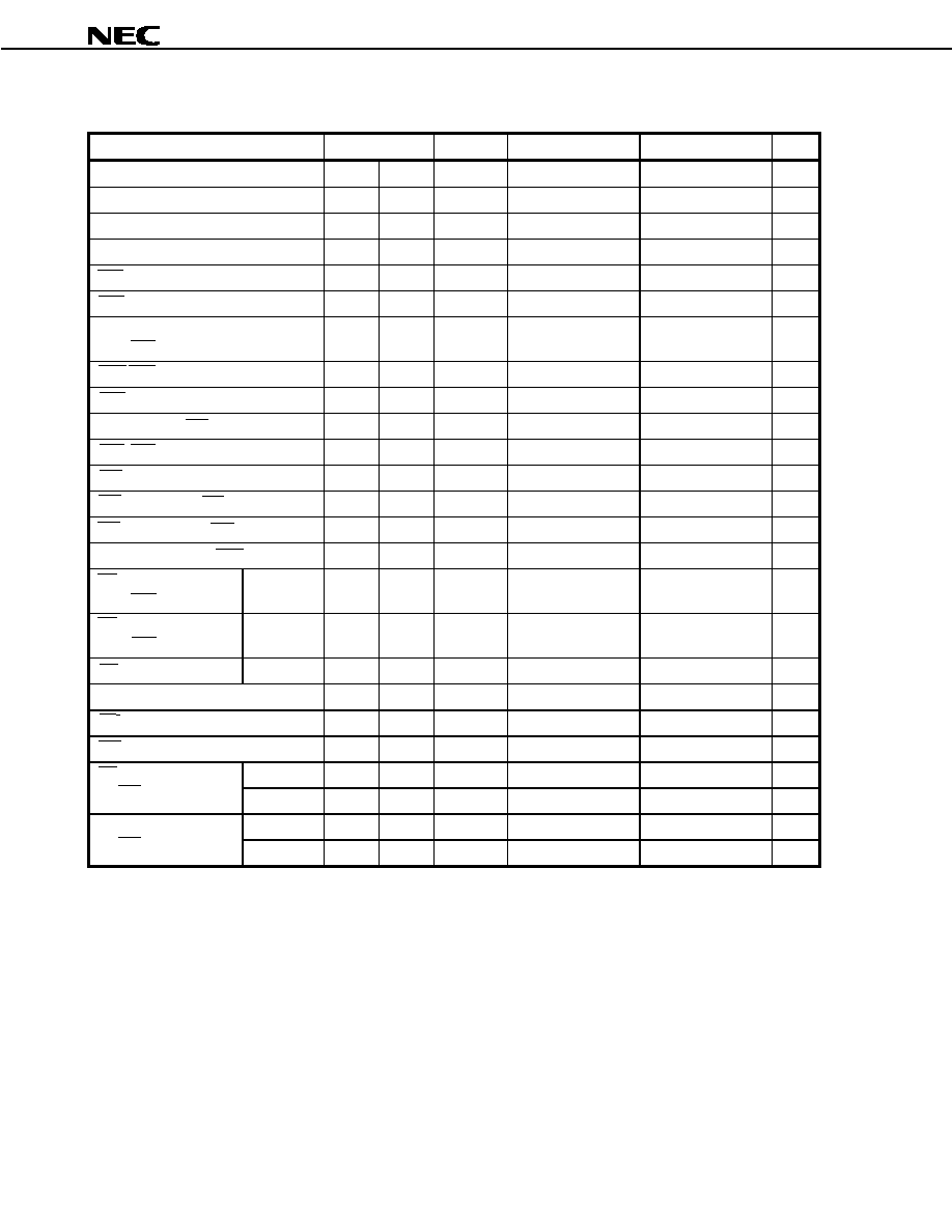
Preliminary Data Sheet U15390EJ1V0DS
50
µ
µ
µ
µ
PD703130
(f) Write timing (EDO DRAM) (1/2)
Parameter
Symbol
Condition
MIN.
MAX.
Unit
Row address setup time
<56>
t
ASR
(0.5 + w
RP
)T ≠ 10
ns
Row address hold time
<57>
t
RAH
(0.5 + w
RH
)T ≠ 10
ns
Column address setup time
<58>
t
ASC
0.5T ≠ 10
ns
Column address hold time
<59>
t
CAH
(0.5 + w
DA
)T ≠ 10
ns
RAS precharge time
<61>
t
RP
(0.5 + w
RP
)T ≠ 10
ns
RAS hold time
<63>
t
RSH
(1.5 + w
DA
)T ≠ 10
ns
Column address read time
(from RAS
)
<64>
t
RAL
(2 + w
CP
+ w
DA
)T ≠ 10
ns
CAS-RAS precharge time
<66>
t
CRP
(1 + w
RP
)T ≠ 10
ns
CAS hold time
<67>
t
CSH
(1.5 + w
RH
+ w
DA
)T ≠ 10
ns
Delay time from RAS to column address
<76>
t
RAD
(0.5 + w
RH
)T ≠ 10
ns
RAS-CAS delay time
<77>
t
RCD
(1 + w
RH
)T ≠ 10
ns
CAS precharge time
<81>
t
CP
(0.5 + w
CP
)T ≠ 10
ns
RAS hold time for CAS precharge
<83>
t
RHCP
(2 + w
CP
+ w
DA
)T ≠ 10
ns
WE hold time (from CAS
)
<85>
t
WCH
(1 + w
DA
)T ≠ 10
ns
Data hold time (from CAS
)
<87>
t
DH
(0.5 + w
DA
)T ≠ 10
ns
WE read time
(from RAS
)
On-page
<88>
t
RWL
w
CP
= 0
(1.5 + w
DA
)T ≠ 10
ns
WE read time
(from CAS
)
On-page
<89>
t
CWL
w
CP
= 0
(0.5 + w
DA
)T ≠ 10
ns
WE pulse width
On-page
<92>
t
WP
w
CP
= 0
(1 + w
DA
)T ≠ 10
ns
Write cycle time
<93>
t
HPC
(1 + w
DA
+ w
CP
)T ≠ 10
ns
RAS pulse width
<94>
t
RASP
(2.5 + w
RH
+ w
DA
)T ≠ 10
ns
CAS pulse width
<95>
t
HCAS
(0.5 + w
DA
)T ≠ 10
ns
Off-page
<101>
t
WCS1
(1 + w
RP
+ w
RH
)T ≠ 10
ns
WE setup time
(to CAS
)
On-page
<102>
t
WCS2
w
CP
1
w
CP
T ≠ 10
ns
Off-page
<103>
t
DS1
(1.5 + w
RP
+ w
RH
)T ≠ 10
ns
Data setup time
(to CAS
)
On-page
<104>
t
DS2
(0.5 + w
CP
)T ≠ 10
ns
Remarks 1. T = t
CYK
2. w
RP
: The number of waits due to the RPCxx bit of the DRCn register (n = 0 to 3, xx = 00 to 03, 10 to
13).
3. w
RH
: The number of waits due to the RHCxx bit of the DRCn register (n = 0 to 3, xx = 00 to 03, 10 to
13).
4. w
DA
: The number of waits due to the DACxx bit of the DRCn register (n = 0 to 3, xx = 00 to 03, 10 to
13).
5. w
CP
: The number of waits due to the CPCxx bit of the DRCn register (n = 0 to 3, xx = 00 to 03, 10 to
13).
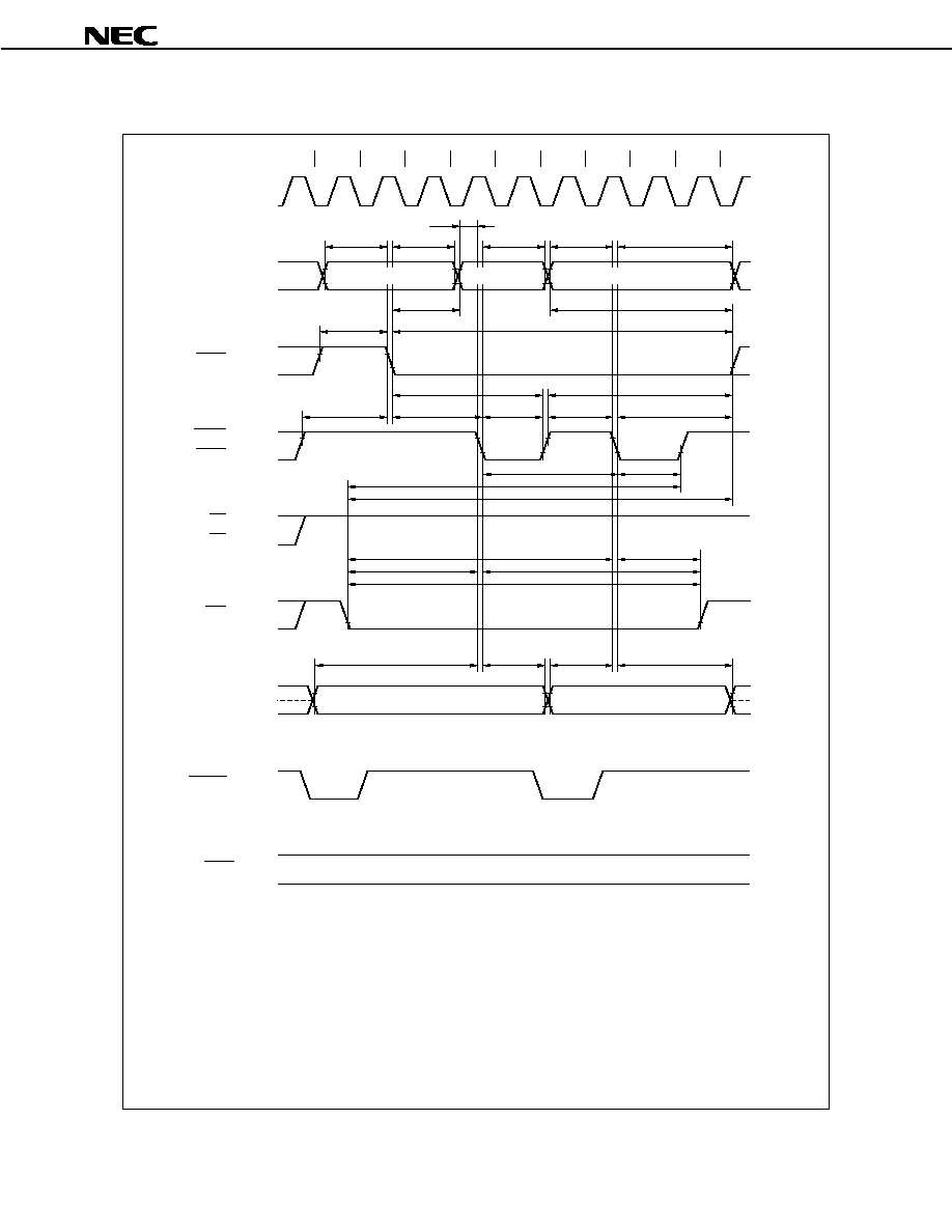
Preliminary Data Sheet U15390EJ1V0DS
51
µ
µ
µ
µ
PD703130
(f) Write timing (EDO DRAM) (2/2)
Remarks 1. This is the timing for the following case (n = 0 to 3, xx = 00 to 03, 10 to 13).
Number of waits due to the RPCxx bit of the DRCn register (TRPW): 1
Number of waits due to the RHCxx bit of the DRCn register (TRHW): 1
Number of waits due to the DACxx bit of the DRCn register (TDAW): 1
Number of waits due to the CPCxx bit of the DRCn register (TCPW): 1
2. The broken lines indicate high impedance.
3. n = 3 to 5
TRPW
T1
TRHW
T2
TDAW
TCPW
TB
TDAW
TE
<56>
<57>
<59>
<58>
<58>
<59>
<76>
<64>
<94>
<61>
<67>
<83>
<77>
<95>
<81>
<63>
<66>
<93>
<95>
<89>
<88>
<102>
<101>
<92>
<85>
<85>
<103>
<87>
<104>
<87>
Data
Data
CLKOUT (Output)
A0 to A23 (Output)
RASn (Output)
UCAS (Output)
LCAS (Output)
RD (Output)
OE (Output)
WE (Output)
D0 to D15 (I/O)
BCYST (Output)
WAIT (Input)
Row address
Column address
Column address
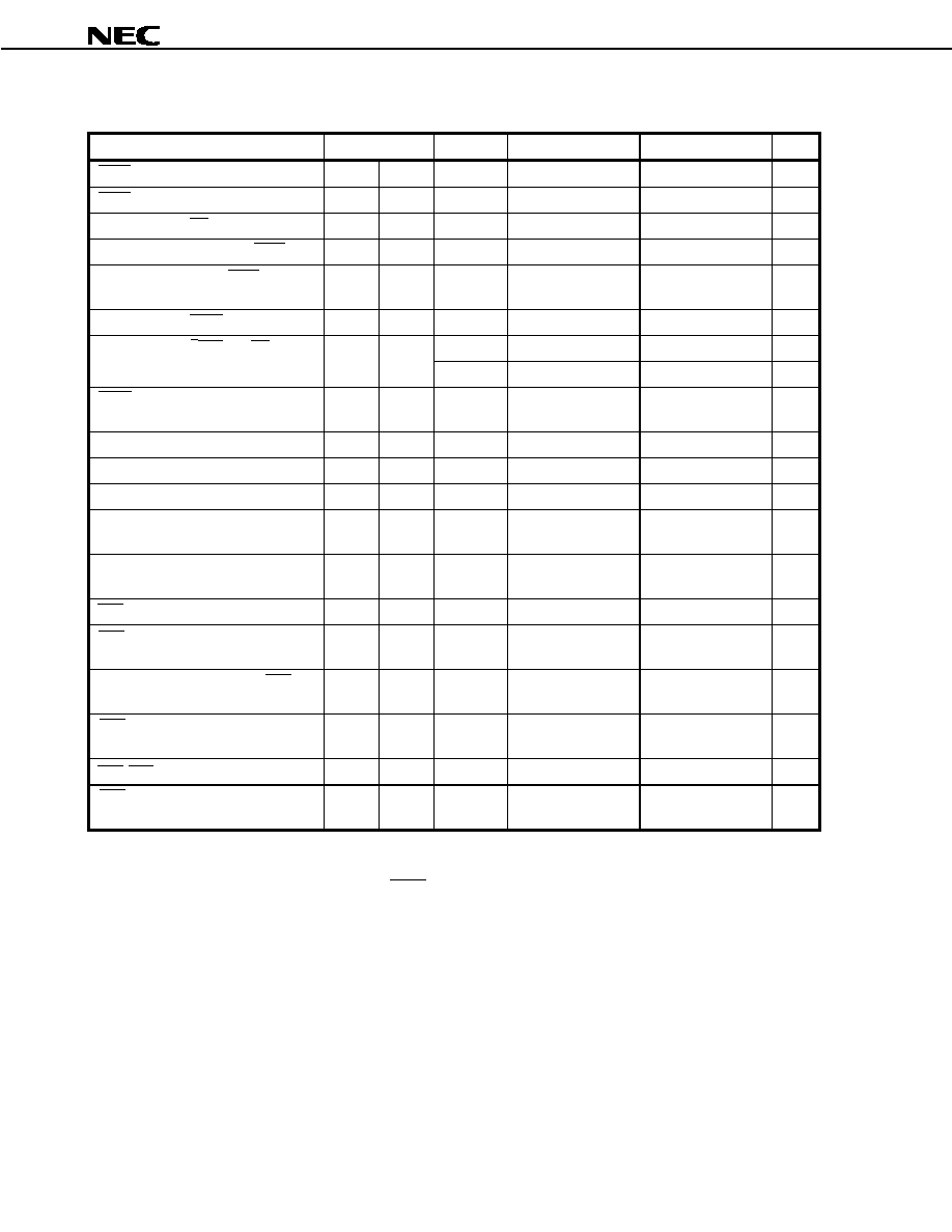
Preliminary Data Sheet U15390EJ1V0DS
52
µ
µ
µ
µ
PD703130
(g) DMA flyby transfer timing (DRAM (EDO, high-speed page)
external I/O transfer) (1/3)
Parameter
Symbol
Condition
MIN.
MAX.
Unit
WAIT setup time (to CLKOUT
)
<24>
t
SWK
15
ns
WAIT hold time (from CLKOUT
)
<25>
t
HKW
2
ns
Delay time from OE
to data output
<37>
t
DRDOD
(0.5 + i)T ≠ 10
ns
Delay time from address to IOWR
<41>
t
DAWR
(0.5 + w
RP
)T ≠ 10
ns
Address setup time (to IOWR
)
<42>
t
SAWR
(2 + w
RP
+ w
RH
+ w
DA
+
w)T ≠ 10
ns
Delay time from IOWR
to address
<43>
t
DWRA
0.5T ≠ 10
ns
w
F
= 0
0
ns
Delay time from IOWR
to RD
<48>
t
DWRRD
w
F
= 1
T ≠ 10
ns
IOWR low-level width
<50>
t
WWRL
(2 + w
RH
+ w
DA
+ w)T
≠ 10
ns
Row address setup time
<56>
t
ASR
(0.5 + w
RP
)T ≠ 10
ns
Row address hold time
<57>
t
RAH
(0.5 + w
RH
)T ≠ 10
ns
Column address setup time
<58>
t
ASC
0.5T ≠ 10
ns
Column address hold time
<59>
t
CAH
(1.5 + w
DA
+ w
F
+ w)T
≠ 10
ns
Read/write cycle time
<60>
t
RC
(3 + w
RP
+ w
RH
+ w
DA
+
w
F
+ w)T ≠ 10
ns
RAS precharge time
<61>
t
RP
(0.5 + w
RP
)T ≠ 10
ns
RAS hold time
<63>
t
RSH
(1.5 + w
DA
+ w
F
+ w)T
≠ 10
ns
Column address read time for RAS
<64>
t
RAL
(2 + w
CP
+ w
DA
+ w
F
+
w)T ≠ 10
ns
CAS pulse width
<65>
t
CAS
(1 + w
DA
+ w
F
+ w)T
≠ 10
ns
CAS-RAS precharge time
<66>
t
CRP
(1 + w
RP
)T ≠ 10
ns
CAS hold time
<67>
t
CSH
(2 + w
RH
+ w
DA
+ w
F
+
w)T ≠ 10
ns
Remarks 1. T = t
CYK
2. w: The number of waits due to WAIT.
3. w
RP
: The number of waits due to the RPCxx bit of the DRCn register (n = 0 to 3, xx = 00 to 03, 10 to
13).
4. w
RH
: The number of waits due to the RHCxx bit of the DRCn register (n = 0 to 3, xx = 00 to 03, 10 to
13).
5. w
DA
: The number of waits due to the DACxx bit of the DRCn register (n = 0 to 3, xx = 00 to 03, 10 to
13).
6. w
CP
: The number of waits due to the CPCxx bit of the DRCn register (n = 0 to 3, xx = 00 to 03, 10 to
13).
7. w
F
: The number of waits that are inserted for a source-side access during a DMA flyby transfer.
8. i: The number of idle states that are inserted when a write cycle follows a read cycle.
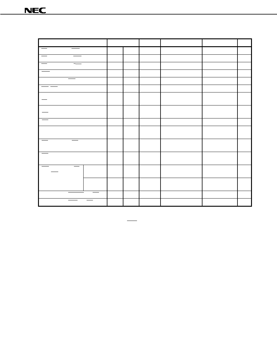
Preliminary Data Sheet U15390EJ1V0DS
53
µ
µ
µ
µ
PD703130
(g) DMA flyby transfer timing (DRAM (EDO, high-speed page)
external I/O transfer) (2/3)
Parameter
Symbol
Condition
MIN.
MAX.
Unit
WE setup time (to CAS
)
<68>
t
RCS
(2 + w
RP
+ w
RH
)T ≠ 10
ns
WE hold time (from RAS
)
<69>
t
RRH
0.5T ≠ 10
ns
WE hold time (from CAS
)
<70>
t
RCH
1.5T ≠ 10
ns
CAS precharge time
<71>
t
CPN
(2 + w
RP
+ w
RH
)T ≠ 10
ns
Delay time from RAS to column address
<76>
t
RAD
(0.5 + w
RH
)T ≠ 10
ns
RAS-CAS delay time
<77>
t
RCD
(1 + w
RH
)T ≠ 10
ns
Output buffer turn-off delay time (from
OE
)
<78>
t
OEZ
0
ns
Output buffer turn-off delay time (from
CAS
)
<79>
t
OFF
0
ns
CAS precharge time
<81>
t
CP
(0.5 + w
CP
)T ≠ 10
ns
High-speed page mode cycle time
<82>
t
PC
(2 + w
CP
+ w
DA
+ w
F
+ w)T
≠ 10
ns
RAS hold time for CAS precharge
<83>
t
RHCP
(2.5 + w
CP
+ w
DA
+ w
F
+ w)T
≠ 10
ns
RAS pulse width
<94>
t
RASP
(2.5 + w
RH
+ w
DA
+ w
F
+ w)T
≠ 10
ns
Off-page
<96>
t
OCH1
(2.5 + w
RP
+ w
RH
+ w
DA
+
w
F
+ w)T ≠ 10
ns
CAS hold time from OE
(from CAS
)
On-page
<97>
t
OCH2
(1.5 + w
CP
+ w
DA
+ w
F
+ w)T
≠ 10
ns
Delay time from DMAAKm
to CAS
<105>
t
DDACS
(1.5 + w
RH
)T ≠ 10
ns
Delay time from IOWR
to CAS
<106>
t
DRDCS
(1 + w
RH
)T ≠ 10
ns
Remarks 1. T = t
CYK
2. w: The number of waits due to WAIT.
3. w
CP
: The number of waits due to the CPCxx bit of the DRCn register (n = 0 to 3, xx = 00 to 03, 10 to
13).
4. w
DA
: The number of waits due to the DACxx bit of the DRCn register (n = 0 to 3, xx = 00 to 03, 10 to
13).
5. w
RH
: The number of waits due to the RHCxx bit of the DRCn register (n = 0 to 3, xx = 00 to 03, 10 to
13).
6. w
RP
: The number of waits due to the RPCxx bit of the DRCn register (n = 0 to 3, xx = 00 to 03, 10 to
13).
7. w
F
: The number of waits that are inserted for a source-side access during a DMA flyby transfer.
8. m = 0 to 3
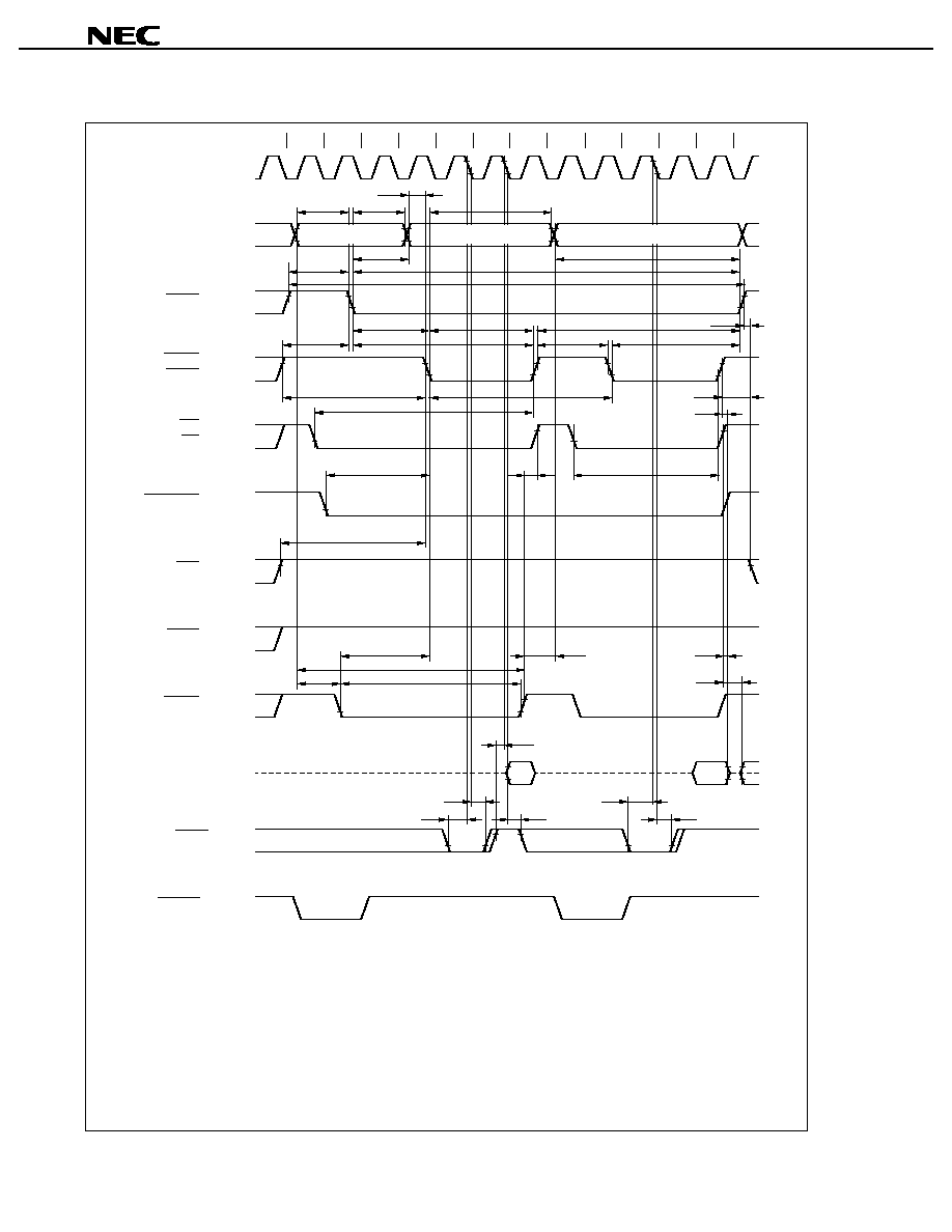
Preliminary Data Sheet U15390EJ1V0DS
54
µ
µ
µ
µ
PD703130
(g) DMA flyby transfer timing (DRAM (EDO, high-speed page)
external I/O transfer) (3/3)
TRPW
T1
TRHW
T2
TDAW
TW
T3
TCPW
TO1
TO2
TW
TDAW
<56>
<57>
<58>
<59>
<76>
<61>
<60>
<94>
<64>
<77>
<65>
<83>
<63>
<81>
<67>
<66>
<71>
<82>
<96>
<105>
<68>
<69>
<70>
<79>
<48>
<97>
<106>
<42>
<41>
<50>
<43>
<78>
<37>
<24>
<25>
<24>
<25>
<25>
<24>
Data
Data
CLKOUT (Output)
A0 to A23 (Output)
RASn (Output)
UCAS (Output)
LCAS (Output)
RD (Output)
OE (Output)
DMAAKm (Output)
WE (Output)
IORD (Output)
IOWR (Output)
D0 to D15 (I/O)
WAIT (Input)
BCYST (Output)
Row address
Column address
Column address
Remarks 1. This is the timing for the following case (n = 0 to 3, xx = 00 to 03, 10 to 13).
Number of waits due to the RPCxx bit of the DRCn register (TRPW): 1
Number of waits due to the RHCxx bit of the DRCn register (TRHW): 1
Number of waits due to the DACxx bit of the DRCn register (TDAW): 1
Number of waits due to the CPCxx bit of the DRCn register (TCPW): 1
Number of waits that are inserted for a source-side access during a DMA flyby transfer: 0
2. The broken lines indicate high impedance.
3. n = 3 to 5, m = 0 to 3
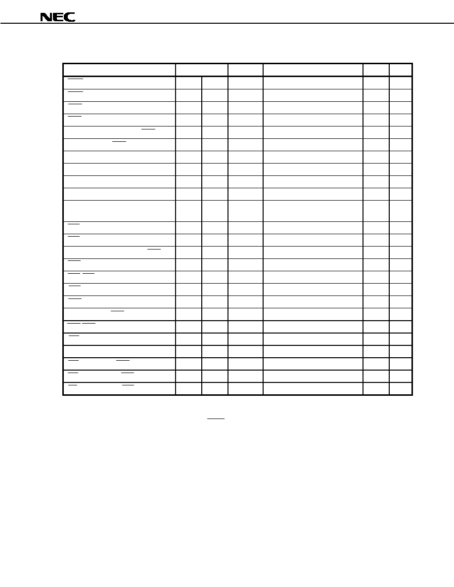
Preliminary Data Sheet U15390EJ1V0DS
55
µ
µ
µ
µ
PD703130
(h) DMA flyby transfer timing (external I/O
DRAM (EDO, high-speed page) transfer) (1/3)
Parameter
Symbol
Condition
MIN.
MAX.
Unit
WAIT setup time (to CLKOUT
)
<24>
t
SWK
15
ns
WAIT hold time (from CLKOUT
)
<25>
t
HKW
2
ns
IORD low-level width
<32>
t
WRDL
(2 + w
RH
+ w
DA
+ w
F
+ w)T ≠ 10
ns
IORD high-level width
<33>
t
WRDH
T ≠ 10
ns
Delay time from address to IORD
<34>
t
DARD
0.5T ≠ 10
ns
Delay time from IORD
to address
<35>
t
DRDA
(0.5 + i)T ≠ 10
ns
Row address setup time
<56>
t
ASR
(0.5 + w
RP
)T ≠ 10
ns
Row address hold time
<57>
t
RAH
(0.5 + w
RH
)T ≠ 10
ns
Column address setup time
<58>
t
ASC
0.5T ≠ 10
ns
Column address hold time
<59>
t
CAH
(1.5 + w
DA
+ w
F
)T ≠ 10
ns
Read/write cycle time
<60>
t
RC
(3 + w
RP
+ w
RH
+ w
DA
+ w
F
+ w)T
≠ 10
ns
RAS precharge time
<61>
t
RP
(0.5 + w
RP
)T ≠ 10
ns
RAS hold time
<63>
t
RSH
(1.5 + w
DA
+ w
F
)T ≠ 10
ns
Column address read time for RAS
<64>
t
RAL
(2 + w
CP
+ w
DA
+ w
F
+ w)T ≠ 10
ns
CAS pulse width
<65>
t
CAS
(1 + w
DA
+ w
F
)T ≠ 10
ns
CAS-RAS precharge time
<66>
t
CRP
(1 + w
RP
)T ≠ 10
ns
CAS hold time
<67>
t
CSH
(2 + w
RH
+ w
DA
+ w
F
+ w)T ≠ 10
ns
CAS precharge time
<71>
t
CPN
(2 + w
RP
+ w
RH
+ w)T ≠ 10
ns
Delay time from RAS to column address
<76>
t
RAD
(0.5 + w
RH
)T ≠ 10
ns
RAS-CAS delay time
<77>
t
RCD
(1 + w
RH
+ w)T ≠ 10
ns
CAS precharge time
<81>
t
CP
(0.5 + w
CP
+ w)T ≠ 10
ns
High-speed page mode cycle time
<82>
t
PC
(2 + w
CP
+ w
DA
+ w
F
+ w)T ≠ 10
ns
RAS hold time for CAS precharge
<83>
t
RHCP
(2.5 + w
CP
+ w
DA
+ w)T ≠ 10
ns
WE hold time (from CAS
)
<85>
t
WCH
(1 + w
DA
)T ≠ 10
ns
WE read time (from RAS
)
<88>
t
RWL
w
CP
= 0
(1.5 + w
DA
+ w)T ≠ 10
ns
Remarks 1. T = t
CYK
2. w: The number of waits due to WAIT.
3. w
RH
: The number of waits due to the RHCxx bit of the DRCn register (n = 0 to 3, xx = 00 to 03, 10 to
13).
4. w
DA
: The number of waits due to the DACxx bit of the DRCn register (n = 0 to 3, xx = 00 to 03, 10 to
13).
5. w
RP
: The number of waits due to the RPCxx bit of the DRCn register (n = 0 to 3, xx = 00 to 03, 10 to
13).
6. w
CP
: The number of waits due to the CPCxx bit of the DRCn register (n = 0 to 3, xx = 00 to 03, 10 to
13).
7. w
F
: The number of waits that are inserted for a source-side access during a DMA flyby transfer.
8. i: The number of idle states that are inserted when a write cycle follows a read cycle.
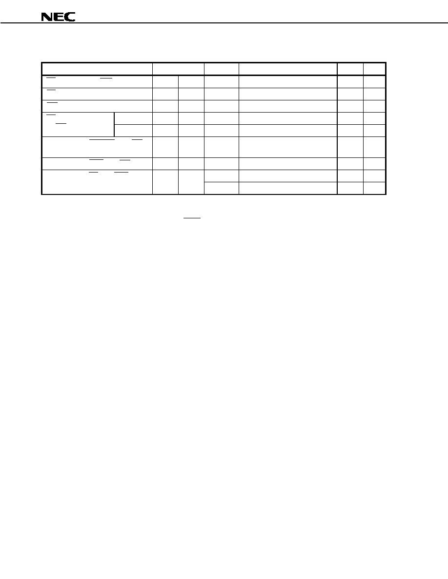
Preliminary Data Sheet U15390EJ1V0DS
56
µ
µ
µ
µ
PD703130
(h) DMA flyby transfer timing (external I/O
DRAM (EDO, high-speed page) transfer) (2/3)
Parameter
Symbol
Condition
MIN.
MAX.
Unit
WE read time (from CAS
)
<89>
t
CWL
w
CP
= 0
(1 + w
DA
+ w)T ≠ 10
ns
WE pulse width
<92>
t
WP
w
CP
= 0
(1 + w
DA
+ w)T ≠ 10
ns
RAS pulse width
<94>
t
RASP
(2.5 + w
RH
+ w
DA
+ w
F
+ w)T ≠ 10
ns
Off-page
<101>
t
WCS1
w
CP
= 0
(1 + w
RH
+ w
RP
+ w)T ≠ 10
ns
WE setup time
(to CAS
)
On-page
<102>
t
WCS2
w
CP
1
w
CP
T ≠ 10
ns
Delay time from DMAAKm
to CAS
<105>
t
DDACS
(1.5 + w
RH
+ w)T ≠ 10
ns
Delay time from IORD
to CAS
<106>
t
DRDCS
(1 + w
RH
+ w)T ≠ 10
ns
Delay time from WE
to IORD
<107>
t
DWERD
w
F
= 0
0
ns
w
F
= 1
T ≠ 10
ns
Remarks 1. T = t
CYK
2. w: The number of waits due to WAIT.
3. w
RH
: The number of waits due to the RHCxx bit of the DRCn register (n = 0 to 3, xx = 00 to 03, 10 to
13).
4. w
DA
: The number of waits due to the DACxx bit of the DRCn register (n = 0 to 3, xx = 00 to 03, 10 to
13).
5. w
RP
: The number of waits due to the RPCxx bit of the DRCn register (n = 0 to 3, xx = 00 to 03, 10 to
13).
6. w
CP
: The number of waits due to the CPCxx bit of the DRCn register (n = 0 to 3, xx = 00 to 03, 10 to
13).
7. w
F
: The number of waits that are inserted for a source-side access during a DMA flyby transfer.
8. m = 0 to 3
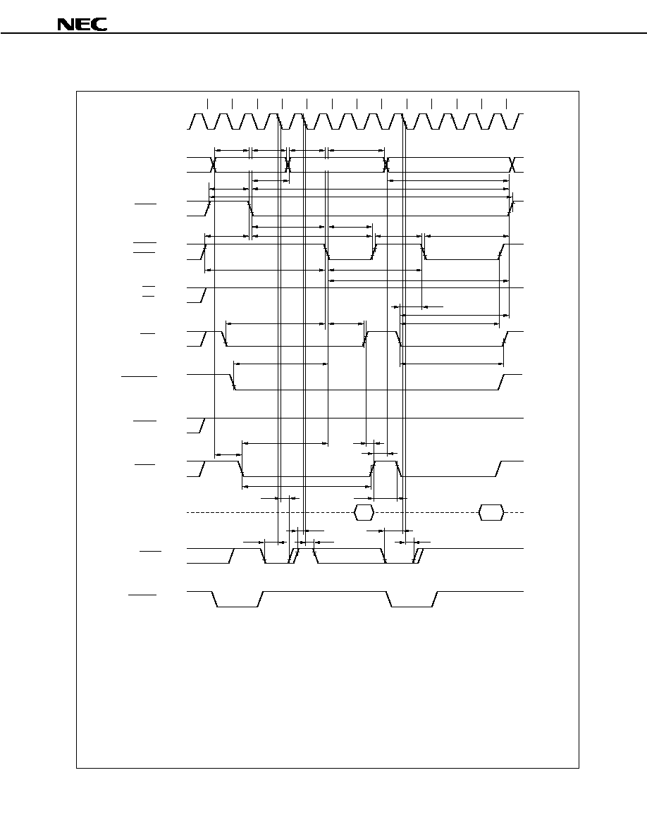
Preliminary Data Sheet U15390EJ1V0DS
57
µ
µ
µ
µ
PD703130
(h) DMA flyby transfer timing (external I/O
DRAM (EDO, high-speed page) transfer) (3/3)
Remarks 1. This is the timing for the following case (n = 0 to 3, xx = 00 to 03, 10 to 13).
Number of waits due to the RPCxx bit of the DRCn register (TRPW): 1
Number of waits due to the RHCxx bit of the DRCn register (TRHW): 1
Number of waits due to the DACxx bit of the DRCn register (TDAW): 1
Number of waits due to the CPCxx bit of the DRCn register (TCPW): 1
Number of waits that are inserted for a source-side access during a DMA flyby transfer: 0
2. The broken lines indicate high impedance.
3. n = 3 to 5, m = 0 to 3
TRPW
T1
TRHW
TW
T2
TDAW
T3
TCPW
TW
TO2
TDAW
TO1
<56>
<57>
<58>
<76>
<61>
<60>
<94>
<64>
<77>
<65>
<63>
<81>
<67>
<66>
<71>
<82>
<101>
<105>
<83>
<85>
<89>
<106>
<34>
<107>
<33>
<24>
<25>
<24>
<25>
<24>
Data
Data
<59>
<88>
<102>
<92>
<35>
<32>
<25>
CLKOUT (Output)
A0 to A23 (Output)
RASn (Output)
UCAS (Output)
LCAS (Output)
RD (Output)
OE (Output)
DMAAKm (Output)
WE (Output)
IOWR (Output)
IORD (Output)
D0 to D15 (I/O)
WAIT (Input)
BCYST (Output)
Row address
Column address
Column address
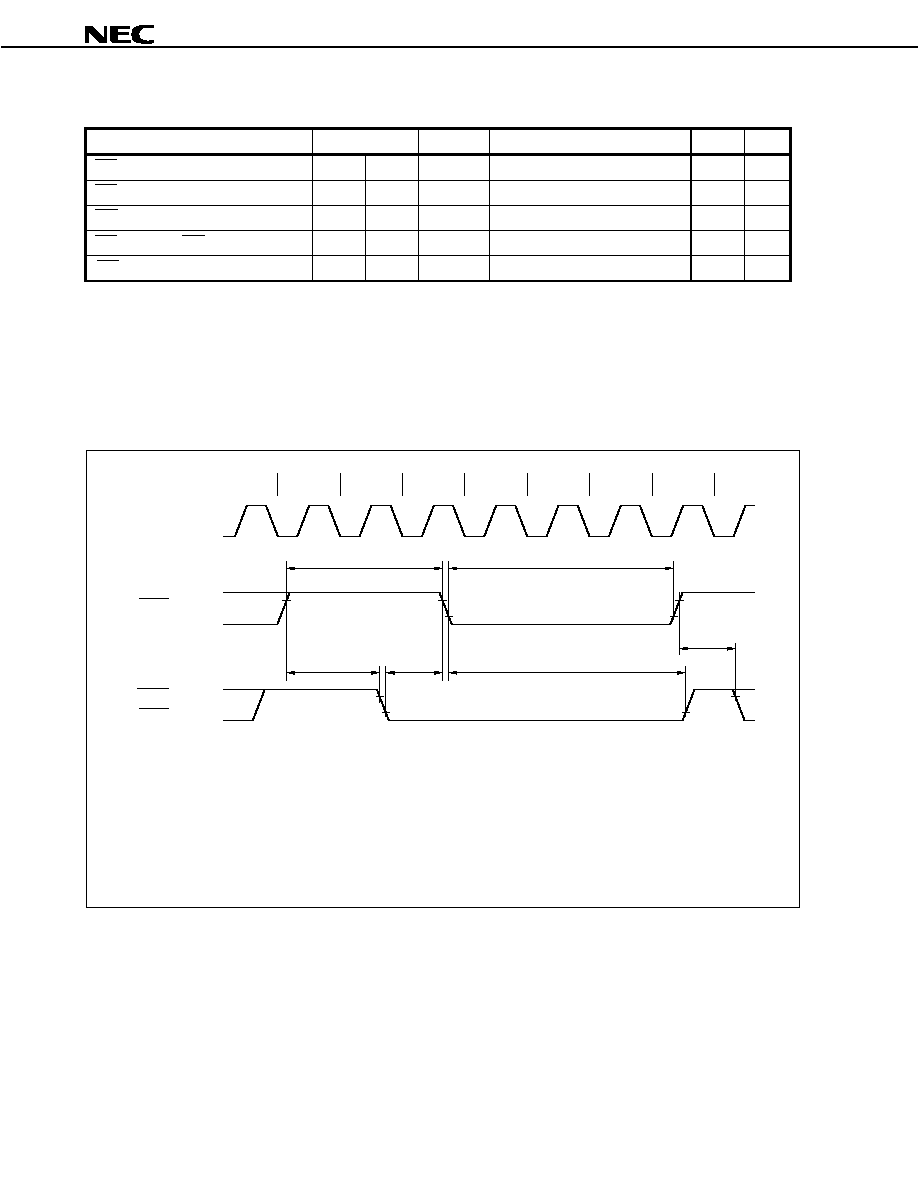
Preliminary Data Sheet U15390EJ1V0DS
58
µ
µ
µ
µ
PD703130
(i) CBR refresh timing
Parameter
Symbol
Condition
MIN.
MAX.
Unit
RAS precharge time
<61>
t
RP
(1.5 + w
RRW
)T ≠ 10
ns
RAS pulse width
<62>
t
RAS
(1.5 + w
RCW
Note
)T ≠ 10
ns
CAS hold time
<108>
t
CHR
(1.5 + w
RCW
Note
)T ≠ 10
ns
RAS precharge CAS hold time
<110>
t
RPC
(0.5 + w
RRW
)T ≠ 10
ns
CAS setup time
<113>
t
CSR
T ≠ 10
ns
Note At least one clock cycle is inserted by default for w
RCW
regardless of the settings of the RCW0 to RCW2
bits of the RWC register.
Remarks 1. T = t
CYK
2. w
RRW
: The number of waits due to the RRW0 and RRW1 bits of the RWC register.
3. w
RCW
: The number of waits due to the RCW0 to RCW2 bits of the RWC register.
Note This TRCW is always inserted regardless of the settings of the RCW0 to RCW2 bits of the RWC register.
Remarks 1. This is the timing for the following case.
Number of waits due to the RRW0 and RRW1 bits of the RWC register (TRRW): 1
Number of waits due to the RCW0 to RCW2 bits of the RWC register (TRCW): 2
2. n = 3 to 5
TI
T3
TRCW
TRCW
Note
T2
T1
TRRW
RASn (Output)
<62>
UCAS (Output)
<108>
<110>
<61>
<113>
<110>
LCAS (Output)
CLKOUT (Output)
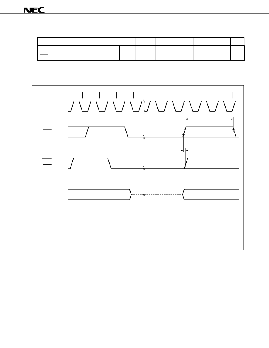
Preliminary Data Sheet U15390EJ1V0DS
59
µ
µ
µ
µ
PD703130
(j) CBR self-refresh timing
Parameter
Symbol
Condition
MIN.
MAX.
Unit
CAS hold time
<114>
t
CHS
-5
ns
RAS precharge time
<115>
t
RPS
(1 + 2w
SRW
)T ≠ 10
ns
Remarks 1. T = t
CYK
2. w
SRW
: The number of waits due to the SRW0 to SRW2 bits of the RWC register.
Remarks 1. This is the timing for the following case.
Number of waits due to the RRW0 and RRW1 bits of the RWC register (TRRW): 1
Number of waits due to the RCW0 to RCW2 bits of the RWC register (TRCW): 1
Number of waits due to the SRW0 to SRW2 bits of the RWC register (TSRW): 2
2. The broken lines indicate high impedance.
3. n = 3 to 5
TH
TH
TH
TRRW
TSRW
TI
TH
TRCW
TSRW
Output signals
other than above
<115>
<114>
CLKOUT (Output)
RASn (Output)
UCAS (Output)
LCAS (Output)
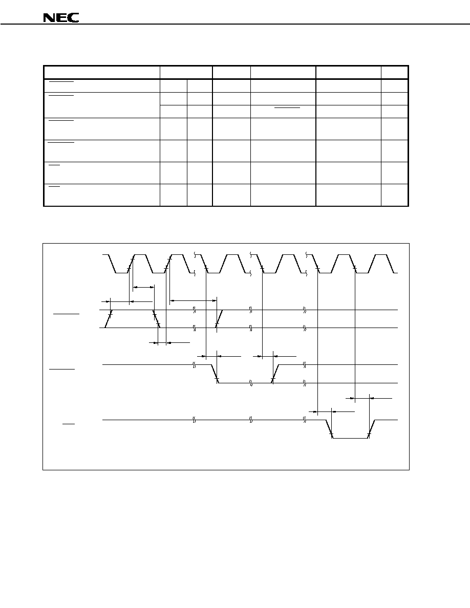
Preliminary Data Sheet U15390EJ1V0DS
60
µ
µ
µ
µ
PD703130
(7) DMAC timing
Parameter
Symbol
Condition
MIN.
MAX.
Unit
DMARQn setup time (to CLKOUT
)
<116>
t
SDRK
15
ns
<117>
t
HKDR1
2
ns
DMARQn hold time (from CLKOUT
)
<118>
t
HKDR2
Until DMAAKn
ns
DMAAKn output delay time
(from CLKOUT
)
<119>
t
DKDA
2
10
ns
DMAAKn output hold time
(from CLKOUT
)
<120>
t
HKDA
2
10
ns
TCn output delay time
(from CLKOUT
)
<121>
t
DKTC
2
10
ns
TCn output hold time
(from CLKOUT
)
<122>
t
HKTC
2
10
ns
Remark n = 0 to 3
Remark n = 0 to 3
<121>
DMARQn (Input)
DMAAKn (Output)
TCn (Output)
<122>
<120>
<119>
<118>
<117>
<116>
<116>
CLKOUT (Output)

Preliminary Data Sheet U15390EJ1V0DS
61
µ
µ
µ
µ
PD703130
[MEMO]
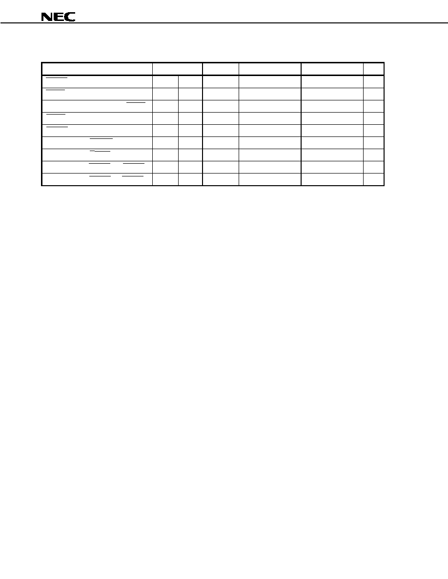
Preliminary Data Sheet U15390EJ1V0DS
62
µ
µ
µ
µ
PD703130
(8) Bus hold timing (1/2)
Parameter
Symbol
Condition
MIN.
MAX.
Unit
HLDRQ setup time (to CLKOUT
)
<123>
t
SHRK
15
ns
HLDRQ hold time (from CLKOUT
)
<124>
t
HKHR
2
ns
Delay time from CLKOUT
to HLDAK
<125>
t
DKHA
2
10
ns
HLDRQ high-level width
<126>
t
WHQH
T + 17
ns
HLDAK low-level width
<127>
t
WHAL
T ≠ 8
ns
Delay time from CLKOUT
to bus float
<128>
t
DKCF
10
ns
Delay time from HLDAK
to bus output <129>
t
DHAC
0
ns
Delay time from HLDRQ
to HLDAK
<130>
t
DHQHA1
2.5T
ns
Delay time from HLDRQ
to HLDAK
<131>
t
DHQHA2
0.5T
1.5T
ns
Remark T = t
CYK
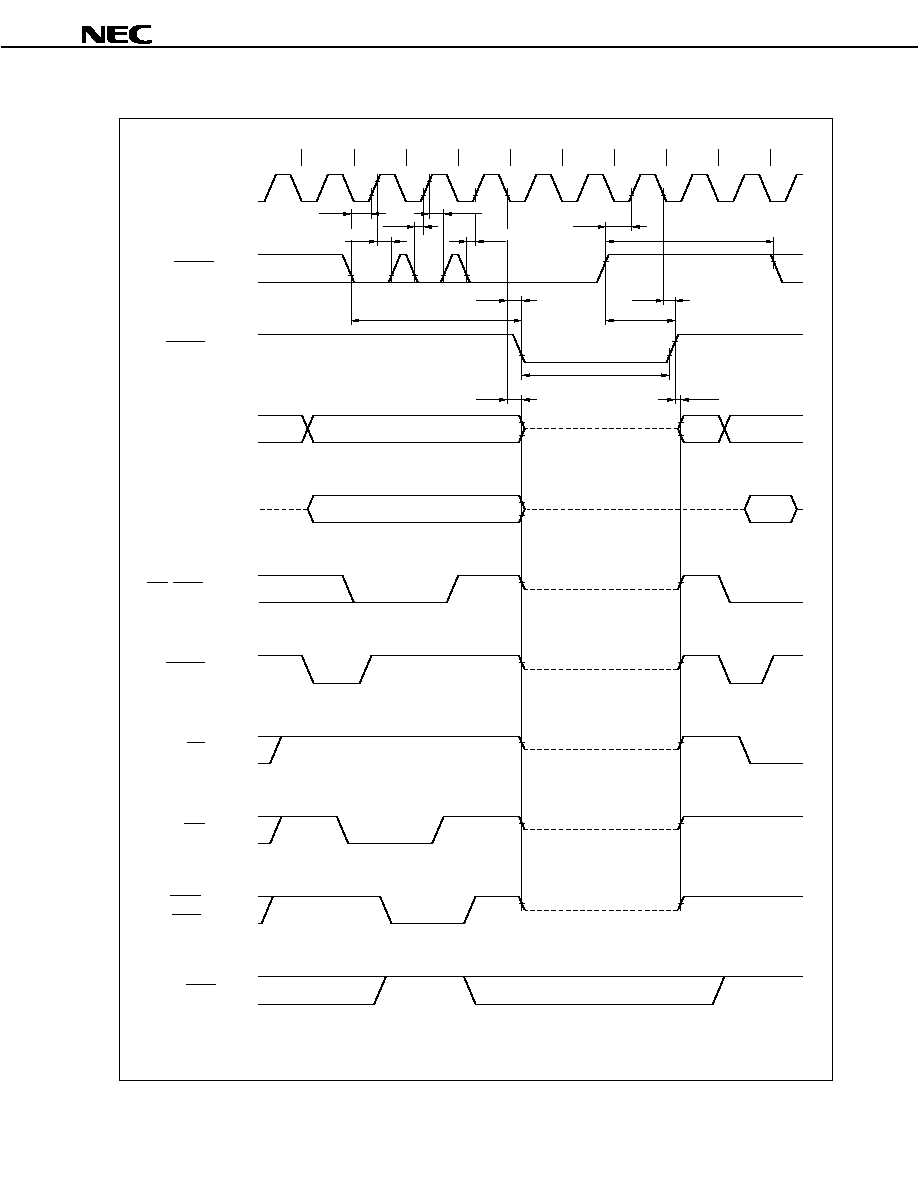
Preliminary Data Sheet U15390EJ1V0DS
63
µ
µ
µ
µ
PD703130
(8) Bus hold timing (2/2)
T1
T2
T3
TI
TH
TH
TH
TI
T1
A0
to A23 (Output)
D0
to D15 (I/O)
<123>
<124>
<124>
<123>
<123>
<123>
<126>
<130>
<125>
<127>
<125>
<128>
<129>
<131>
Address
Undefined
Data
CLKOUT (Output)
HLDRQ (Input)
HLDAK (Output)
CSn/RASm (Output)
BCYST (Output)
RD (Output)
WE (Output)
WAIT (Input)
UCAS (Output)
LCAS (Output)
Remarks 1. The broken lines indicate high impedance.
2. n = 0, 3 to 5, m = 3 to 5
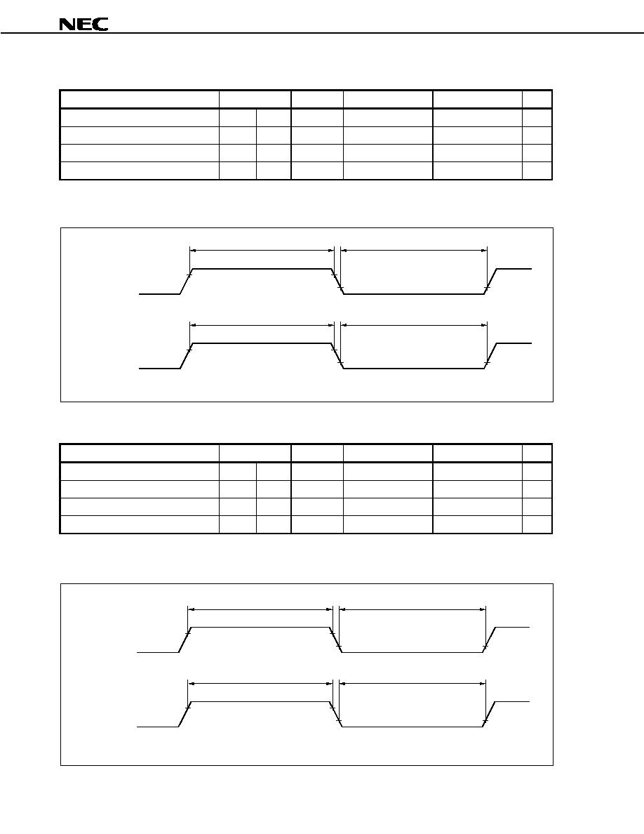
Preliminary Data Sheet U15390EJ1V0DS
64
µ
µ
µ
µ
PD703130
(9) Interrupt timing
Parameter
Symbol
Condition
MIN.
MAX.
Unit
NMI high-level width
<132>
t
WNIH
500
ns
NMI low-level width
<133>
t
WNIL
500
ns
INTPn high-level width
<134>
t
WITH
4T + 10
ns
INTPn low-level width
<135>
t
WITL
4T + 10
ns
Remarks 1. n = 100 to 103, 110 to 113, 130
2. T = t
CYK
NMI (Input)
<132>
<133>
INTPn (Input)
<134>
<135>
Remark n = 100 to 103, 110 to 113, 130
(10) RPU timing
Parameter
Symbol
Condition
MIN.
MAX.
Unit
TI13 high-level width
<136>
t
WTIH
3T + 18
ns
TI13 low-level width
<137>
t
WTIL
3T + 18
ns
TCLR1n high-level width
<138>
t
WTCH
3T + 18
ns
TCLR1n low-level width
<139>
t
WTCL
3T + 18
ns
Remarks 1. n = 0 to 2
2. T = t
CYK
Remark n = 0 to 2
TI13 (Input)
<136>
<137>
TCLR1n (Input)
<138>
<139>
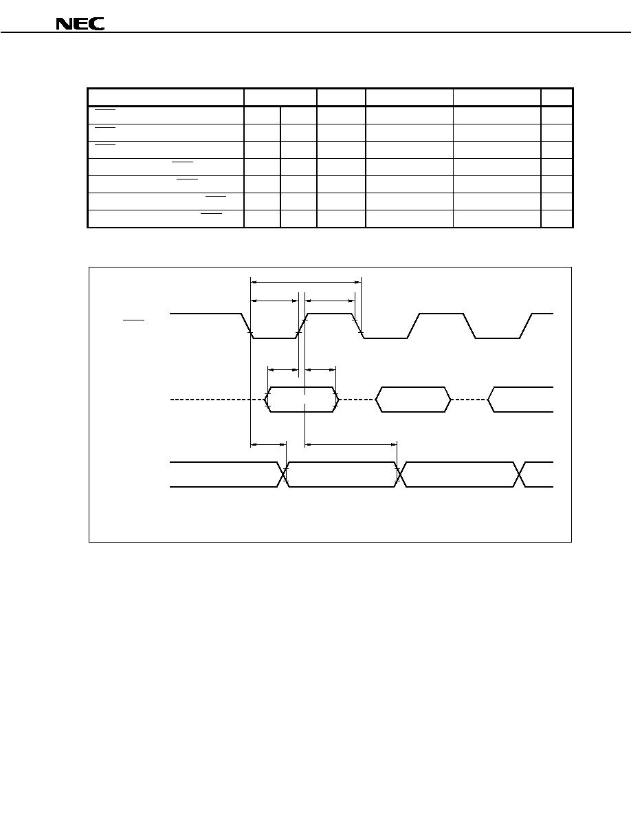
Preliminary Data Sheet U15390EJ1V0DS
65
µ
µ
µ
µ
PD703130
(11) UART0, UART1 timing (clock-synchronized or master mode only)
Parameter
Symbol
Condition
MIN.
MAX.
Unit
SCKn cycle
<140>
t
CYSK0
Output
250
ns
SCKn high-level width
<141>
t
WSK0H
Output
0.5t
CYSK0
≠ 20
ns
SCKn low-level width
<142>
t
WSK0L
Output
0.5t
CYSK0
≠ 20
ns
RXDn setup time (to SCKn
)
<143>
t
SRXSK
30
ns
RXDn hold time (from SCKn
)
<144>
t
HSKRX
0
ns
TXDn output delay time (from SCKn
)
<145>
t
DSKTX
20
ns
TXDn output hold time (from SCKn
)
<146>
t
HSKTX
0.5t
CYSK0
≠ 5
ns
Remark n = 0, 1
SCKn (I/O)
<142>
<140>
<141>
RXDn (Input)
<143>
<144>
Input data
TXDn (Output)
<145>
Output data
<146>
Remarks 1. The broken lines indicate high impedance.
2. n = 0, 1
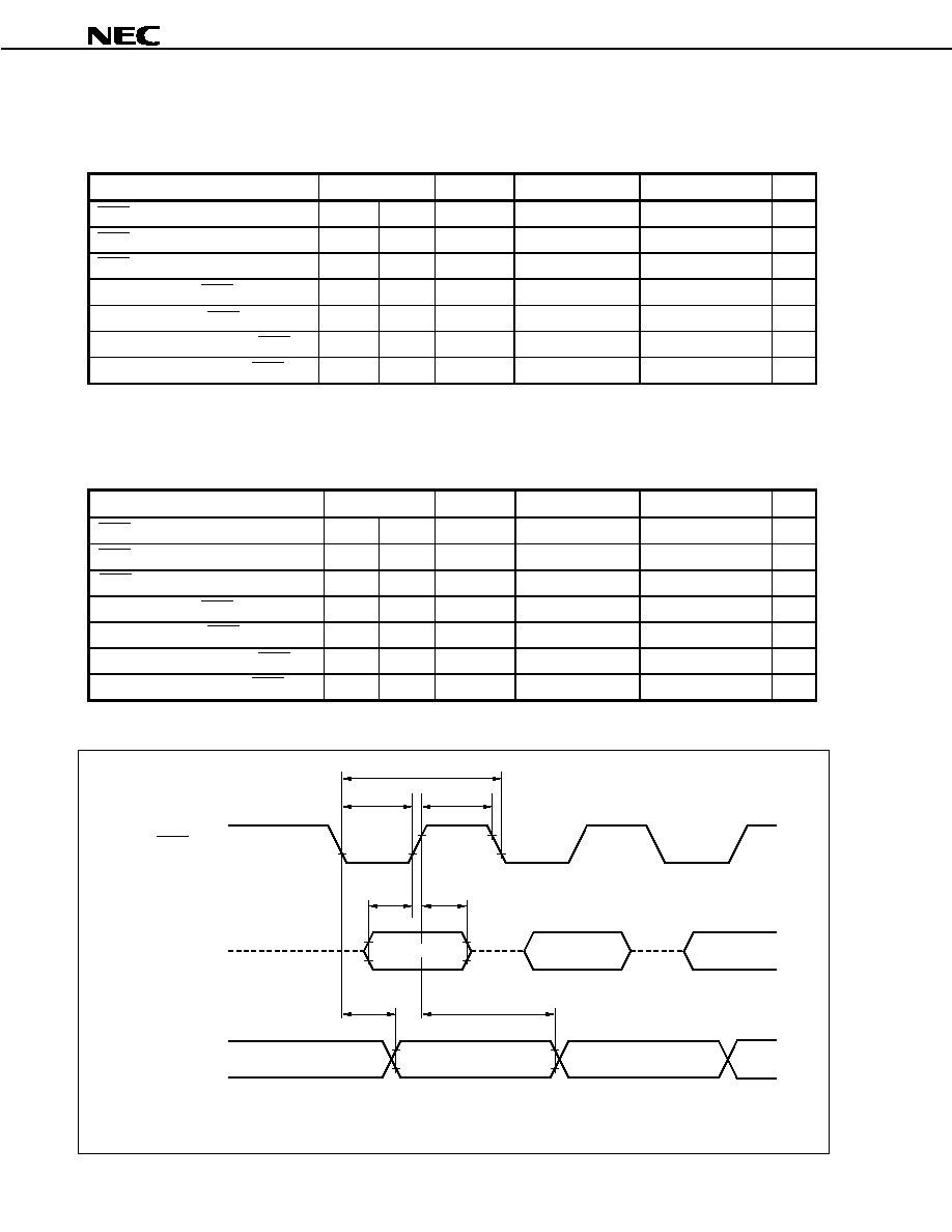
Preliminary Data Sheet U15390EJ1V0DS
66
µ
µ
µ
µ
PD703130
(12) CSI0, CSI1 timing
(a) Master mode
Parameter
Symbol
Condition
MIN.
MAX.
Unit
SCKn cycle
<147>
t
CYSK1
Output
100
ns
SCKn high-level width
<148>
t
WSK1H
Output
0.5t
CYSK1
≠ 20
ns
SCKn low-level width
<149>
t
WSK1L
Output
0.5t
CYSK1
≠ 20
ns
SIn setup time (to SCKn
)
<150>
t
SSISK
30
ns
SIn hold time (from SCKn
)
<151>
t
HSKSI
0
ns
SOn output delay time (from SCKn
)
<152>
t
DSKSO
20
ns
SOn output hold time (from SCKn
)
<153>
t
HSKSO
0.5t
CYSK1
≠ 5
ns
Remark n = 0, 1
(b) Slave mode
Parameter
Symbol
Condition
MIN.
MAX.
Unit
SCKn cycle
<147>
t
CYSK1
Input
100
ns
SCKn high-level width
<148>
t
WSK1H
Input
30
ns
SCKn low-level width
<149>
t
WSK1L
Input
30
ns
SIn setup time (to SCKn
)
<150>
t
SSISK
10
ns
SIn hold time (from SCKn
)
<151>
t
HSKSI
10
ns
SOn output delay time (from SCKn
)
<152>
t
DSKSO
30
ns
SOn output hold time (from SCKn
)
<153>
t
HSKSO
t
WSK1H
ns
Remark n = 0, 1
SCKn (I/O)
<149>
<147>
<148>
Sln (Input)
<150>
<151>
Input data
SOn (Output)
<152>
Output data
<153>
Remarks 1. The broken lines indicate high impedance.
2. n = 0, 1
Preliminary Data Sheet U15390EJ1V0DS
67
µ
µ
µ
µ
PD703130
A/D Converter Characteristics (T
A
= ≠40 to +85
∞
∞
∞
∞C, V
DD
= CV
DD
= 3.0 to 3.6 V, HV
DD
= 5.0 V
±
±
±
±10%, V
SS
= 0 V,
HV
DD
≠ 0.5 V
AV
DD
HV
DD
, output pin load capacitance: C
L
= 50 pF)
Parameter
Symbol
Condition
MIN.
TYP.
MAX.
Unit
Resolution
≠
10
bit
Overall error
≠
±4
LSB
Quantization error
≠
±1/2
LSB
Conversion time
t
CONV
5
10
µs
Sampling time
t
SAMP
Conversion
clock
Note
/6
ns
Zero scale error
≠
±4
LSB
Scale error
≠
±4
LSB
Linearity error
≠
±3
LSB
Analog input voltage
V
IAN
-0.3
AV
REF
+ 0.3
V
Analog input resistance
R
AN
2
M
AV
REF
input voltage
AV
REF
AV
REF
= AV
DD
4.5
5.5
V
AV
REF
input current
AI
REF
2.0
mA
AV
DD
current
AI
DD
6
mA
Note Conversion clock is the number of clocks set by the ADM1 register.
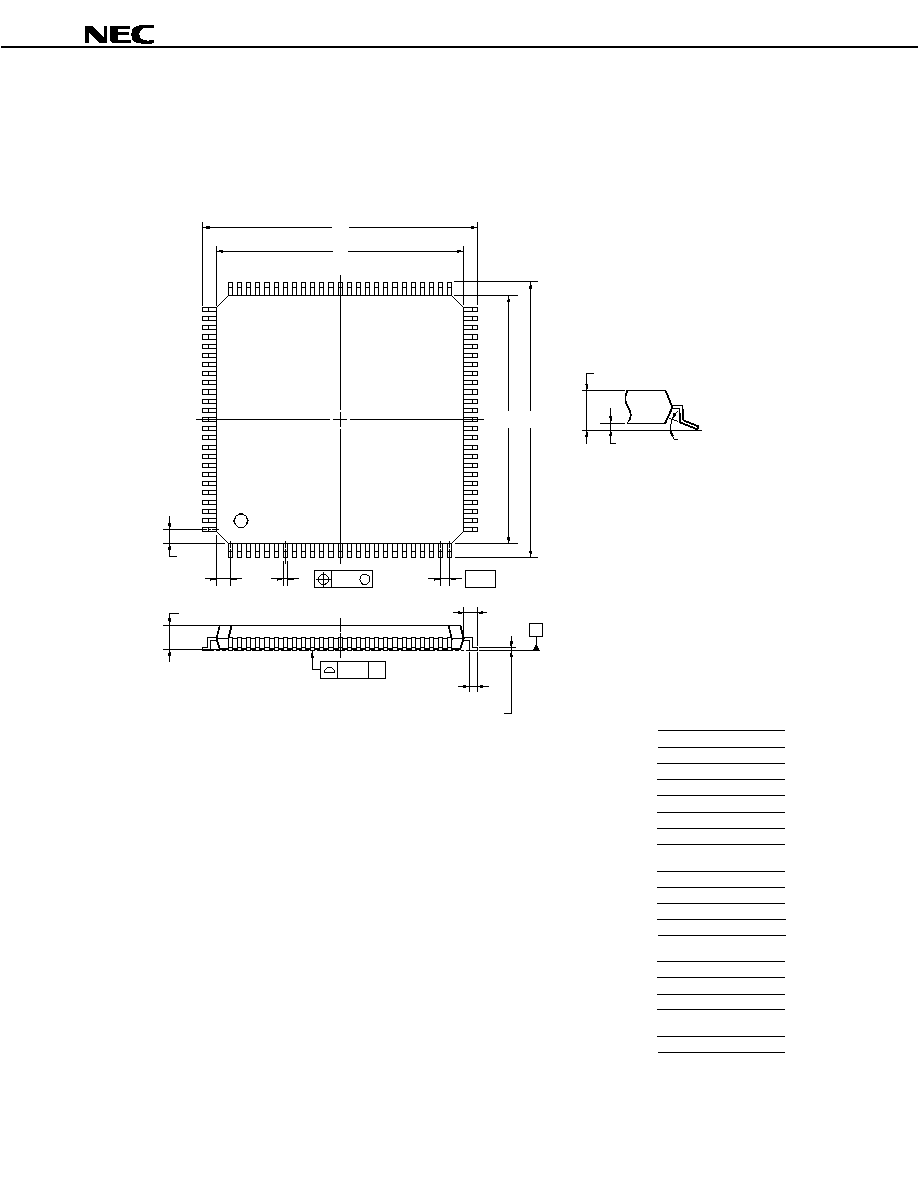
Preliminary Data Sheet U15390EJ1V0DS
68
µ
µ
µ
µ
PD703130
4. PACKAGE DRAWING
100-PIN PLASTIC LQFP (FINE PITCH) (14x14)
NOTE
Each lead centerline is located within 0.08 mm of
its true position (T.P.) at maximum material condition.
ITEM
MILLIMETERS
A
B
D
G
16.00
±
0.20
14.00
±
0.20
0.50 (T.P.)
1.00
J
16.00
±
0.20
K
C
14.00
±
0.20
I
0.08
1.00
±
0.20
L
0.50
±
0.20
F
1.00
N
P
Q
0.08
1.40
±
0.05
0.10
±
0.05
S100GC-50-8EU, 8EA-2
S
1.60 MAX.
H
0.22
+
0.05
-
0.04
M
0.17
+
0.03
-
0.07
R
3
∞+
7
∞
-
3
∞
1
25
26
50
100
76
75
51
S
S
N
J
detail of lead end
C
D
A
B
R
K
M
L
P
I
S
Q
G
F
M
H

Preliminary Data Sheet U15390EJ1V0DS
69
µ
µ
µ
µ
PD703130
5. RECOMMENDED SOLDERING CONDITIONS
TBD
Preliminary Data Sheet U15390EJ1V0DS
70
µ
µ
µ
µ
PD703130
NOTES FOR CMOS DEVICES
1
PRECAUTION AGAINST ESD FOR SEMICONDUCTORS
Note:
Strong electric field, when exposed to a MOS device, can cause destruction of the gate oxide and
ultimately degrade the device operation. Steps must be taken to stop generation of static electricity
as much as possible, and quickly dissipate it once, when it has occurred. Environmental control
must be adequate. When it is dry, humidifier should be used. It is recommended to avoid using
insulators that easily build static electricity. Semiconductor devices must be stored and transported
in an anti-static container, static shielding bag or conductive material. All test and measurement
tools including work bench and floor should be grounded. The operator should be grounded using
wrist strap. Semiconductor devices must not be touched with bare hands. Similar precautions need
to be taken for PW boards with semiconductor devices on it.
2
HANDLING OF UNUSED INPUT PINS FOR CMOS
Note:
No connection for CMOS device inputs can be cause of malfunction. If no connection is provided
to the input pins, it is possible that an internal input level may be generated due to noise, etc., hence
causing malfunction. CMOS devices behave differently than Bipolar or NMOS devices. Input levels
of CMOS devices must be fixed high or low by using a pull-up or pull-down circuitry. Each unused
pin should be connected to V
DD
or GND with a resistor, if it is considered to have a possibility of
being an output pin. All handling related to the unused pins must be judged device by device and
related specifications governing the devices.
3
STATUS BEFORE INITIALIZATION OF MOS DEVICES
Note:
Power-on does not necessarily define initial status of MOS device. Production process of MOS
does not define the initial operation status of the device. Immediately after the power source is
turned ON, the devices with reset function have not yet been initialized. Hence, power-on does
not guarantee out-pin levels, I/O settings or contents of registers. Device is not initialized until the
reset signal is received. Reset operation must be executed immediately after power-on for devices
having reset function.
Reference materials
Electrical Characteristics for Microcomputer (U15170J
Note
)
Note This document number is that of Japanese version.
The related documents indicated in this publication may include preliminary versions. However, preliminary
versions are not marked as such.
V850E/MS1, V850E/MS2, and V850 Family are trademarks of NEC Corporation.

Preliminary Data Sheet U15390EJ1V0DS
71
µ
µ
µ
µ
PD703130
Regional Information
Some information contained in this document may vary from country to country. Before using any NEC
product in your application, pIease contact the NEC office in your country to obtain a list of authorized
representatives and distributors. They will verify:
∑
Device availability
∑
Ordering information
∑
Product release schedule
∑
Availability of related technical literature
∑
Development environment specifications (for example, specifications for third-party tools and
components, host computers, power plugs, AC supply voltages, and so forth)
∑
Network requirements
In addition, trademarks, registered trademarks, export restrictions, and other legal issues may also vary
from country to country.
NEC Electronics Inc. (U.S.)
Santa Clara, California
Tel: 408-588-6000
800-366-9782
Fax: 408-588-6130
800-729-9288
NEC Electronics (Germany) GmbH
Duesseldorf, Germany
Tel: 0211-65 03 02
Fax: 0211-65 03 490
NEC Electronics (UK) Ltd.
Milton Keynes, UK
Tel: 01908-691-133
Fax: 01908-670-290
NEC Electronics Italiana s.r.l.
Milano, Italy
Tel: 02-66 75 41
Fax: 02-66 75 42 99
NEC Electronics (Germany) GmbH
Benelux Office
Eindhoven, The Netherlands
Tel: 040-2445845
Fax: 040-2444580
NEC Electronics (France) S.A.
Velizy-Villacoublay, France
Tel: 01-3067-5800
Fax: 01-3067-5899
NEC Electronics (France) S.A.
Madrid Office
Madrid, Spain
Tel: 091-504-2787
Fax: 091-504-2860
NEC Electronics (Germany) GmbH
Scandinavia Office
Taeby, Sweden
Tel: 08-63 80 820
Fax: 08-63 80 388
NEC Electronics Hong Kong Ltd.
Hong Kong
Tel: 2886-9318
Fax: 2886-9022/9044
NEC Electronics Hong Kong Ltd.
Seoul Branch
Seoul, Korea
Tel: 02-528-0303
Fax: 02-528-4411
NEC Electronics Singapore Pte. Ltd.
Novena Square, Singapore
Tel: 253-8311
Fax: 250-3583
NEC Electronics Taiwan Ltd.
Taipei, Taiwan
Tel: 02-2719-2377
Fax: 02-2719-5951
NEC do Brasil S.A.
Electron Devices Division
Guarulhos-SP, Brasil
Tel: 11-6462-6810
Fax: 11-6462-6829
J01.2

µ
µ
µ
µ
PD703130
∑
The information contained in this document is being issued in advance of the production cycle for the
device. The parameters for the device may change before final production or NEC Corporation, at its own
discretion, may withdraw the device prior to its production.
∑
No part of this document may be copied or reproduced in any form or by any means without the prior written
consent of NEC Corporation. NEC Corporation assumes no responsibility for any errors which may appear in
this document.
∑
NEC Corporation does not assume any liability for infringement of patents, copyrights or other intellectual property
rights of third parties by or arising from use of a device described herein or any other liability arising from use
of such device. No license, either express, implied or otherwise, is granted under any patents, copyrights or other
intellectual property rights of NEC Corporation or others.
∑
Descriptions of circuits, software, and other related information in this document are provided for illustrative
purposes in semiconductor product operation and application examples. The incorporation of these circuits,
software, and information in the design of the customer's equipment shall be done under the full responsibility
of the customer. NEC Corporation assumes no responsibility for any losses incurred by the customer or third
parties arising from the use of these circuits, software, and information.
∑
While NEC Corporation has been making continuous effort to enhance the reliability of its semiconductor devices,
the possibility of defects cannot be eliminated entirely. To minimize risks of damage or injury to persons or
property arising from a defect in an NEC semiconductor device, customers must incorporate sufficient safety
measures in its design, such as redundancy, fire-containment, and anti-failure features.
∑
NEC devices are classified into the following three quality grades:
"Standard", "Special", and "Specific". The Specific quality grade applies only to devices developed based on a
customer designated "quality assurance program" for a specific application. The recommended applications of
a device depend on its quality grade, as indicated below. Customers must check the quality grade of each device
before using it in a particular application.
Standard: Computers, office equipment, communications equipment, test and measurement equipment,
audio and visual equipment, home electronic appliances, machine tools, personal electronic
equipment and industrial robots
Special: Transportation equipment (automobiles, trains, ships, etc.), traffic control systems, anti-disaster
systems, anti-crime systems, safety equipment and medical equipment (not specifically designed
for life support)
Specific: Aircraft, aerospace equipment, submersible repeaters, nuclear reactor control systems, life
support systems or medical equipment for life support, etc.
The quality grade of NEC devices is "Standard" unless otherwise specified in NEC's Data Sheets or Data Books.
If customers intend to use NEC devices for applications other than those specified for Standard quality grade,
they should contact an NEC sales representative in advance.
M5 98. 8