 | –≠–ª–µ–∫—Ç—Ä–æ–Ω–Ω—ã–π –∫–æ–º–ø–æ–Ω–µ–Ω—Ç: CMOS-8LHD | –°–∫–∞—á–∞—Ç—å:  PDF PDF  ZIP ZIP |
April 1996
NEC Electronics Inc.
A10616EU1V0DS00
CMOS-8LHD
3.3-Volt, 0.5-Micron
CMOS Gate Arrays
Preliminary
Description
NEC's CMOS-8LHD gate-array family combines cell-
based-level densities with the fast time-to-market and low
development costs of gate arrays. With a unique
heterogeneous cell architecture, CMOS-8LHD provides
the very dense logic and RAM capabilities required to build
devices for fast computer and communications systems.
NEC delivers high-speed, 0.5-micron, drawn gate length
(Leff=0.35-micron), three-level metal, CMOS technology
with an extensive family of macros. I/O macros include
GTL, HSTL, and pECL. TTL CMOS I/Os are provided with
5-V tolerance for applications requiring interface to 5-V
logic. PCI signaling standards are also supported,
including 3.3-V, 66 MHz PCI. The technology is enhanced
by a set of advanced features, including phase-locked
loops, clock tree synthesis, and high-speed memory. The
CMOS-8LHD gate-array family of 3.3-V devices consists
of 12 masters, offered in densities of 75K raw gates to
1.123 million raw gates. Usable gates range from 45K to
674K used gates.
The gate-array family is supported by NEC's OpenCAD
Æ
design system, a mixture of popular third-party EDA tools,
and proprietary NEC tools. NEC proprietary tools include
the GALET floorplanner, which helps to reduce design
time and improve design speed, and a clock tree synthesis
tool that automatically builds a balanced-buffer clock tree
to minimize on-chip clock skew.
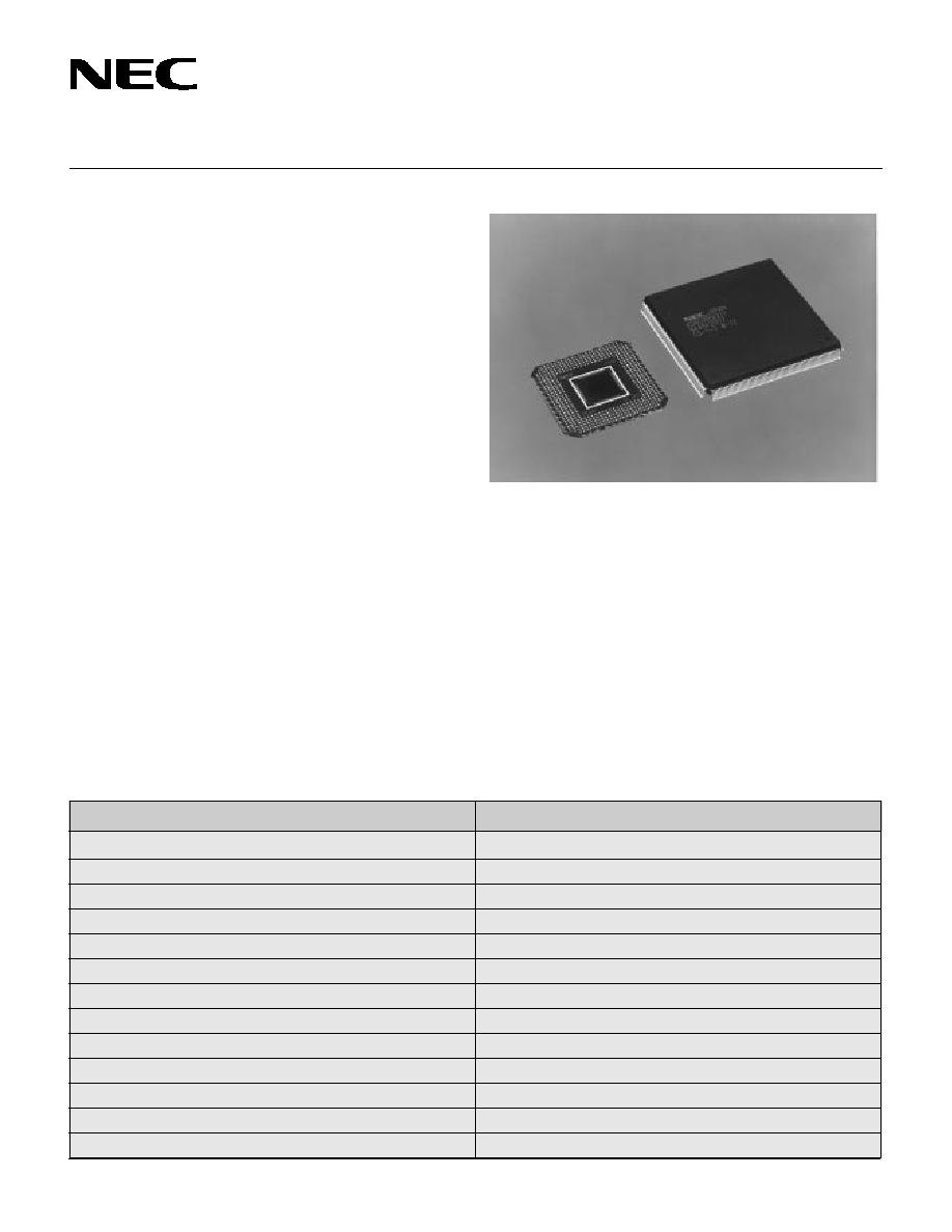
Figure 1. CMOS-8LHD Package Options: BGA & QFP
Table 1. CMOS-8LHD Family Features and Benefits
CMOS-8LHD Family Features
CMOS-8LHD Family Benefits
∑ 0.5-micron (drawn), 3-level metal CMOS technology
∑ Delivers very dense, cost-effective gate-array products
∑ 12 base arrays with raw gates from 75K to 1.123M
∑ Provides base sizes to give best fit in core-limited designs
∑ Optimized pad pitch for low-cost packaging
∑ Minimizes assembly cost for popular BGA and PQFPs
∑ Cell-Based Array (CBA) architecture
∑ Achieves cell-based logic densities, reducing core size
∑ High-density, high-speed RAM compiler
∑ Provides high-density RAM in fast gate-array design time
∑ PCI, GTL, and HSTL interface buffers
∑ Supports popular high-speed interface standards
∑ Full range of 5V-protected I/O drive strengths
∑ Allows interface with 5-V logic while protecting 3.3-V ASIC
∑ Phase-Locked Loop (PLL) macros in development
∑ Eliminates clock insertion delay; reduces total clock skew
∑ Low power dissipation: 0.21 µW/MHz/gate
∑ Provides low power consumption at high system clock rates
∑ Extensive package offering: PQFP, BGA, PGA
∑ Delivers user-specific package requirements
∑ Clock tree synthesis tool for automated clock tree design
∑ Minimizes on-chip clock skew for high performance
∑ Floorplanner-supplied layout information for resynthesis
∑ Reduces design time and improves device performance
∑ Popular, third-party EDA tools
∑ Enables a smooth flow from user design to silicon
CMOS-8LHD Applications
The CMOS-8LHD family is ideal for use in personal
computer systems, engineering workstations, and
telecommunications switching and transmission
systems, where extensive integration and high speeds
are primary design goals. With power dissipation of
0.21 µW/MHz/gate, CMOS-8LHD is also suited for
lower-power applications where high performance is
required.
OpenCAD is a registered trademark of NEC Electronics Inc.

CMOS-8LHD
2
Cell-Based Array Architecture
The CMOS-8LHD gate-array family is built with the Cell-
Based Array (CBA) architecture licensed from the
Silicon Architects Group of Synopsys. CBA architecture
uses two types of cells: compute cells and drive cells.
This heterogeneous cell architecture enables very high-
density design. Compute cells are used to optimize
intramacro logic. Drive cells are optimized for
intermacro interconnect. The two cell types are also
used to build macros with up to three different power/
performance/area points.
CBA has a rich macrocell library that is optimized for
synthesis. RAM blocks are efficiently created from the
CBA architecture, using compute cells as memory
cores, and sense amplifiers and drive cells as word and
address predecoder drivers.
As shown in Figure 2, CBA is divided into I/O and array
regions. The I/O region contains input and output
buffers. The array region contains the gates used to
build logic, RAM blocks, and other design features.
Power Rail Architecture
CMOS-8LHD provides additional flexibility for mixed
voltage system designs. As shown in Figure 2, the
arrays contain two power rails: a 3.3-V rail, and V
DD2
.
The V
DD2
rail is used for interfaces such as 5-V PCI
buffers where a clamping diode allows protection for up
to an 11-V voltage spike, per the PCI revision 2.1
specification.
Figure 2. CBA Layout and Cell Configuration
The V
DD2
rail is separated into sections to give flexibility
for including two or more buses requiring special I/O
voltage on one device. Each section can operate as an
independent voltage zone, and sections can be linked
together to form common voltage zones.
Packaging and Test
NEC utilizes BIST test structures for RAM testing. NEC
also offers advanced packaging solutions including
Plastic Ball Grid Arrays (PBGA), Plastic Quad Flat
Packs (PQFP), and Pin Grid Arrays (PGA). Please call
your local NEC ASIC design center representative for a
listing of available master/package combinations.
Publications
This data sheet contains preliminary specifications for
the CMOS-8LHD gate-array family. Additional infor-
mation will be available in NEC's
CMOS-8LHD Block
Library and CMOS-8LHD Design Manual. Call your
local NEC ASIC design center representative or the
N E C l i t e r a t u r e l i n e f o r a d d i t i o n a l A S I C d e s i g n
information; see the back of this data sheet for locations
and phone numbers.
Table 2. CMOS-8LHD Base Array Line-up
Device
Raw Gates
Used Gates
(1)
Total Pads
66562
75040
45024
164
66563
99792
59875
188
66565
125216
75129
212
66566
179632
107779
252
66568
202400
121440
268
66569
268128
160876
308
66570
297920
178752
324
66571
359744
215845
356
66572
500864
300518
420
66573
620544
372326
468
66575
802240
481344
532
(1)
Actual gate utilization varies depending on circuit implementation.
Utilization is 60% for 3LM.
Drawing not to scale
drive cell
compute cell
3.3V
V
DD2
V
DD2
3.3V

3
CMOS-8LHD
Input/Output Capacitance
V
DD
= V
I
= 0-V; f = 1 MHz
Terminal
Symbol
Typ
Max
Unit
Input
C
IN
10
20
pF
Output
C
OUT
10
20
pF
I/O
C
I/ O
10
20
pF
(1) Values include package pin capacitance
Power Consumption
Description
Limits
Unit
Internal gate
(1)
0.21
µW/MHz
Input buffer
2.546
µW/MHz
Output buffer
10.60
µW/MHz
Absolute Maximum Ratings
Power supply voltage, V
DD
≠0.5 to +4.6-V
Input voltage, V
I
3.3-V input buffer (at V
I
< V
DD
+ 0.5-V)
≠0.5 to +4.6-V
3.3-V fail-safe input buffer (at V
I
< V
DD
+ 0.5-V)
≠0.5 to +4.6-V
5 V-tolerant (at V
I
< V
DD
+ 3.0-V)
≠0.5 to +4.6-V
Output Voltage, V
O
3.3-V output buffer (at V
O
< V
DD
+ 0.5-V)
≠0.5 to +4.6-V
5-V-tolerant output buffer (at V
O
< V
DD
+ 3.0-V)
≠0.5 to +4.6-V
5-V open-drain output buffer (at V
O
< V
DD
+ 3.0-V)
≠0.5 to +4.6-V
Latch-up current, I
LATCH
>1 A (typ)
Operating temperature, T
OPT
≠40 to +85∞C
Storage temperature, T
STG
≠65 to +150∞C
(1)
Assumes 30% internal gate switching at one time
Caution: Exposure to absolute maximum ratings for extended periods may affect
device reliability; exceeding the ratings could cause permanent damage. The
device should not be operated outside the recommended operating conditions.
Recommended Operating Conditions
V
DD
= 3.3-V ±0.165-V; T
j
= 0 to +100∞C
3.3-V Interface 5-V Interface
5-V PCI 3.3-V PCI
Block
Block
Level
Level
Parameter
Symbol
Min
Max
Min
Max
Min
Max
Min
Max
Unit
I/O power supply voltage
V
DD
3.0
3.6
3.0
3.6
3.0
5.5
3.0
3.6
V
Junction temperature
T
J
0
+100
0
+100
0
+100
0
+100
∞C
High-level input voltage
V
IH
2.0
V
DD
2.0
5.5
2.0
V
CC
0.5 V
CC
V
CC
V
Low-level input voltage
V
IL
0
0.8
0
0.8
0
0.8
0
0.3 V
CC
V
Positive trigger voltage
V
P
1.50
2.70
1.50
2.70
--
--
--
--
V
Negative trigger voltage
V
N
0.60
1.6
0.60
1.6
--
--
--
--
V
Hysteresis voltage
V
H
1.10
1.3
1.10
1.3
--
--
--
--
V
Input rise/fall time
t
R
, t
F
0
200
0
200
0
200
0
200
ns
Input rise/fall time, Schmitt
t
R
, t
F
0
10
0
10
--
--
--
--
ns
AC Characteristics
V
DD
= 3.3-V ±0.3-V; T
j
= ≠40 to +125∞C
Parameter
Symbol
Min
Typ
Max
Unit
Conditions
Toggle frequency (F611)
f
TOG
356
MHz
D-F/F; F/O = 2 mm
Delay time
2-input NAND (F322)
t
PD
181
ps
F/O = 1; L = 0 mm
t
PD
186
ps
F/O = 2; L = typ (0.42 mm)
Flip-flop (F611)
t
PD
573
ps
F/O = 1; L = 0 mm
t
PD
688
ps
F/O = 2; L = typ
t
SETUP
410
ps
--
t
HOLD
540
ps
--
Input buffer (FI01)
t
PD
268
ps
F/O = 1; L = 0 mm
t
PD
312
ps
F/O = 2; L = typ
Output buffer (9 mA) 3.3-V (FO01)
t
PD
1.316
ns
C
L
= 15 pF
Output buffer (9 mA) 5-V-tolerant (FV01)
t
PD
1.228
ns
C
L
= 15 pF
Output buffer (9 mA) 5-V-swing (FY01)
t
PD
1.517
ns
C
L
= 15 pF
Output rise time (9 mA) (FO01)
t
R
1.347
ns
C
L
= 15 pF
Output fall time (9 mA) (FO01)
t
F
1.284
ns
C
L
= 15 pF

CMOS-8LHD
4
(3) Rating is for only one output operating in this mode for less than 1 second.
(4) Normal type buffer: I
OH
< I
OL
.
(5) Balanced buffer: I
OH
= I
OL
.
(6) Resistor is called 50k˝
to maintain consistency with previous families.
Notes:
(1) Static current consumption increases if an I/O block with on-chip pull-up/pull-
down resistor or an oscillator is used. Call an NEC ASIC design center repre-
sentative for assistance in calculation.
(2) Leakage current is limited by tester capabilities. Specification listed represents
this measurement limitation. Actual values will be significantly lower.
DC Characteristics
V
DD
= 3.3-V ±0.165-V; T
j
= 0 to +100∞C
Parameter
Symbol
Min
Typ
Max
Unit
Conditions
Quiescent current
(1)
µPD66578
I
DDS
2.0
300
µA
V
I
= V
DD
or GND
µPD66575, 66573, 66572
I
DDS
1.0
300
µA
V
I
= V
DD
or GND
Remaining masters
I
DDS
0.5
200
µA
V
I
= V
DD
or GND
Off-state output leakage current
3.3-V buffers, 3.3-V PCI
I
OZ
±10
µA
V
O
= V
DD
or GND
5-V-tolerant buffers, 5-V PCI
I
OZ
±14
µA
V
O
= V
DD
or GND
5-V open-drain
I
OZ
±14
µA
V
O
= V
DD
or GND
Output short circuit current
(3)
I
OS
≠250
mA
V
O
= GND
Input leakage current
(2)
5-V PCI
I
IH
+70, ≠70
µA
V
IN
= 2.7-V, 0.5-V
3.3-V PCI
I
I
±10
µA
V
IN
= V
DD
or GND
Regular
I
I
±10
≠5
±10
µA
V
I
= V
DD
or GND
50 k
pull-up
I
I
≠180
≠40
µA
V
I
= GND
5 k
pull-up
I
I
≠1400
≠350
mA
V
I
= GND
50 k
pull-down
I
I
30
160
µA
V
I
= V
DD
Resistor values
50 k
pull-up (6)
R
pu
20
75
k
5 k
pull-up
R
pu
2.6
8.6
k
50 k
pull-down (6)
R
pu
22.5
100
k
Input clamp voltage
V
IC
≠1.2
V
I
I
= 18 mA
Low-level output current (ALL buffer types)
3 mA
I
OL
3
mA
V
OL
= 0.4-V
6 mA
I
OL
6
mA
V
OL
= 0.4-V
9 mA
I
OL
9
mA
V
OL
= 0.4-V
12 mA
I
OL
12
mA
V
OL
= 0.4-V
18 mA
I
OL
18
mA
V
OL
= 0.4-V
24 mA
I
OL
24
mA
V
OL
= 0.4-V
High-level output current (5-V-tolerant block)
3 mA
I
OH
≠3
mA
V
OH
= V
DD
≠0.4-V
6 mA
I
OH
≠3
mA
V
OH
= V
DD
≠0.4-V
9 mA
I
OH
≠3
mA
V
OH
= V
DD
≠0.4-V
12 mA
I
OH
≠3
mA
V
OH
= V
DD
≠0.4-V
18 mA
I
OH
≠4
mA
V
OH
= V
DD
≠0.4-V
24 mA
I
OH
≠4
mA
V
OH
= V
DD
≠0.4-V
High-level output current (3.3-V interface block)
3 mA
I
OH
≠3
mA
V
OH
= V
DD
≠0.4-V
6 mA
I
OH
≠6
mA
V
OH
= V
DD
≠0.4-V
9 mA
I
OH
≠9
mA
V
OH
= V
DD
≠0.4-V
12 mA
I
OH
≠12
mA
V
OH
= V
DD
≠0.4-V
18 mA
I
OH
-18
mA
V
OH
= V
DD
≠0.4-V
24 mA
I
OH
-24
mA
V
OH
= V
DD
≠0.4-V
Output voltage (5-V PCI)
High-level output voltage
V
OH
2.4
mA
I
OH
= 2 mA
Low-level output voltage
V
OL
0.55
mA
I
OL
= 3 mA, 6 mA
Output voltage (3.3-V PCI)
High-level output voltage
V
OH
0.9 V
DD
mA
I
OH
= 500 µA
Low-level output voltage
V
OL
0.1 V
DD
mA
I
OL
= 1500 µA
Low-level output voltage
V
OL
0.1
V
I
OL
= 0 mA
High-level output voltage, 5-V TTL
V
OH
V
DD
≠0.2
V
I
OL
= 0 mA
High-level output voltage, 3.3-V
V
OH
V
DD
≠0.1
V
I
OH
= 0 mA

5
CMOS-8LHD