 | –≠–ª–µ–∫—Ç—Ä–æ–Ω–Ω—ã–π –∫–æ–º–ø–æ–Ω–µ–Ω—Ç: CMOS-9HD | –°–∫–∞—á–∞—Ç—å:  PDF PDF  ZIP ZIP |
NEC Electronics Inc.
CMOS-9HD
3.3-Volt, 0.35-Micron (drawn)
CMOS Gate Array
January 1998
Preliminary
A12811EU3V0DS00
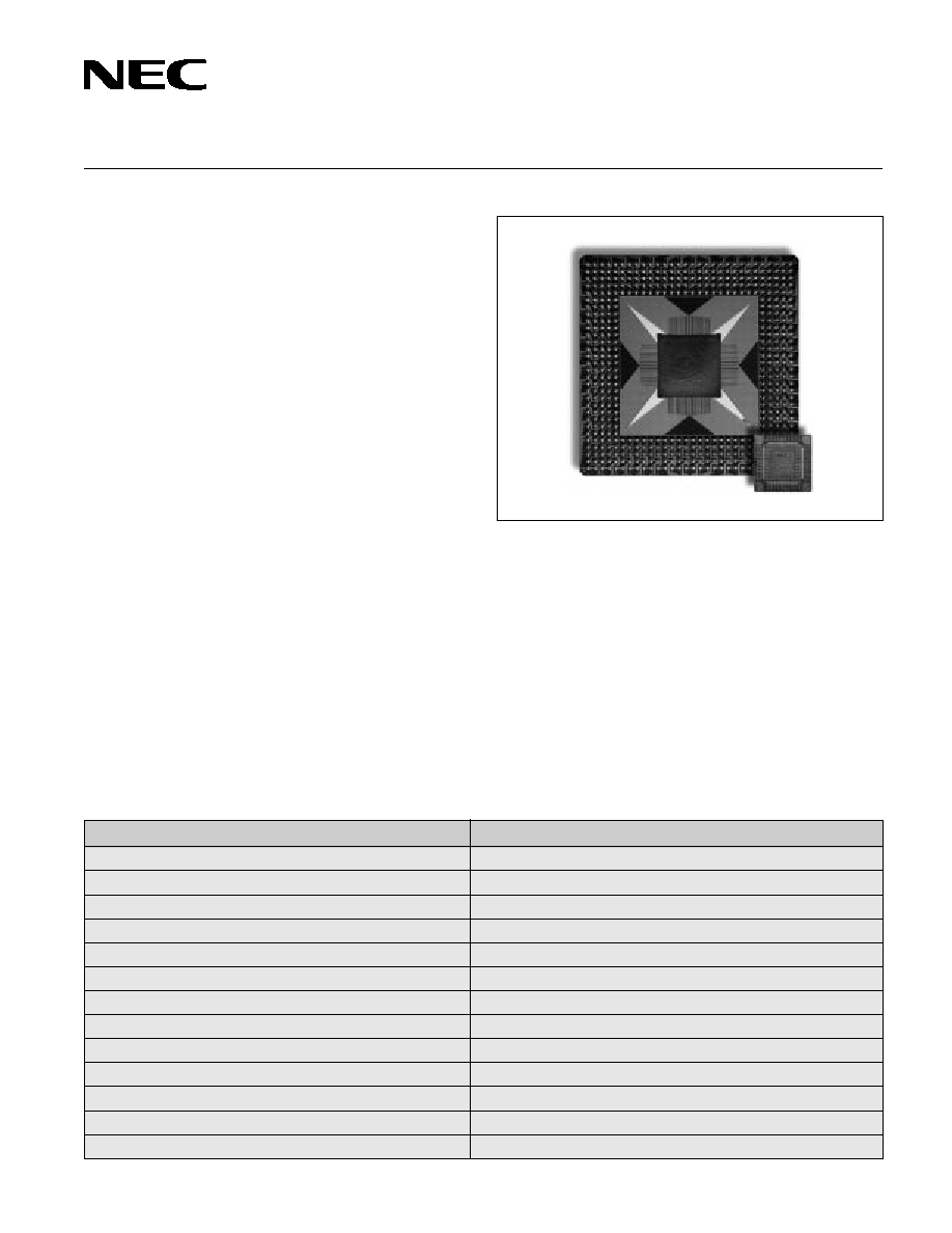
Figure 1. Tape BGA and Chip Size Package
OpenCAD is a registered trademark of NEC Electronics Inc.
All non-NEC trademarks are the property of their respective owners.
Applications
The CMOS-9HD family is ideal for use in enterprise
systems, engineering workstations, telecommunications
switching, transmission and wireless systems, where
extensive integration, high speeds and high density are the
primary design goals. CMOS-9HD is well-suited for
designs requiring very high integration (500K-800K gates,
500-700 pins), high system speeds (100-200 MHz) and
high performance interface standards (GTL+, pECL).
CMOS-9HD is also well-suited for low power applications
where high performance is required.
Table 1. CMOS-9HD Series Features and Benefits
CMOS-9HD Series Features
CMOS-9HD Series Benefits
∑
0.35 µm (drawn) 3-level metal CMOS technology
Delivers high 0.35 µm technology speeds at 2.5 times the density
∑
High-Density NXT Cell Architecture from In-Chip Systems, Inc.
Reduces cell area by 58% resulting in a much lower die cost
∑
Ten base arrays with 76K - 1.6M raw gate counts
Allows several different masters across large range of gate counts
∑
Narrow pad pitch with 156 - 692 available I/Os
Offers large numbers of I/Os with very small die sizes
∑
GTL, GTL+, pECL, and HSTL interface capabilities
Provides signaling with high-speed memory and processor buses
∑
Full range of 5V-protected I/O buffers
Delivers 5V interface capabilities while protecting 3.3V core logic
∑
PCI buffers including 3.3V 66 MHz
Supports the PCI local bus applications
∑
Stacked vias and tighter metal pitch for increased routability
Frees up additional routing area allowing much higher utilization
∑
Single frequency and multiplying DPLL macros
Offers frequency multiplication while eliminating clock tree delay
∑
Low power dissipation: 0.5 µW/MHz/gate
Provides low power consumption at high system clock rates
∑
Extensive package offering: QFPs, BGAs, TAB BGAs, CSPs
Satisfies electrical, thermal, soldering, size and cost requirements
∑
Floorplanner and Clock Tree Synthesis Tool design automation
Optimizes placement and performance while reducing design time
∑
Popular, third-party CAE tools supported
Enables a smooth flow from customer design to silicon
Description
NEC's CMOS-9HD, density-enhanced, 0.35 µm gate array
family delivers a complete, low-cost answer to modern-day
computer and communication system ASICs. This new
family uses the high-speed capabilities of a 3.3V, 0.35 µm
gate array technology, combined with a unique, high-
density NXT architecture from In-Chip Systems, Inc. to
provide an inexpensive, high-performance solution to
demanding design implementations. CMOS-9HD offers
three layers of metal and stacked vias for greater routability
and gate utilization. In addition, many specialized I/Os
allow this densified 0.35 µm family to interface using high-
speed standards such as GTL+, HSTL, pECL and 5 and
3.3V, 66 MHz PCI.
CMOS-9HD also offers an advanced clock insertion
methodology. This includes a progressive clock tree
synthesis capability with high-accuracy single frequency
and multiplying digital phase-locked loops (DPLL).
The CMOS-9HD gate array family consists of 10 available
masters with 76K to 1.6M raw gates. This allows 53K to
1.1M usable gates running on a 3.3V power supply.
CMOS-9HD, as well as the other gate array families,
are supported by NEC's OpenCAD
Æ
design system; a
mixture of popular third-party CAE tools, and proprietary
NEC tools. NEC proprietary tools include GALET
floorplanner which helps reduce layout time and improve
performance, clock tree synthesis for clock skew minimi-
zation, and table lookup delay calculator for accurate
timing characteristics.
CMOS-9HD
2
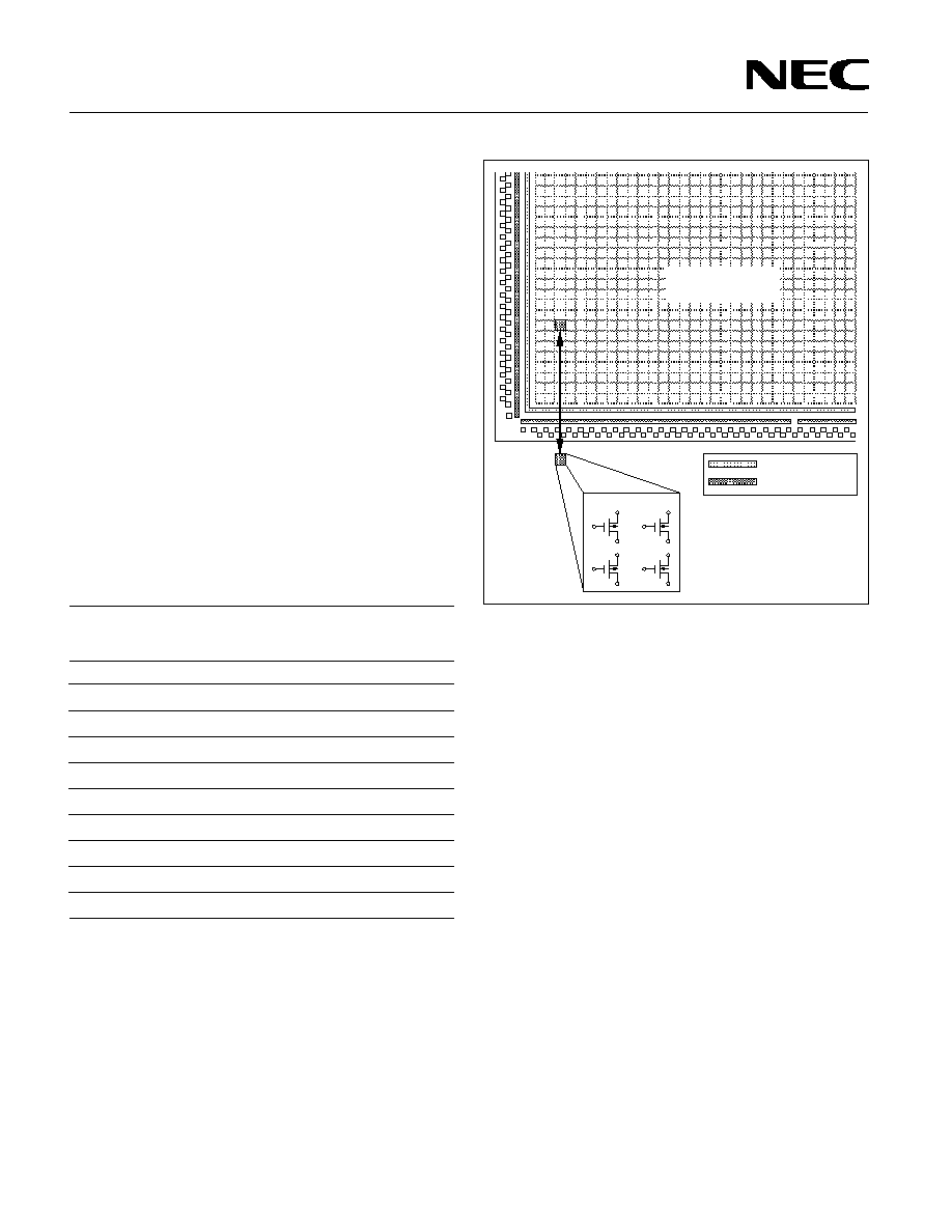
Figure 2. Power Rail Structure
Drawing not to scale
Array Architecture
The CMOS-9HD gate array family is built with In-Chip's
0.35-micron (drawn) channelless array architecture and
NEC's I/O and Power Rail Structure. As shown in
Figure 2, the array is divided into I/O and core regions. The
I/O region contains input and output buffers. The core
region contains the sea-of-gates array and embedded
blocks.
The CMOS-9HD gate array's architecture provides extra
flexibility for high performance system designs. As shown
in Figure 2, the arrays contain two power rails: a 3.3V rail,
and a second power rail (V
DD2
) for special I/O types.
The V
DD2
rail is used for interfaces such as HSTL where
a very low I/O power supply is required (1.4 to 1.6V).
All four classes of HSTL buffer are supported.
The V
DD2
rail may be separated into sections to allow one
device to support two or more buses requiring special I/O
voltages. Examples of spread I/O cells that may use this
V
DD
rail are HSTL and 5V PCI. Each section can operate
as an independent voltage zone, and sections can be
linked together to form common voltage zones.
3.3V VDD Rail
VDD2
Core Region
P-Channel
N-Channel
In-Chip Systems, Inc. joins NEC in the development of
CMOS-9HD's core region. By designing uniquely shaped
transistors which consume a much smaller area, In-Chip is
able to reduce cell size and power while maintaining
advanced 0.35 µm system performance.
CMOS-9HD Memory
CMOS-9HD offers three different types of available memory.
Included are fixed RAM (Random Access Memory) and
ROM (Read Only Memory) blocks, and one- and two-port
compiled RAMs. Each storage element is considered to
be asynchronous in operation.
NEC's high-speed, RAM Blocks have a bit/word architec-
ture based on basic hard macros. The BIST (Built-in-Self-
Test) circuit and built-in selector are configured by soft
macros. This architecture eases restrictions on place-
ment and routing and reduces complexity when multiple
RAMs are placed.
Compiled RAM differs from the conventional RAM in that
the customer can select the bit size in the range from 2 bits
to 128 bits (however, the number of words is limited by the
number of bits).
Table 3 shows the ranges for the existing CMOS-9HD RAM
line-up.
Table 2. CMOS-9HD Base Array Line-up
Device
(1)
Max Pads
(µPD659xx)
Available
Usable Gates
(2)
Reg.
Tight
3LM
Gates
3LM
Pitch
Pitch
43
75740
53018
128
172
44
100602
70421
148
196
45
128338
89836
-
216
46
202630
141841
200
268
48
312684
218878
247
324
49
437136
305995
289
380
51
585390
351234
328
436
54
835664
501398
388
516
56
1096452
657871
445
588
58
1615646
969387
535
708
Notes:
(1) "3LM" represents three-layer metal.
(2) Actual gate utilization varies depending on circuit implementation.
Utilization is 70% for most masters.
Core Region
The core region consists of an array of gates. Each gate
contains 2 n-channel and 2 p-channel MOS logic transis-
tors. One core gate is equivalent to one 2-input NAND gate
(L302).
3
CMOS-9HD
three features to control clock skew: the standard Digital
PLL (DPLL) working at frequencies up to 100 MHz for chip-
to-chip skew minimization, the multiplying digital PLL
providing frequencies up to 200 MHz, and Clock Tree
Synthesis (CTS).
CTS -- supported by an NEC proprietary
design tool -- is used for clock skew management through
the automatic insertion of a balanced buffer tree. The clock
tree insertion method minimizes large-capacitive trunks
and is especially useful with the hierarchical, synthesized
design style being used for high-integration devices. RC
values for actual net lengths of the clock tree are used for
back annotation after place and route operations. A skew
as low as ±100 ps can be achieved.
Accurate Design Verification.
Nonlinear timing calculation
is a very important requirement of the high-density, deep
sub-micron ASIC designs. NEC makes use of the increased
accuracy delivered by the nonlinear table look-up delay
calculation methodology and offers consistent wire load
models to ensure a high accuracy of the design verification.
Design Rule Check. A comprehensive design rule check
(DRC) program reports design rule violations as well as
chip utilization statistics for the design netlist.
The generated report contains such information as net
counts, total pin and gate counts, and utilization figures.
Layout. During design synthesis, wire load models are
used to get delay estimations in a very early state of the
design flow. In general, there's no need for customers to
perform the floorplanning to meet the required timing.
During layout, enhanced in-place optimization (IPO)
features of the layout tools and engineering change order
(ECO) capabilities of the synthesis tools are used to
optimize critical timing paths defined by the given timing
constraints. This feature can reduce the total design time.
Test Support
The CMOS-9HD family supports automatic test generation
through a scan test methodology. It includes internal scan,
boundary scan (JTAG) and built-in-self-test (BIST)
architecture for easy and high-performance production
RAM testing. This allows higher fault coverage, easier
testing and faster development time.
Supplemental Publications
This data sheet contains preliminary specifications and
operational data for the CMOS-9HD gate array family.
Additional information is available in NEC's CMOS-9HD
Design Manual, Block Library, Memory Macro Design
Manual and other related documents.
Please call your local NEC design center for additional
information; see the back of this data sheet for locations
and telephone numbers.
Table 3. CMOS-9HD RAM Types
Type
M o d e
Ports
Bit Range
Word Range
Compiled
Sync.
1
2-128 bits
4-1K words
2-word incr.
Sync.
2
2-128 bits
4-1K words
2-word incr.
Block
High-speed
1
4-10 bits
16-64 words
Sync.
High-speed
2
4-10 bits
16-64 words
Sync.
High-Speed
1
4-10 bits
16-64 words
Async.
High-Speed
2
4-10 bits
16-64 words
Async.
Packaging and Test
CMOS-9HD gate arrays support automatic test generation
through a scan-test methodology, which allows higher fault
coverage, easier testing and quicker development time.
NEC also offers optional BIST test structures for RAM
testing.
NEC offers advanced packaging solutions including Tape
Ball Grid Arrays (TBGA), Plastic Ball Grid Arrays (PBGA),
Fine Pitch Ball Grid Arrays (FPBGA), Chip Size Packages
(CSP), Plastic Quad Flat Packages (PQFP), Low Profile
Plastic Quad Flat Packages (LQFP), Thin Plastic Quad
Flat Packages (TQFP), and Pin Grid Arrays (PGA).
Please call your local NEC ASIC Design Center for a listing
of available master/package combinations.
CAD Support
The CMOS-9HD family is fully supported by NEC's
sophisticated OpenCAD
Æ
design framework, CMOS-9HD
maximizes design quality and flexibility while minimizing
ASIC design time.
NEC's OpenCAD system allows designers to combine the
EDA industry's most popular third-party design tools with
proprietary NEC tools, including those for advanced
floorplanner, clock tree synthesis, automatic test pattern
generation (ATPG), full-timing simulation, accelerated
fault grading and advanced place and route algorithms.
The latest OpenCAD system is open for sign-off using
standard EDA tools. NEC offers RTL- and STA- (Static
Timing Analysis) sign-off procedures to shorten the ASIC
design cycle of high-complexity designs.
Support of High-Speed Systems. High-speed systems
require tight control of clock skew on the chip and between
devices on a printed circuit board. CMOS-9HD provides
CMOS-9HD
4
Absolute Maximum Ratings
Power supply voltage, V
DD
≠0.5 to +4.6 V
Input Voltage, V
I
3V Input buffer (at V
I
< V
DD
+ 0.5V)
-0.5 to 4.6 V
3V Fail-safe input buffer (at V
I
< V
DD
+ 0.5V)
-0.5 to 4.6 V
5V Input buffer (at V
I
< V
DD
+ 5.0V)
-0.5 to 6.6 V
Output Voltage, V
O
3V Output buffer (at V
O
< V
DD
+ 0.5V)
-0.5 to 4.6 V
5V TTL Output buffer (at V
O
< V
DD
+ 3.0V)
-0.5 to 6.6 V
5V CMOS Output buffer (at V
O
< V
DD
+ 3.0V)
-0.5 to 6.6 V
Latch-up current, I
LATCH
>1 A (typ)
Operating temperature, T
OPT
-40 to +85∞C
Storage temperature, T
STG
-65 to +150∞C
Input/Output Capacitance
V
DD
= V
I
= 0 V; f = 1 MHz
Terminal
Symbol
Min
Typ
Max
Unit
3V
2.2*
3.3*
Input
C
IN
pF
5V
4.4*
5.5*
3V
2.2*
3.3*
Output
C
OUT
pF
5V
4.4*
5.5*
3V
2.2*
3.3*
I/O
C
I/O
pF
5V
4.4*
5.5*
Notes:
Values include package pin capacitance.
*Estimated
Recommended Operating Conditions
3.3V Interface 5V Interface
5V PCI 3.3V PCI
Block
Block
Level
Level
Parameter
Symbol
Min
Max
Min
Max
Min
Max
Min
Max
Unit
I/O Power supply voltage
V
DD
3.0
3.6
3.0
3.6
3.0
3.6
3.0
3.6
V
Junction temperature
T
J
-40
+125
-40
+125
-40
+125
-40
+125
∞C
High-level input voltage
V
IH
2.0
V
DD
2.0
5.5
2.0
V
CC
0.5V
CC
V
CC
V
Low-level input voltage
V
IL
0
0.8
0
0.8
0
0.8
0
0.3V
CC
V
Positive trigger voltage
V
P
12
2.4
1.2
2.4
--
--
--
--
V
Negative trigger voltage
V
N
0.6
1.8
.6
1.8
--
--
--
--
V
Hysteresis voltage
V
H
.3
1.5
.3
1.5
--
--
--
--
V
Input rise/fall time
t
R
, t
F
0
1
0
1
0
1
0
1
ns
Input rise/fall time, Schmitt
t
R
, t
F
0
1
0
1
--
--
--
--
ms
Power Consumption
Description
Limits
Unit
Internal gate
.65*
µW/MHz
Input buffer (FI01)
4.03*
µW/MHz
Output buffer (FO01 @ 15 pF)
140*
µW/MHz
Caution: Exposure to absolute maximum ratings for extended periods may
affect device reliability; exceeding the ratings could cause permanent damage.
The device should not be operated outside the recommended operating
conditions.
*Estimated
AC Characteristics
V
DD
= 3.3V ± 0.3V; T
j
= -40 to +125∞C
Parameter
Symbol
Min
Typ
Max
Unit
Conditions
Toggle frequency (D-flip-flop)
f
TOG
670
MHz
F/O = 2, 5V
Delay time, 2-input NAND gate @ 5V
94
ps
F/O = 1; L = 0 mm
13.1
ps
F/O = 1; L = .15 mm/pin pair
Standard gate (F302)
t
PD
108
ps
F/O = 2; L = 0 mm
107
ps
F/O = 1; L = .15 mm/pin pair
Power gate (F322)
t
PD
94
ps
F/O = 2; L = 0 mm
Delay time, buffer
Input buffer (FI01)
t
PD
229
ps
F/O = 1; L = .15 mm/pin pair
Input buffer (FI01)
t
PD
222
ps
F/O = 2; L = 0 mm
Output buffer (FO01)
t
PD
1.4
ns
C
L
= 15 pF
Output rise time (FO01)
t
R
2.39
ns
C
L
= 15 pF
Output fall time (FO01)
t
F
1.87
ns
C
L
= 15 pF
5
CMOS-9HD
Notes:
(1) Static current consumption increases if an I/O block with on-chip pull-up/
pull-down resistor or an oscillator is used. Contact an NEC ASIC Design
Center for assistance in calculation.
(2) Leakage current is limited by tester capabilities. Specification listed represents
this measurement limitation. Actual values will be significantly lower.
(3) Rating is for only one output operating in this mode for less than 1 second.
(4) Resistor is called 50k
for backwards compatibility.
DC Characteristics
V
DD
= 3.3V ± 0.3V; T
j
= -40 to +125∞C
Parameter
Symbol
Min
Typ
Max
Unit
Conditions
Quiescent current (µPD654xx)
(1)
-19, -39
I
DDS
2.0
300
µA
V
I
= V
DD
or GND
-17, -37, -15, -35, -13, -33, -11, -31
I
DDS
2.0
300
µA
V
I
= V
DD
or GND
-10, -30, -09, -29, -08, -28
I
DDS
2.0
300
µA
V
I
= V
DD
or GND
-06, -26, -07, -27
I
DDS
2.0
300
µA
V
I
= V
DD
or GND
Off-state output leakage current
3V output buffer
I
OZ
±10
µA
V
O
= V
DD
or GND
5V-protected TTL buffer
I
OZ
±10
µA
V
O
= V
DD
or GND
Output short circuit current
(3)
I
OS
-250
mA
V
O
= GND
Input leakage current
(2)
Regular
I
I
±10
≠4
±10
µA
V
I
= V
DD
or GND
50 k
pull-up
I
I
28
83
190
µA
V
I
= GND
5 k
pull-up
I
I
280
700
1900
µA
V
I
= GND
50 k
pull-down
I
I
28
83
190
µA
V
I
= V
DD
Resistor values
50 k
pull-up
(4)
R
pu
21.8
37.1
83.1
k
5 k
pull-up
R
pu
2.8
5.0
10.6
k
50 k
pull-down
R
pu
25.6
41.9
105.8
k
Low-level output current (5V Interface Block)
1 mA
I
OL
1
mA
V
OL
= 0.4 V
2 mA
I
OL
2
mA
V
OL
= 0.4 V
3 mA
I
OL
3
mA
V
OL
= 0.4 V
6 mA
I
OL
6
mA
V
OL
= 0.4 V
9 mA
I
OL
9
mA
V
OL
= 0.4 V
12 mA
I
OL
12
mA
V
OL
= 0.4 V
High-level output current (5V Interface Block)
1 mA
I
OH
≠1
mA
V
OH
= 2.4 V
2 mA
I
OH
≠1
mA
V
OH
= 2.4 V
3 mA
I
OH
≠3
mA
V
OH
= 2.4 V
6 mA
I
OH
≠3
mA
V
OH
= 2.4 V
9 mA
I
OH
≠3
mA
V
OH
= 2.4 V
12 mA
I
OH
≠3
mA
V
OH
= 2.4 V
Low-level output current (3.3V Interface Block)
3 mA (FO09)
I
OL
3.0
TBD
mA
V
OL
= 0.4 V
6 mA (FO04)
I
OL
6.0
TBD
mA
V
OL
= 0.4 V
9 mA (FO01)
I
OL
9.0
TBD
mA
V
OL
= 0.4 V
12 mA (FO02)
I
OL
12.0
TBD
mA
V
OL
= 0.4 V
18 mA (FO03)
I
OL
18.0
TBD
mA
V
OL
= 0.4 V
24 mA (FO06)
I
OL
24.0
TBD
mA
V
OL
= 0.4 V
High-level output current (3.3V Interface Block)
3 mA (FO09)
I
OH
-3
mA
V
OH
= 2.4 V
6 mA (FO04)
I
OH
-6
mA
V
OH
= 2.4 V
9 mA (FO01)
I
OH
-9
mA
V
OH
= 2.4 V
12 mA (FO02)
I
OH
-12
mA
V
OH
= 2.4 V
18 mA (FO03)
I
OH
-18
mA
V
OH
= 2.4 V
24 mA (FO06)
I
OH
-24
mA
V
OH
= 2.4 V
Low-level output voltage
V
OL
0.1
V
I
OL
= 0 mA
High-level output voltage
V
OH
V
DD
-0.1
V
I
OH
= 0 mA