
LMH0034
SMPTE 292M / 259M Adaptive Cable Equalizer
General Description
The LMH0034 SMPTE 292M / 259M adaptive cable equal-
izer is a monolithic integrated circuit for equalizing data
transmitted over cable (or any media with similar dispersive
loss characteristics). The equalizer operates over a wide
range of data rates from 143 Mbps to 1.485 Gbps and
supports SMPTE 292M, SMPTE 344M and SMPTE 259M.
The LMH0034 implements DC restoration to correctly handle
pathological data conditions. DC restoration can be by-
passed for low data rate applications. The equalizer is flex-
ible in allowing either single-ended or differential input drive.
Additional features include a combined carrier detect and
output mute pin which mutes the output when no signal is
present. A programmable mute reference is used to mute the
output at a selectable level of signal degradation. A cable
length indicator is provided to determine the amount of cable
being equalized.
Features
n
SMPTE 292M, SMPTE 344M and SMPTE 259M
compliant
n
Supports DVB-ASI at 270 Mbps
n
High data rates: 143 Mbps to 1.485 Gbps
n
Equalizes up to 200 meters of Belden 1694A at 1.485
Gbps or up to 400 meters of Belden 1694A at 270 Mbps
n
Manual bypass, cable length indicator, and output mute
with a programmable threshold
n
Single-ended or differential input
n
50
differential outputs
n
Single 3.3V supply operation
n
208mW typical power consumption with 3.3V supply
n
Replaces the GS1524 and GS1524A
Applications
n
SMPTE 292M, SMPTE 344M, and SMPTE 259M serial
digital interfaces
n
Serial digital data equalization and reception
n
Data recovery equalization
Typical Application
20173401
June 2006
LMH0034
SMPTE
292M
/
259M
Adaptive
Cable
Equalizer
� 2006 National Semiconductor Corporation
DS201734
www.national.com
Absolute Maximum Ratings
(Note 1)
Supply Voltage
-0.5V to 3.6V
Input Voltage (all inputs)
-0.3V to V
CC
+0.3V
Storage Temperature Range
-65�C to +150�C
Junction Temperature
+150�C
Lead Temperature
(Soldering 4 Sec)
+260�C
Package Thermal Resistance
JA
16-pin SOIC
JC
16-pin SOIC
+115�C/W
+105�C/W
ESD Rating (HBM)
8kV
ESD Rating (MM)
250V
Recommended Operating
Conditions
Supply Voltage (V
CC
� V
EE
)
3.3V
�
5%
Input Coupling Capacitance
1.0 �F
AEC Capacitor (Connected between
AEC+ and AEC-)
1.0 �F
Operating Free Air Temperature (T
A
)
0�C to +85�C
DC Electrical Characteristics
Over Supply Voltage and Operating Temperature ranges, unless otherwise specified (Notes 2, 3).
Symbol Parameter
Conditions
Reference
Min
Typ
Max
Units
V
CMIN
Input Common Mode Voltage
SDI, SDI
1.9
V
V
SDI
Input Voltage Swing
At LMH0034 input, (Notes 4, 6)
720
800
950
mV
P-P
V
CMOUT
Output Common Mode Voltage
SDO, SDO
V
CC
�
V
SDO
/2
V
V
SDO
Output Voltage Swing
50
load, differential
750
mV
P-P
CLI DC Voltage
0m cable
CLI
2.5
V
Max cable
1.6
V
MUTE
REF
DC Voltage (floating)
MUTE
REF
1.3
V
MUTE
REF
Range
0.7
V
CD/MUTE Output Voltage
Carrier not present
CD/MUTE
2.6
V
Carrier present
0.4
V
CD/MUTE Input Voltage
Min to mute outputs
3.0
V
Max to force outputs active
2.0
V
I
CC
Supply Current
(Note 7)
63
77
mA
LMH0034
www.national.com
2
AC Electrical Characteristics
Over Supply Voltage and Operating Temperature ranges, unless otherwise specified (Note 3).
Symbol Parameter
Conditions
Reference
Min
Typ
Max
Units
BR
SDI
Input Data Rate
SDI, SDI
143
1485
Mbps
Jitter for various cable lengths
(with equalizer pathological)
270 Mbps, Belden 1694A,
400 meters (Note 4)
0.2
UI
270 Mbps, Belden 8281,
280 meters (Note 4)
0.2
UI
1.485 Gbps, Belden 1694A,
140 meters (Note 4)
0.25
UI
1.485 Gbps, Belden 8281,
100 meters (Note 4)
0.25
UI
1.485 Gbps, Belden 1694A,
200 meters (Note 4)
0.3
t
r
,t
f
Output Rise Time, Fall Time
20% � 80%, (Note 4)
SDO, SDO
100
220
ps
Mismatch in Rise/Fall Time
(Note 4)
2
15
ps
t
OS
Output Overshoot
(Note 4)
1
5
%
R
OUT
Output Resistance
single-ended, (Note 5)
50
RL
IN
Input Return Loss
(Note 8)
SDI, SDI
15
18-20
dB
R
IN
Input Resistance
single-ended
1.3
k
C
IN
Input Capacitance
single-ended, (Note 5)
1
pF
Note 1: "Absolute Maximum Ratings" are those parameter values beyond which the life and operation of the device cannot be guaranteed. The stating herein of
these maximums shall not be construed to imply that the device can or should be operated at or beyond these values. The table of "Electrical Characteristics"
specifies acceptable device operating conditions.
Note 2: Current flow into device pins is defined as positive. Current flow out of device pins is defined as negative. All voltages are stated referenced to V
EE
= 0 Volts.
Note 3: Typical values are stated for V
CC
= +3.3V and T
A
= +25�C.
Note 4: Specification is guaranteed by characterization.
Note 5: Specification is guaranteed by design.
Note 6: The maximum input voltage swing assumes a nonstressing, DC-balance signal; specifically, the SMPTE-recommended color bar test signal. Pathological
or other stressing signals may not be used. This specification is for 0m cable only.
Note 7: Supply current depends on the amount of cable being equalized. The current is highest for short cable and decreases as the cable length is increased. Refer
to Figures 1, 2.
Note 8: Input return loss is dependent on board design. The LMH0034 meets this specification on the SD034 evaluation board from 5MHz to 1.5GHz.
LMH0034
www.national.com
3
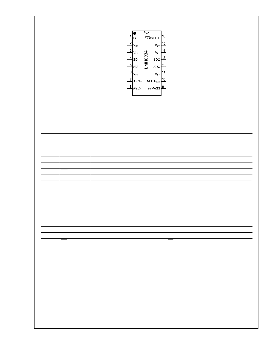
Connection Diagram
20173403
16-Pin SOIC
Order Number LMH0034MA
See NS Package Number M16A
Pin Descriptions
Pin #
Name
Description
1
CLI
Cable length indicator. Provides a voltage inversely proportional to the cable length being
equalized.
2
V
CC
Positive power supply (+3.3V).
3
V
EE
Negative power supply (ground).
4
SDI
Serial data true input.
5
SDI
Serial data complement input.
6
V
EE
Negative power supply (ground).
7
AEC+
AEC loop filter external capacitor (1�F) positive connection.
8
AEC-
AEC loop filter external capacitor (1�F) negative connection.
9
BYPASS
Bypasses equalization and DC restoration when high. No equalization occurs in this mode.
10
MUTE
REF
Mute reference. Determines the maximum cable to be equalized before muting. May be
unconnected for maximum equalization.
11
V
EE
Negative power supply (ground).
12
SDO
Serial data complement output.
13
SDO
Serial data true output.
14
V
EE
Negative power supply (ground).
15
V
CC
Positive power supply (+3.3V).
16
CD/MUTE
Bi-directional carrier detect and output mute. CD/MUTE is high when no signal is present. If
unconnected, MUTE is controlled automatically by carrier detect. To force MUTE on, tie to
V
CC
. To disable MUTE, tie to GND. CD/MUTE has no function in BYPASS mode.
LMH0034
www.national.com
4
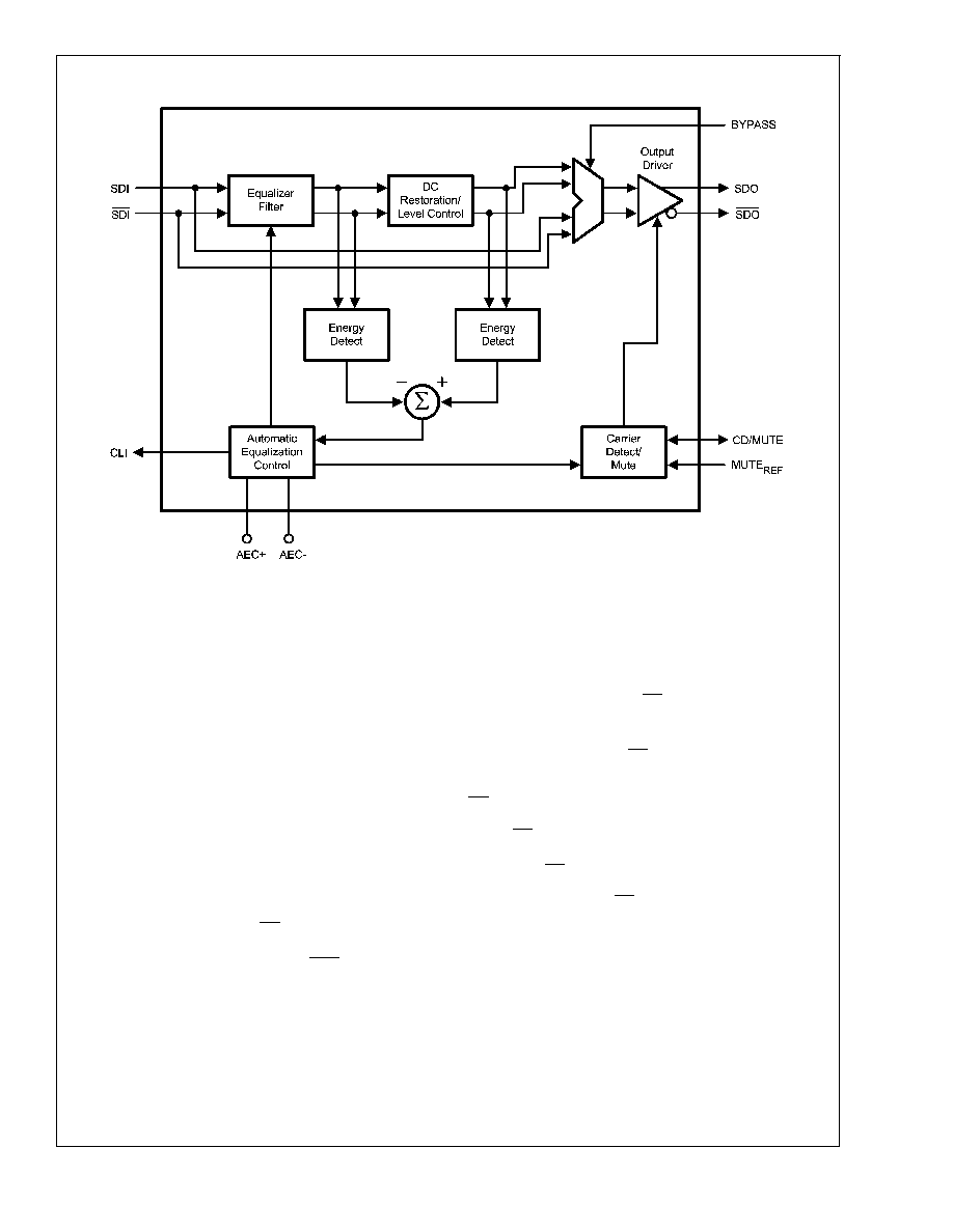
Block Diagram
20173402
Device Operation
BLOCK DESCRIPTION
The Equalizer Filter block is a multi-stage adaptive filter. If
Bypass is high, the equalizer filter is disabled.
The DC Restoration / Level Control block receives the
differential signals from the equalizer filter block. This block
incorporates a self-biasing DC restoration circuit to fully DC
restore the signals. If Bypass is high, this function is dis-
abled.
The signals before and after the DC Restoration / Level
Control block are used to generate the Automatic Equal-
ization Control (AEC) signal. This control signal sets the
gain and bandwidth of the equalizer filter. The loop response
in the AEC block is controlled by an external 1�F capacitor
placed across the AEC+ and AEC- pins. Cable Length
Indicator (CLI) is derived from this block.
The Carrier Detect / Mute block generates the carrier detect
signal and controls the mute function of the output. This
block utilizes the bi-directional CD/MUTE signal along with
Mute Reference (MUTE
REF
).
The Output Driver produces SDO and SDO.
CABLE LENGTH INDICATOR (CLI)
The cable length indicator provides a voltage to indicate the
length of cable being equalized. The CLI voltage decreases
as the cable length increases.
MUTE REFERENCE (MUTE
REF
)
The mute reference determines the amount of cable to
equalize before automatically muting the outputs. This is set
by applying a voltage inversely proportional to the length of
cable to equalize. As the applied MUTE
REF
voltage is in-
creased, the amount of cable that can be equalized before
carrier detect is de-asserted and the outputs are muted is
decreased. MUTE
REF
may be left unconnected for maximum
equalization before muting.
CARRIER DETECT / MUTE (CD/MUTE)
Carrier Detect / Mute is bi-directional, serving as both a
carrier detect (output function) and mute (input function).
When used as an output, CD/MUTE determines if a valid
signal is present at the LMH0034 input. If MUTE
REF
is used,
the carrier detect threshold will be altered accordingly.
CD/MUTE provides a high voltage when no signal is present
at the LMH0034 input, and the outputs are automatically
muted. CD/MUTE is low when a valid input signal has been
detected, and the outputs are automatically enabled.
As an input, CD/MUTE can be used to override the carrier
detect and manually mute or enable the LMH0034 outputs.
Applying a high input to CD/MUTE will mute the LMH0034
outputs. Applying a low input will force the outputs to be
active regardless of the length of cable or the state of
MUTE
REF
.
INPUT INTERFACING
The LMH0034 accepts either differential or single-ended
input. The input must be AC coupled. Transformer coupling
is not supported.
The LMH0034 correctly handles equalizer pathological sig-
nals for standard definition and high definition serial digital
video, as described in SMPTE RP 178 and RP 198, respec-
tively.
LMH0034
www.national.com
5