 | –≠–ª–µ–∫—Ç—Ä–æ–Ω–Ω—ã–π –∫–æ–º–ø–æ–Ω–µ–Ω—Ç: NJG1105F | –°–∫–∞—á–∞—Ç—å:  PDF PDF  ZIP ZIP |

NJG1105F
- 1 -
1.9/2.1GHz LOW NOISE AMPLIFIER GaAs MMIC
n
GENERAL DESCRIPTION
n
PACKAGE OUTLINE
NJG1105F is a Low Noise Amplifier GaAs MMIC
designed for 1.9/2.1GHz digital cellular phone handsets
such as PCS and WCDMA.
This amplifier provides low noise figure, high gain
and high IP3 operated by single low positive power supply.
n
FEATURES
l
Low voltage operation
+2.9V typ.
l
Low current consumption
6mA typ.
l
Small Package
MTP6 (Mount Size: 2.8x2.9x1.2mm)
[1.8GHz Band]
l
High small signal gain
20dB typ. @f=1860MHz
l
Low Noise Figure
1.3dB typ. @f=1860MHz
l
High Input IP3
-3dBm typ. @f=1860.0+1860.1MHz
[1.9GHz Band]
l
High small signal gain
20dB typ. @f=1960MHz
l
Low Noise Figure
1.3dB typ. @f=1960MHz
l
High Input IP3
-2dBm typ. @f=1960.0+1960.1MHz
[2.1GHz Band]
l
High small signal gain
16dB typ. @f=2140MHz
l
Low Noise Figure
1.3dB typ. @f=2140MHz
l
High Input IP3
0dBm typ. @f=2140.0+2140.1MHz
n
PIN CONFIGURATION
NJG1105F
(Top View)
Orientation Mark
1
2
3
4
5
6
Pin connection
1.VDD
2.GND
3.RF OUT
4.RF IN
5.GND
6.EXTCAP
Ver 1 12/25'99
TENTATIVE

NJG1105F
- 2 -
n
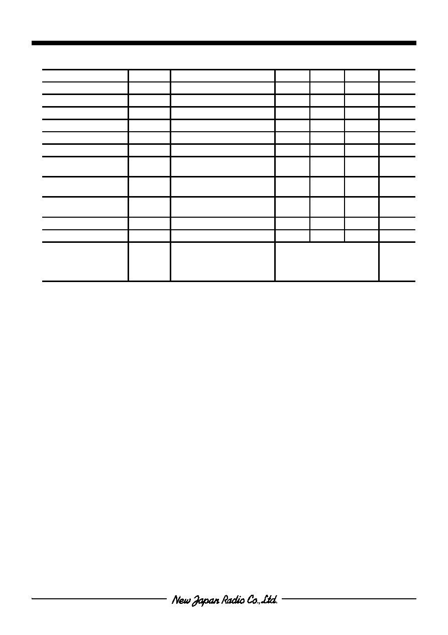
ABSOLUTE MAXIMUM RATINGS
(T
a
=+25∞C, Z
s
=Z
l
=50
)
PARAMETER
SYMBOL
CONDITIONS
RATINGS
UNITS
Drain Voltage
V
DD
6.5
V
Input Power
Pin
V
DD
=2.9V
+15
dBm
Power Dissipation
P
D
150
mW
Operating Temp.
T
opr
-40~+85
∞C
Storage Temp.
T
stg
-55~+125
∞C
n
ELECTRICAL CHARACTERISTICS 1 (1.8GHz Band)
(V
DD
=2.9V, f=1860MHz, T
a
=+25∞C, Z
s
=Z
l
=50
)
PARAMETER
SYMBOL
CONDITIONS
MIN
TYP
MAX
UNITS
Operating Frequency
Freq
1840
1860
1870
MHz
Drain Voltage
V
DD
2.7
2.9
5.5
V
Operating Current
I
DD
RF OFF
-
6.0
8.0
mA
Small Signal Gain
Gain
17.0
20.0
23.0
dB
Gain Flatness
G
flat
f=1840~1870MHz
-
0.5
1.0
dB
Noise Figure
NF
-
1.3
1.6
dB
Pout at 1dB Gain
Compression point
P
-1dB
+2.0
+4.0
-
dBm
Input 3rd Order
Intercept Point
IIP3
f=1860.0+1860.1MHz
-5.0
-3.0
-
dBm
Output 3rd Order
Intercept Point
OIP3
f=1860.0+1860.1GHz
+15
+17
LNAIN Port VSWR
VSWR
i
-
1.5
2.0
LNAOUT Port VSWR
VSWR
o
-
1.5
2.0
STABILITY
Input and output
terminal: open or short,
No RF input, T
a
=20~80∞C,
freq<20GHz
Spurious: -60dBm max.
No return gain
NOTE: External circuits are required to get electrical characteristics
Above at specified frequency.

NJG1105F
- 3 -
n
ELECTRICAL CHARACTERISTICS 2 (1.9GHz Band)
(V
DD
=2.9V, f=1960MHz, T
a
=+25∞C, Z
s
=Z
l
=50
)
PARAMETER
SYMBOL
CONDITIONS
MIN
TYP
MAX
UNITS
Operating Frequency
Freq
1930
1960
1990
MHz
Drain Voltage
V
DD
2.7
2.9
5.5
V
Operating Current
I
DD
RF OFF
-
6.0
8.0
mA
Small Signal Gain
Gain
17.0
20.0
23.0
dB
Gain Flatness
G
flat
f=1930~1990MHz
-
0.5
1.0
dB
Noise Figure
NF
-
1.3
1.6
dB
Pout at 1dB Gain
Compression point
P
-1dB
+3.0
+5.0
-
dBm
Input 3rd Order
Intercept Point
IIP3
f=1960.0+1960.1MHz
-4.0
-2.0
-
dBm
Output 3rd Order
Intercept Point
OIP3
f=1960.0+1960.1MHz
+16
+18
LNAIN Port VSWR
VSWR
i
-
1.5
2.0
LNAOUT Port VSWR
VSWR
o
-
1.5
2.0
STABILITY
Input and output
terminal: open or short,
No RF input, T
a
=20~80∞C,
freq<20GHz
Spurious: -60dBm max.
No return gain
NOTE: External circuits are required to get electrical characteristics
Above at specified frequency.
NJG1105F
- 4 -
n
ELECTRICAL CHARACTERISTICS 3 (2.1GHz Band)
(V
DD
=2.9V, f=2140MHz, T
a
=+25∞C, Z
s
=Z
l
=50
)
PARAMETER
SYMBOL
CONDITIONS
MIN
TYP
MAX
UNITS
Operating Frequency
Freq
2110
2140
2170
MHz
Drain Voltage
V
DD
2.7
2.9
5.5
V
Operating Current
I
DD
RF OFF
-
6.0
8.0
mA
Small Signal Gain
Gain
13.0
16.0
19.0
dB
Gain Flatness
G
flat
f=2110~2140MHz
-
0.5
1.0
dB
Noise Figure
NF
-
1.3
1.6
dB
Pout at 1dB Gain
Compression point
P
-1dB
+3.0
+5.0
-
dBm
Input 3rd Order
Intercept Point
IIP3
f=2140.0+2140.1MHz
-2.0
0.0
-
dBm
Output 3rd Order
Intercept Point
OIP3
f=2140.0+2140.1MHz
+17
+19
LNAIN Port VSWR
VSWR
i
-
1.5
2.0
LNAOUT Port VSWR
VSWR
o
-
1.5
2.0
STABILITY
Input and output
terminal: open or short,
No RF input, T
a
=20~80∞C,
freq<20GHz
Spurious: -60dBm max.
No return gain
NOTE: External circuits are required to get electrical characteristics
Above at specified frequency.

NJG1105F
- 5 -
n
PACKAGE OUTLINE (MTP6)
Lead material
: Copper
Lead surface finish : Solder plating
Molding material
: Epoxy resin
Unit
: mm
Weight
: 14mg
Cautions on using this product
This product contains Gallium-Arsenide (GaAs) which is a harmful material.
∑
Do NOT eat or put into mouth.
∑
Do NOT dispose in fire or break up this product.
∑
Do NOT chemically make gas or powder with this product.
∑
To waste this product, please obey the relating law of your country.
This product may be damaged with electric static discharge (ESD) or spike voltage. Please handle
with care to avoid these damages.
[CAUTION]
The specifications on this databook are only
given for information , without any guarantee
as regards either mistakes or omissions. The
application circuits in this databook are
described only to show representative usages
of the product and not intended for the
guarantee or permission of any right including
the industrial rights.