NJG1512V
- 1 -
SPDT SWITCH GaAs MMIC
n
GENERAL DESCRIPTION
n
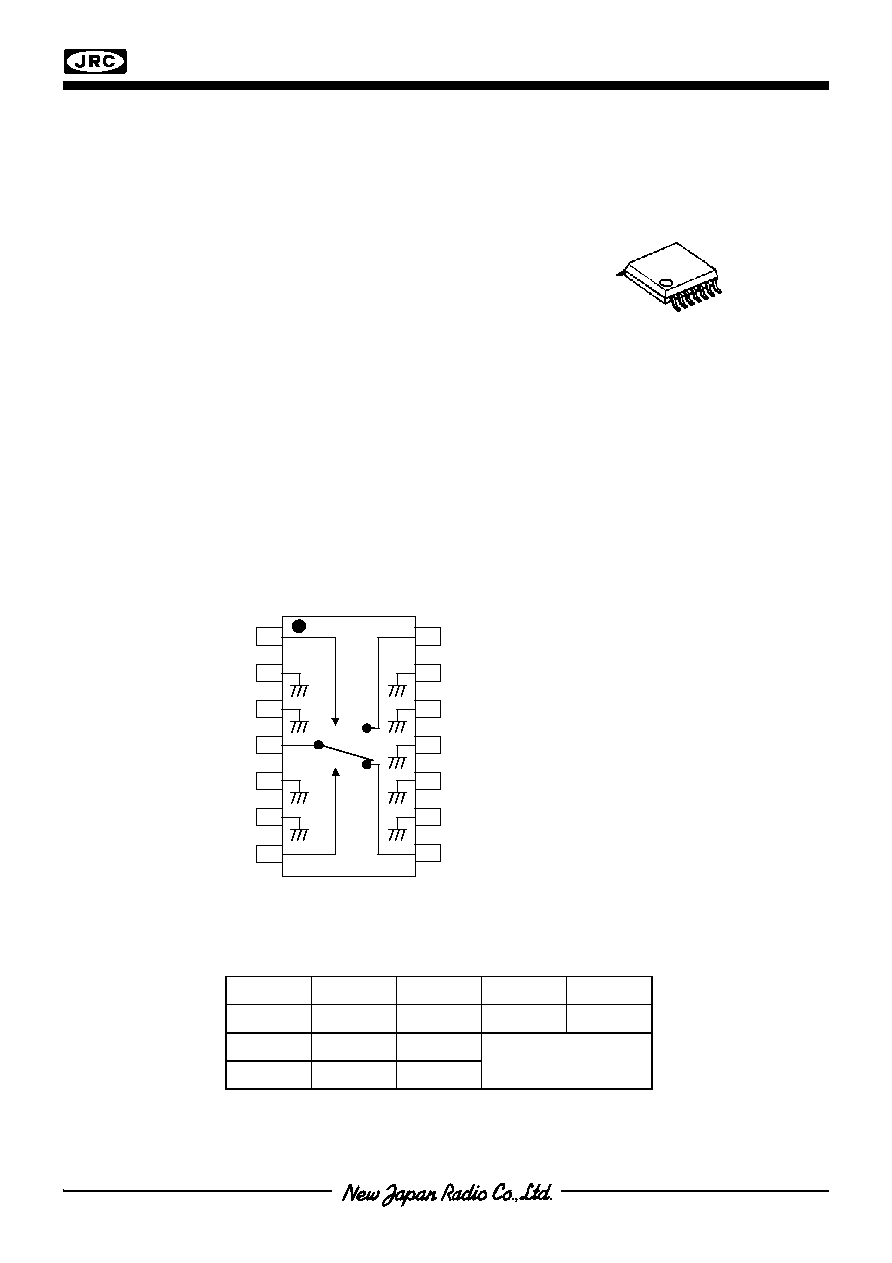
PACKAGE OUTLINE
NJG1512V is a GaAs SPDT switch IC featuring high
isolation and low insertion loss.
This switch allows low operating voltage from 2.5V at
the wide frequency range from 1MHz to 3GHz.
NJG1512V is suitable to switch the synthesizer
signals between transmit and receiving circuit.
A very small SSOP package is adopted.
n
FEATURES
l
Single, low voltage control
+2.5~+5.5V
l
High isolation
46dB typ. @f=0.05~2GHz, P
in
=0dBm
l
Low insertion loss
0.8dB typ. @f=2GHz, P
in
=0dBm
l
Low current consumption
2uA typ. @f=0.05~2.5GHz, P
in
=10dBm
l
Package
SSOP14 (Mount Size: 6.4x5.0x1.25mm)
n
PIN CONFIGURATION
n
TRUTH TABLE
V
CTR1
H
L
L
H
V
CTR2
L
H
L
H
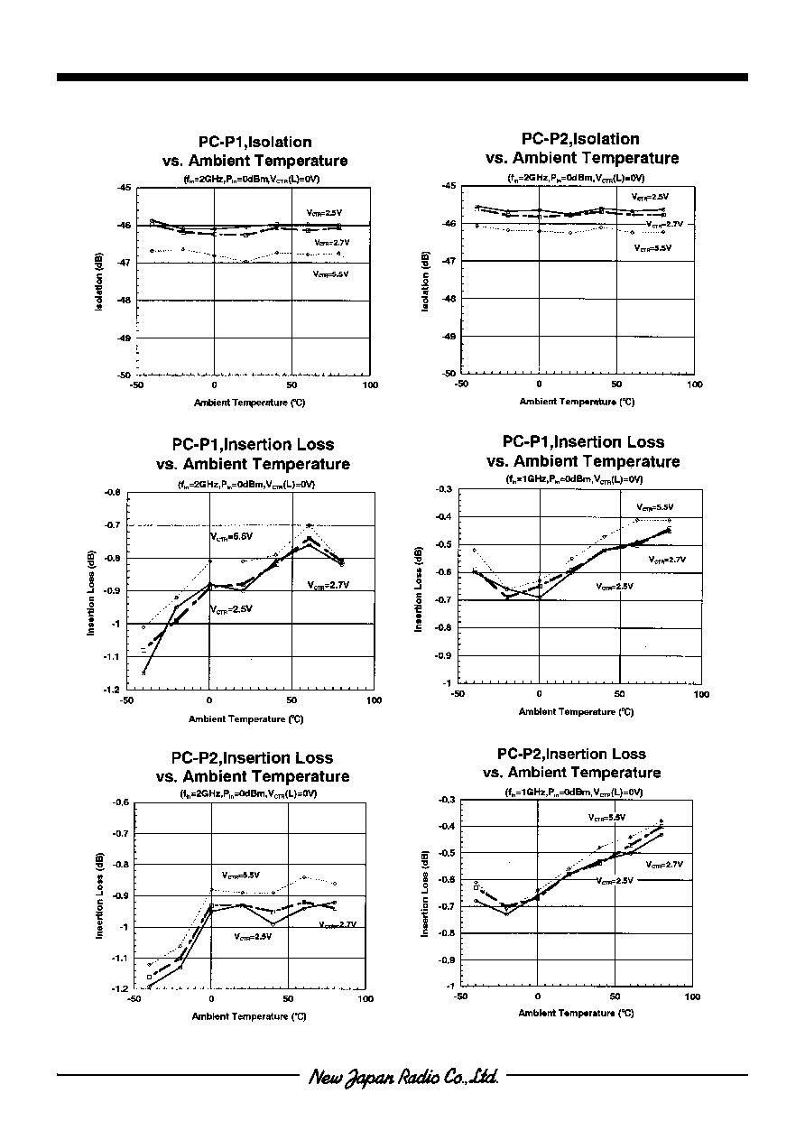
PC-P1
OFF
ON
PC-P2
ON
OFF
*1
"H"=V
CTR (H),
"L"=V
CTR (L)
NJG1512V
*1) Combinations of V
CTR1
/V
CTR2
=L/L, H/H are not available.
Pin Connection
1. V
CTR2
2. GND
3. GND
4. PC
5. GND
6. GND
7. V
CTR1
8. P1
9. GND
10. GND
11. GND
12. GND
13. GND
14. P2
V Type
(Top View)
1
2
3
4
5
6
7
14
13
12
11
10
9
8
NJG1512V
- 2 -
n
ABSOLUTE MAXIMUM RATINGS
(T
a
=25�C, Z
s
=Z
l
=50
)
PARAMETER
SYMBOL
RATINGS
UNITS
Input Power
P
in
27
dBm
Control Voltage
V
CTR
6.0
V
Power Dissipation
P
D
600
mW
Operating Temp.
T
opr
-20~+85
�C
Storage Temp.
T
stg
-40~+150
�C
n
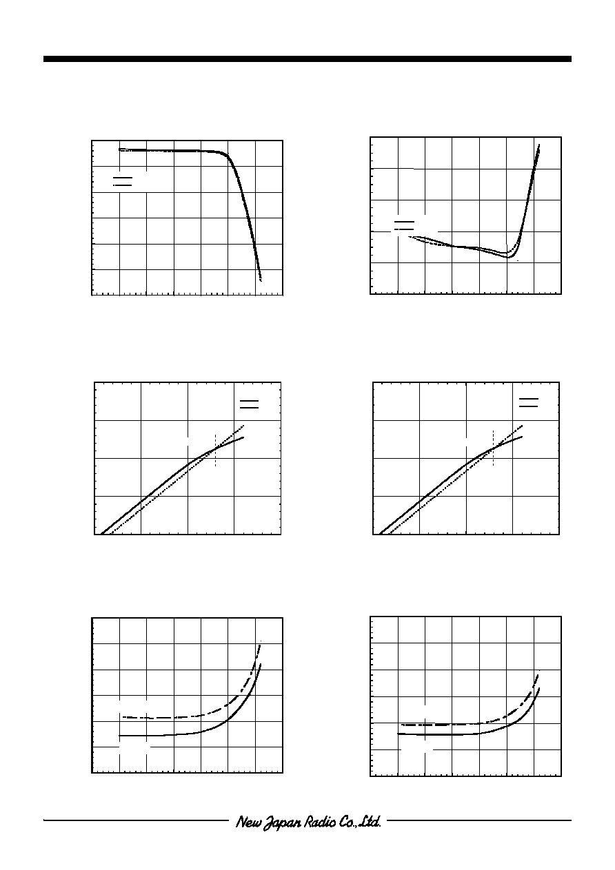
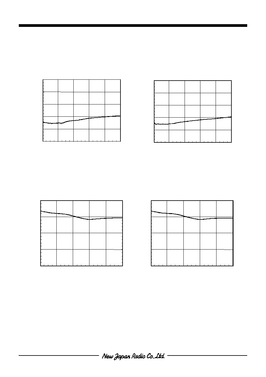
ELECTRICAL CHARACTERISTICS 1
(TEST CIRCUIT 1: V
CTR (L)
=0V, V
CTR (H)
=2.7V, Z
s
=Z
o
=50
, T
a
=25�C)
PARAMETER
SYMBOL
CONDITIONS
MIN
TYP
MAX
UNITS
Control voltage (L)
V
CTR (L)
f=0.05~2.5GHz, P
in
=10dBm
-0.2
0
0.2
V
Control voltage (H)
V
CTR (H)
f=0.05~2.5GHz, P
in
=10dBm
2.5
2.7
5.5
V
Control current
I
CTR
f=0.05~2.5GHz, P
in
=10dBm
-
2.0
4.0
uA
Isolation
ISL1
f=0.05~2.0GHz, P
in
=0dBm
43
46
-
dB
Insertion loss 1
LOSS1
f=1.0GHz, P
in
=0dBm
-
0.6
1.0
dB
Insertion loss 2
LOSS2
f=2.0GHz, P
in
=0dBm
-
0.8
1.2
dB
Pin at 1dB
compression point
P
-1dB
f=2.0GHz
19.0
22.0
-
dBm
VSWR
VSWR
f=0.05~2.5GHz, ON STATE
-
1.2
1.8
Switching time
T
SW
f=0.05~2.5GHz
-
8
-
ns
n
ELECTRICAL CHARACTERISTICS 2
(TEST CIRCUIT 2: V
CTR (L)
=0V, V
CTR (H)
=2.7V, Z
s
=Z
o
=50
, T
a
=25�C)
PARAMETER
SYMBOL
CONDITIONS
MIN
TYP
MAX
UNITS
Isolation 2
ISL2
f=1~100MHz, P
in
=0dBm
-
55
-
dB
Insertion loss 3
LOSS3
f=1~100MHz, P
in
=0dBm
-
0.5
-
dB