
NJG1515AVB2
- 1 -
TDMA ANTENNA SWITCH GaAs MMIC
n
GENERAL DESCRIPTION
n
PACKAGE OUTLINE
NJG1515AVB2 is an antenna switch IC for a digital cellular
phone of 800MHz and 1.5GHz band.
The parallel control signals of three bits connect T/R circuits
to internal two antennas or external two antennas.
The termination ports with external matching circuits make
low interference between diversity antennas.
NJG1515AVB2 features very low insertion loss and low
current consumption in a very small SSOP20 package.
n
FEATURES
l
Low voltage operation
-2.5V (Tx only) and +3.5V
l
Low current consumption
10uA typ. @P
in
=30dBm (Transmit)
2uA typ. @P
in
=10dBm (Receiving)
l
Low insertion loss
0.5dB typ. @(TX-ANT1, TX-EXT1) f=940MHz, P
in
=30dBm
0.6dB typ. @(TX-ANT1, TX-EXT1) f=1453MHz, P
in
=30dBm
l
Low Adjacent Channel
-63dBc typ. @V
DD
=+3.5V, V
SS
=-2.5V, f=940MHz, P
in
=30dBm
Leakage Power
-64dBc typ. @V
DD
=+3.5V, V
SS
=-2.5V, f=1453MHz, P
in
=30dBm
l
Package
SSOP20-B2 (Mount Size: 6.4x5.0x1.25mm)
n
PIN CONFIGURATION
NJG1515AVB2
Pin Connection
1. CTL2
2. CTL3
3. V
SS
4. EXT2
5. GND
6. EXT1
7. GND
8. TX
9. GND
10. TER2
11. ANT1
12. GND
13. RX
14. GND
15. ANT2
16. GND
17. TER1
18. GND
19. V
DD
20. CTL1
VB2 Type
(Top View)
1
2
3
4
6
7
8
9
10
5
20
19
18
17
16
15
14
13
12
11
ANT-SW
DECORDER

NJG1515AVB2
- 2 -
n
ABSOLUTE MAXIMUM RATINGS
(
T
a
=25∞C
)
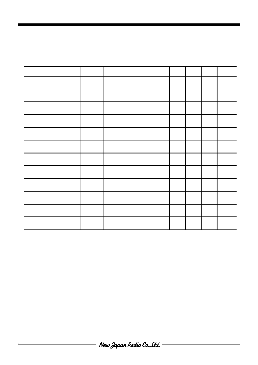
PARAMETER
SYMBOL
CONDITIONS
RATINGS
UNITS
Supply voltage 1
V
DD
V
DD
Terminal
6.0
V
Supply voltage 2
V
SS
V
SS
Terminal
-4.0
V
Control voltage
V
CTR
CTL1, CTL2, CTL3
Each Terminals
6.0
V
TX, ANT1, EXT1 Terminals
37
dBm
Input power
P
in
RX, ANT2, EXT2 Terminals
28
dBm
Power dissipation
P
D
600
mW
Operating temp.
T
opr
-40~85
∞C
Storage temp.
T
stg
-55~125
∞C
n
ELECTRICAL CHARACTERISTICS 1 [DC CHARACTERISTICS]
Common conditions: T
a
=25∞C, V
DD
=3.5V, V
SS
=-2.5V
TX, RX, ANT1, ANT2, EXT1, EXT2: terminated (50
)
TER1, TER2: connected to GND by 5pF capacitors
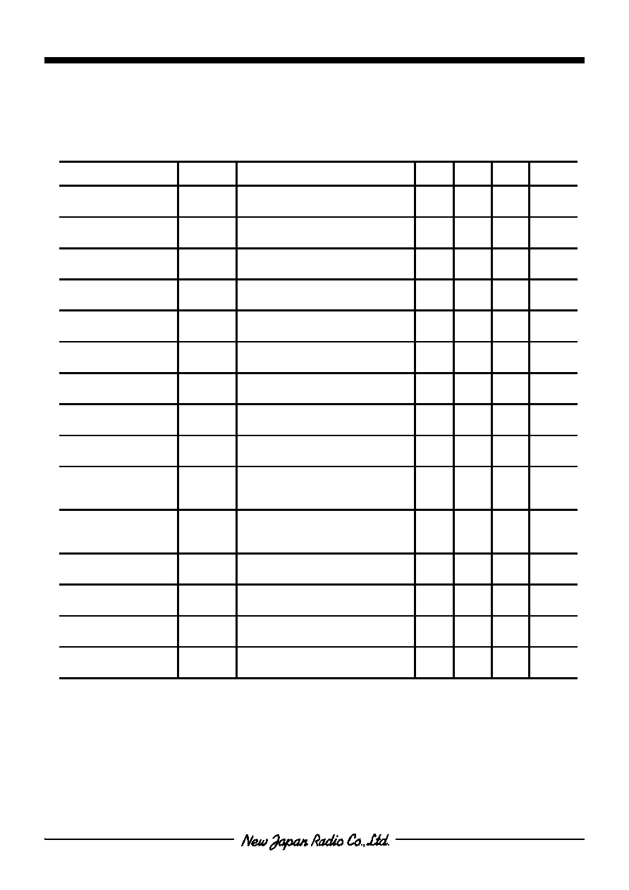
PARAMETER
SYMBOL
CONDITIONS
MIN
TYP
MAX
UNITS
Positive supply voltage
V
DD
V
DD
Terminal
2.7
3.5
5.0
V
Negative supply voltage
V
SS
V
SS
Terminal
-3.5
-2.5
-2.0
V
Current consumption 1
I
DD1
V
DD
Terminal No RF Signal
-
2.0
5.0
uA
Current consumption 2
I
SS1
V
SS
Terminal No RF Signal
-0.1
-
0
uA
Current consumption 3
I
DD2
f=0.1~2GHz, P
in
=30dBm
Transmitting state
-
10
30
uA
Current consumption 4
I
SS2
f=0.1~2GHz, P
in
=30dBm
Transmitting state
-30
-10
-
uA
Control voltage (H)
V
CTL (H)
CTL1, CTL2, CTL3 terminals
2.0
3.0
V
DD
V
Control voltage (L)
V
CTL (L)
CTL1, CTL2, CTL3 terminals
0
0
0.6
V
Control current
I
CTL
CTL1, CTL2, CTL3=VDD
or CTL1, CTL2, CTL3=0V
-1.3
-
1.3
uA
Control terminal
Input Impedance
R
in
CTL1, CTL2, CTL3
each Terminal
4
-
-
M
* The voltage of this terminal should be supplied before or same time with other DC supplying
terminals. (CTL1~3, V
SS
).

NJG1515AVB2
- 3 -
n
ELECTRICAL CHARACTERISTICS 2 [800MHz TX Mode]
Common Conditions:
PARAMETER
SYMBOL
CONDITION
MIN
TYP
MAX
UNITS
Frequency range 1
fin1
885
-
960
MHz
TX-ANT1 Insertion Loss
LOSS1
P
in
=30dBm
-
0.5
0.65
dB
TX-EXT1 Insertion Loss
LOSS2
P
in
=30dBm
-
0.5
0.65
dB
TX-RX Isolation
ISL1
P
in
=30dBm
TX-ANT1, TX-EXT1 passing
24
29
-
dB
TX-ANT1 Isolation
ISL2
P
in
=30dBm
TX-EXT1 passing
22
27
-
dB
TX-ANT2 Isolation
ISL3
P
in
=30dBm
TX-ANT1, TX-EXT1 passing
33
38
-
dB
TX-EXT1 Isolation
ISL4
P
in
=30dBm
TX-ANT1 passing
21
26
-
dB
TX-EXT2 Isolation
ISL5
P
in
=30dBm
TX-ANT1, TX-EXT1 passing
32
37
-
dB
Pin at 0.5dB
compression point 1
P
-0.5dB
(1)
TX-ANT1, TX-EXT1 passing
33
34
-
dBm
Adjacent Channel
Leakage Power 1
ACP1
PDC Standard,
±
50kHz offset
P
in
=30dBm, Input Signal
ACP=-64dBc @30dBm
-
-63
-60
dBc
Adjacent Channel
Leakage Power 3
ACP2
PDC Standard,
±
100kHz offset
P
in
=30dBm, Input Signal
ACP=-76dBc @30dBm
-
-74
-70
dBc
2nd Harmonics 1
2f0(1)
P
in
=30dBm, Input Signal 2nd
Harmonics=-68dBc
-
-63
-60
dBc
3rd Harmonics 1
3f0(1)
P
in
=30dBm, Input Signal 2nd
Harmonics=-69dBc
-
-63
-60
dBc
VSWR1
VSWR1
TX-ANT1, TX-EXT1 passing
-
1.3
1.5
Switching time
TD1
CTL1~3
-
120
500
nsec
f=960MHz, T
a
=25∞C, V
DD
=3.5V, V
SS
=-2.5V
Tested on PCB circuit as shown below.
Insertion loss of each connectors, striplines, and capacitors are excluded.
TX, RX, ANT1, ANT2, EXT1 and EXT2 are terminated to 50
.
TER1 and TER2 are connected to GND through 5pFcapacitor.
NJG1515AVB2
- 4 -
n
ELECTRICAL CHARACTERISTICS 3 [800MHz Rx Mode]
Common Conditions:
PARAMETER
SYMBOL
CONDITIONS
MIN
TYP
MAX
UNITS
Frequency range 2
fin2
810
-
885
MHz
RX-ANT1 Insertion Loss
LOSS3
P
in
=10dBm
-
0.65
0.80
dB
RX-ANT2 Insertion Loss
LOSS4
P
in
=10dBm
-
0.60
0.75
dB
RX-EXT1 Insertion Loss
LOSS5
P
in
=10dBm
-
0.70
0.85
dB
RX-EXT2 Insertion Loss
LOSS6
P
in
=10dBm
-
0.65
.80
dB
RX-ANT1 Isolation
ISL6
P
in
=10dBm, RX-ANT2,
RX-EXT1, RX-EXT2 passing
21
24
-
dB
RX-ANT2 Isolation
ISL7
P
in
=10dBm, RX-ANT1,
RX-EXT1, RX-EXT2 passing
22
25
-
dB
RX-EXT1 Isolation
ISL8
P
in
=10dBm, RX-ANT1,
RX-ANT2, RX-EXT2 passing
22
25
-
dB
RX-EXT2 Isolation
ISL9
P
in
=10dBm, RX-ANT1,
RX-ANT2, RX-EXT1 passing
20
23
-
dB
Pin at 1dB
compression point 1
P
-1
(1)
RX-ANT1, RX-ANT2,
RX-EXT1, RX-EXT2 passing
20
26
-
dBm
VSWR 2
VSWR2
RX-ANT1, RX-ANT2,
RX-EXT1, RX-EXT2 passing
-
1.4
1.6
Switching time 2
TD2
CTL1~3
-
120
500
nsec
f=885MHz, T
a
=25∞C, V
DD
=3.5V, V
SS
=0V
Tested on PCB circuit as shown below
Insertion loss of each connectors, striplines, and capacitors are excluded.
TX, RX, ANT1, ANT2, EXT1 and EXT2 are terminated to 50
.
TER1 and TER2 are connected to GND through 5pFcapacitor.
NJG1515AVB2
- 5 -
n
ELECTRICAL CHARACTERISTICS 4 [1.5GHz Tx Mode]
Common Condition:
PARAMETER
SYMBOL
CONDITIONS
MIN
TYP
MAX
UNITS
Frequency range 3
fin3
1429
-
1453
MHz
TX-ANT1
Insertion Loss
LOSS7
P
in
=30dBm
-
0.55
0.70
dB
TX-EXT1
Insertion Loss
LOSS8
P
in
=30dBm
-
0.65
0.80
dB
TX-RX Isolation
ISL10
P
in
=30dBm
TX-ANT1, TX-EXT1 passing
28
33
-
dB
TX-ANT1 Isolation
ISL11
P
in
=30dBm
TX-EXT1 passing
30
35
-
dB
TX-ANT2 Isolation
ISL12
P
in
=30dBm
TX-ANT1, TX-EXT1 passing
30
35
-
dB
TX-EXT1 Isolation
ISL13
P
in
=30dBm
TX-ANT1 passing
20
24
-
dB
TX-EXT2 Isolation
ISL14
P
in
=30dBm
TX-ANT1, TX-EXT1 passing
35
40
-
dB
Pin at 0.5dB
compression point 2
P
-0.5dB
(2) TX-ANT1, TX-EXT1 passing
33.5
35.5
-
dBm
Adjacent channel
leakage power5
ACP3
PDC Standard,
±
50KHz offset
P
in
=30dBm, Input Signal
ACP=-67dBc @ 30dBm
-
-64
-60
dBc
Adjacent channel
leakage power 7
ACP4
PDC Standard,
±
100kHz offset
P
in
=30dBm, Input Signal
ACP=-76dBc @ 30dBm
-
-75
-70
dBc
2nd Harmonics 2
2f
0
(2)
Input Signal 2nd Harmonics
=-68dBc, P
in
=30dBm
-
-62
-60
dBc
3rd Harmonics 2
3f
0
(2)
Input Signal 2nd Harmonics
=-69dBc, P
in
=30dBm
-
-62
-60
dBc
VSWR3
VSWR3
TX-ANT1, TX-EXT1 passing
-
1.4
1.6
Switching time3
TD3
CTL1~3
-
120
500
nsec
f=1453MHz, T
a
=25∞C, V
DD
=3.5V, V
SS
=-2.5V
Tested on PCB circuit as shown below
Insertion loss of each connectors, striplines, and capacitors are excluded.
TX, RX, ANT1, ANT2, EXT1 and EXT2 are terminated to 50
.
TER1 and TER2 are connected to GND through 5pFcapacitor.