Äîêóìåíòàöèÿ è îïèñàíèÿ www.docs.chipfind.ru
NJG1535HD3
- 1 -
SPDT SWITCH GaAs MMIC
s
GENERAL DESCRIPTION
s
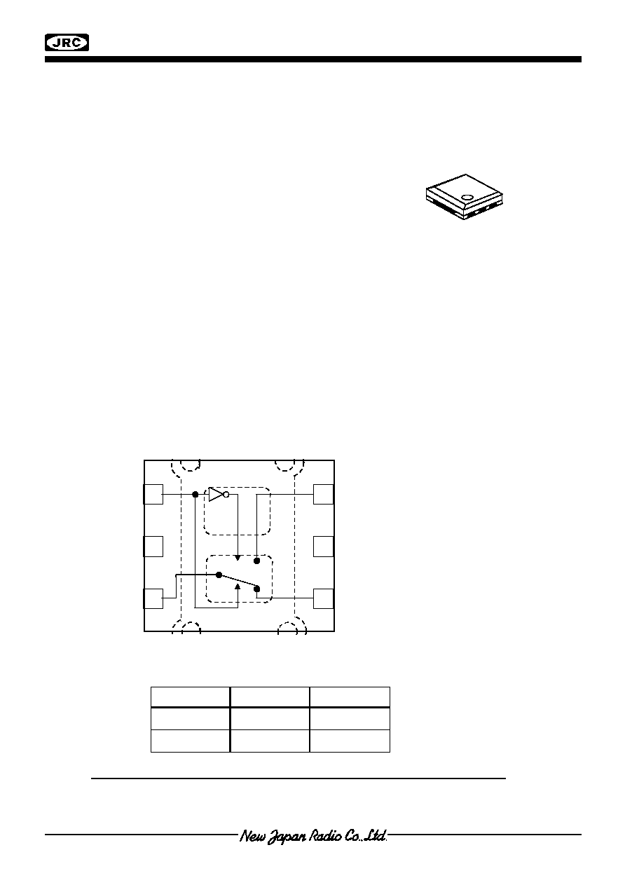
PACKAGE OUTLINE
NJG1535HD3 is a GaAs SPDT switch IC suited for
antenna switch of cellular phone handset.
This switch features high power, low loss, high isolation
and the low switch current.
This device includes logic decoder function, and can be
operated by 1 bit control signal for RF port.
The ultra small & ultra thin USB6-D3 package is adopted.
s
FEATURES
q
q
q
q
Low voltage operation
+2.5~+5.5V
q
Pin at 0.2dBcompression point
36dBm typ. @f=2GHz, V
CTL
=2.7V
q
Low insertion loss
0.3dB typ. @f=1.0GHz, P
IN
=30dBm, V
CTL
=2.7V
q
High isolation
28dB typ. @f=1.0GHz, P
IN
=30dBm, V
CTL
=2.7V
q
Low current consumption
15uA typ.
q
Ultra small & ultra thin package
USB6-D3 (Package size: 2.0x1.8x0.8mm)
s
PIN CONFIGURATION
s
TRUTH TABLE
VCTL H L
PC-P1 ON OFF
PC-P2 OFF ON
NJG1535HD3
Control Voltage: "H"=V
CTL (H)
, "L"=V
CTL (L)
Pin connection
1.VCTL
2.VDD
3.PC
4.P1
5.GND
6.P2
USB10-D3 Type
(TOP VIEW)
NOTE: Please note that any information on this catalog will be subject to change.
1
2
3
4
6
5
GND
GND
GND
GND
NJG1535HD3
- 2 -
s
ABSOLUTE MAXIMUM RATINGS
PARAMETER SYMBOL
CONDITIONS
CONDITIONS
UNITS
RF Input Power
P
IN
V
DD
=2.7V, V
CTL
=0V/2.7V 36
dBm
Supply Voltage
V
DD
VDD
terminal
7.5
V
Power Dissipation
P
D
210
mW
Control Voltage
V
CTL
VCTL
terminal
7.5
V
Operating Temp.
T
opr
-40~+85 °C
Storage Temp.
T
stg
-55~+150 °C
s
ELECTRICAL CHARACTERISTICS
(General conditions: T
a
=+25°C, Z
s
=Z
l
=50
, V
CTL (L)
=0V, V
CTL (H)
=2.7V)
PARAMETERS
SYMBOL
CONDITIONS
MIN
TYP MAX
UNITS
Supply Voltage
V
DD
2.5 2.7 5.5 V
Operating Current
I
DD
P
IN
=30dBm -
70
100
uA
Control Voltage (LOW)
V
CTL (L)
0
-
0.8
V
Control Voltage (HIGH)
V
CTL (H)
2.5
2.7
V
DD
V
Control Current
I
CTL
-
15 30 uA
Insertion Loss 1
LOSS1 f=1GHz, P
IN
=30dBm -
0.3
0.45
dB
Insertion Loss 2
LOSS2 f=2GHz, P
IN
=30dBm -
0.4
0.5
dB
Isolation 1
ISL1 f=1GHz,
P
IN
=30dBm 26
28
-
dB
Isolation 2
ISL2 f=2GHz,
P
IN
=30dBm 23
25
-
dB
Pin at 0.2dB
Compression Point
P
-0.2dB
f=2GHz
34
36
-
dBm
2nd Harmonics 1
2fo(1)
f=1GHz, P
IN
=26dBm -
-70
-65
dBc
2nd Harmonics 2
2fo(2)
f=2GHz, P
IN
=26dBm -
-75
-70
dBc
3rd Harmonics 1
3fo(1)
f=1GHz, P
IN
=26dBm -
-75
-65
dBc
3rd Harmonics 2
3fo(2)
f=1.9GHz, P
IN
=25dBm - -70
-65
dBc
Input 3
rd order
intercept Point 1
IIP3(1)
f=1000+1001MHz,
Pin=26dBm *1
58 62 - dBm
Input 3
rd order
intercept Point 2
IIP3(2)
f=2000+2001MHz,
Pin=26dBm *1
56 60 - dBm
VSWR
VSWR
f=0.1~2.5GHz, ON State
-
1.2
1.4
Switching time
T
SW
f=0.1~2GHz
-
0.8
-
us
*1: The input IP3 is defined as following equation.
IIP3=(3 x Pout - IM3) / 2 + LOSS

NJG1535HD3
- 3 -
s
TERMINAL INFORMATION
No. SYMBOL
DESCRIPTION
1 VCTL
Control signal input terminal. This terminal is set to High-Level (+2V~VDD)
or Low-Level (0~+0.8V).
2 VDD
Positive voltage supply terminal. The positive voltage (+2.5~+5.5V) have to
be supplied. Please connect a bypass capacitor with GND terminal for
excellent RF performance.
3 PC
Common RF port. The terminal PC is connected with the terminal P1 or the
terminal P2 by the voltage impressed to the terminal VCTL.
In order to block the DC bias voltage of internal circuit, an external
capacitor is required. (50~100MHz:0.01uF, 0.1~0.5GHz: 1000pF,
0.5~2.5GHz: 56pF).
4 P1
RF port. This port is connected with PC port by controlling 6th pin (V
CTL(H)
)
to 2.5~VDD. An external capacitor is required to block the DC bias voltage
of internal circuit. (50~100MHz:0.01uF, 0.1~0.5GHz: 1000pF, 0.5~2.5GHz:
56pF)
5 GND
Ground terminal. Please connect this terminal with ground plane as close
as possible for excellent RF performance.
6 P2
RF port. This port is connected with PC port by controlling 6
th
pin (V
CTL(H)
)
to 0~+0.8. An external capacitor is required to block the DC bias voltage of
internal circuit. (50~100MHz:0.01uF, 0.1~0.5GHz: 1000pF, 0.5~2.5GHz:
56pF)
NJG1535HD3
- 4 -
-2.0
-1.5
-1.0
-0.5
0.0
0.0
0.5
1.0
1.5
2.0
2.5
3.0
Ins
e
r
t
i
on Loss
(dB)
Frequency (GHz)
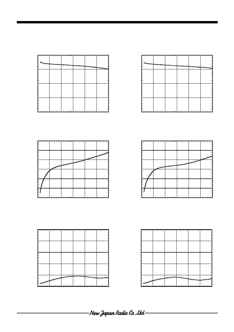
PC-P1 Insetion Loss vs. Frequency
( VDD=2.7V, VCTL=2.7V )
s
ELECTRICAL CHARACTERISTICS
(0.1~3.0GHz, with application circuit, Losses of external circuit are excluded)
-45
-40
-35
-30
-25
-20
-15
0.0
0.5
1.0
1.5
2.0
2.5
3.0
Iso
l
a
t
ion
(dB)
Frequency (GHz)
PC-P1 Isolation vs. Frequency
( VDD=2.7V, VCTL=0V )
1.0
1.2
1.4
1.6
1.8
2.0
0.0
0.5
1.0
1.5
2.0
2.5
3.0
VSWR
Frequency (GHz)
PC-P1 VSWR vs. Frequency
( VDD=2.7V, VCTL=2.7V, P1port )
-2.0
-1.5
-1.0
-0.5
0.0
0.0
0.5
1.0
1.5
2.0
2.5
3.0
Ins
e
r
t
i
on Loss
(dB)
Frequency (GHz)
PC-P2 Insetion Loss vs. Frequency
( VDD=2.7V, VCTL=0V )
-45
-40
-35
-30
-25
-20
-15
0.0
0.5
1.0
1.5
2.0
2.5
3.0
Iso
l
a
t
ion
(dB)
Frequency (GHz)
PC-P2 Isolation vs. Frequency
( VDD=2.7V, VCTL=2.7V )
1.0
1.2
1.4
1.6
1.8
2.0
0.0
0.5
1.0
1.5
2.0
2.5
3.0
VSWR
Frequency (GHz)
PC-P2 VSWR vs. Frequency
( VDD=2.7V, VCTL=0V, P2port )
NJG1535HD3
- 5 -
-1.5
-1.0
-0.5
0.0
60
100
140
180
220
260
300
26
28
30
32
34
36
38
VDD=2.5V
VDD=2.7V
VDD=5.5V
I
n
se
r
t
i
on Lo
ss
(dB)
Curre
nt
IDD (u
A)
Input Power (dBm)
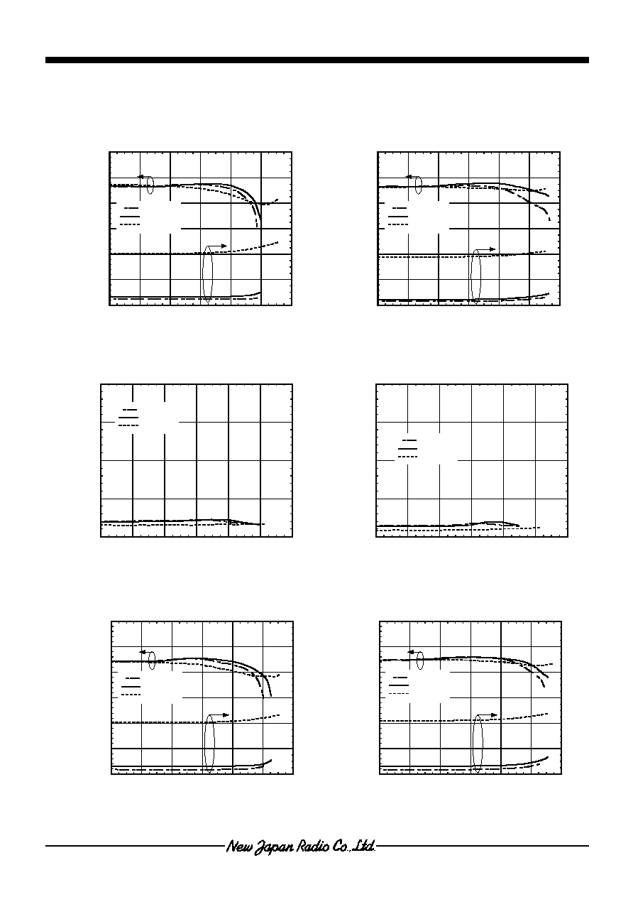
( PC-P1on, f=1GHz )
Insertion Loss, Current IDD vs. Input Power
-1.5
-1.0
-0.5
0.0
60
100
140
180
220
260
300
26
28
30
32
34
36
38
VDD=2.5V
VDD=2.7V
VDD=5.5V
I
n
se
r
t
i
on Lo
ss
(dB)
Curre
nt
IDD (u
A)
Input Power (dBm)
( PC-P1on, f=2GHz )
Insertion Loss, Current IDD vs. Input Power
s
ELECTRICAL CHARACTERISTICS
(Application circuit (Parts list 3), Losses of PCB, connector and DC blocking capacitor are included)
-30
-25
-20
-15
-10
26
28
30
32
34
36
38
VDD=2.5V
VDD=2.7V
VDD=5.5V
Isol
a
t
ion
(dB)
Input Power (dBm)
PC-P1 Isolation vs.Input Power
( PC-P2on, f=1GHz )
-30
-25
-20
-15
-10
26
28
30
32
34
36
38
VDD=2.5V
VDD=2.7V
VDD=5.5V
Isol
a
t
ion
(dB)
Input Power (dBm)
PC-P2 Isolation vs.Input Power
( PC-P1on, f=1GHz )
-1.5
-1.0
-0.5
0.0
60
100
140
180
220
260
300
26
28
30
32
34
36
38
VDD=2.5V
VDD=2.7V
VDD=5.5V
I
n
se
r
t
i
on Lo
ss
(dB)
Curre
nt
IDD (u
A)
Input Power (dBm)
( PC-P2on, f=1GHz )
Insertion Loss, Current IDD vs. Input Power
-1.5
-1.0
-0.5
0.0
60
100
140
180
220
260
300
26
28
30
32
34
36
38
VDD=2.5V
VDD=2.7V
VDD=5.5V
I
n
se
r
t
i
on Lo
ss
(dB)
Curre
nt
IDD (u
A)
Input Power (dBm)
( PC-P2on, f=2GHz )
Insertion Loss, Current IDD vs. Input Power