NJU6679
NJU6679
PRELIMINARY
PRELIMINARY
128-common x 132-segment
128-common x 132-segment
BIT MAP LCD DRIVER
BIT MAP LCD DRIVER
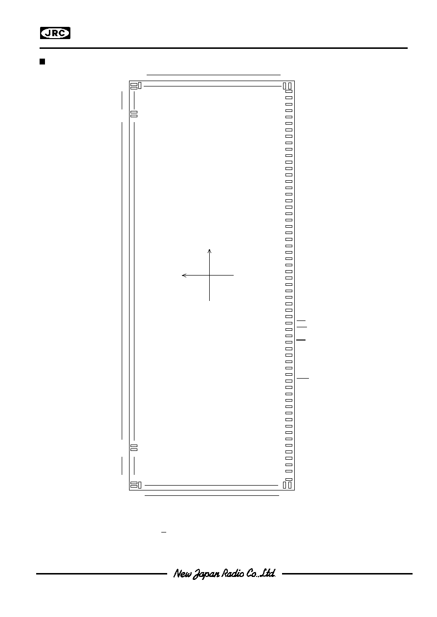
PACKAGE OUTLINE
PACKAGE OUTLINE
NJU6679CL
NJU6679CL
GENERAL DESCRIPTION
GENERAL DESCRIPTION
FEATURES
FEATURES
The NJU6679 is a bit map LCD driver to display graphics or charac-
The NJU6679 is a bit map LCD driver to display graphics or charac-
ters. It contains 25,344 bits display data RAM, microprocessor inter-
ters. It contains 25,344 bits display data RAM, microprocessor inter-
face circuits, instruction decoder, 132-segment and 128-common driv-
face circuits, instruction decoder, 132-segment and 128-common driv-
ers.
ers.
The bit image display data is transferred to the display data RAM by
The bit image display data is transferred to the display data RAM by
serial or 8-bit parallel interface.
serial or 8-bit parallel interface.
The NJU6679 displays 128 x 132 dots graphics or 8-character 8-line
The NJU6679 displays 128 x 132 dots graphics or 8-character 8-line
by 16 x 16 dots character.
by 16 x 16 dots character.
It oscillates by built-in OSC circuit without any external components.
It oscillates by built-in OSC circuit without any external components.
Furthermore, the NJU6679 features Partial Display Function which
Furthermore, the NJU6679 features Partial Display Function which
creates up to 2 blocks of active display area and optimizes duty cycle
creates up to 2 blocks of active display area and optimizes duty cycle
ratio. This function sets optimum boosted voltage by the combination
ratio. This function sets optimum boosted voltage by the combination
with both of programmable 6-time voltage booster circuit and 201-
with both of programmable 6-time voltage booster circuit and 201-
step electrical variable resistor. As result, it reduces the operating cur-
step electrical variable resistor. As result, it reduces the operating cur-
rent.
rent.
The operating voltage from 2.4V to 3.6V and low operating current are
The operating voltage from 2.4V to 3.6V and low operating current are
useful for small size battery operating items.
useful for small size battery operating items.
Direct Correspondence between Display Data RAM and LCD Pixel
Direct Correspondence between Display Data RAM and LCD Pixel
Display Data RAM - 25,344 bits (1.5 times over than display size)
Display Data RAM - 25,344 bits (1.5 times over than display size)
236 LCD Drivers - 128-common and 132-segment
236 LCD Drivers - 128-common and 132-segment
Direct Microprocessor Interface for both of 68 and 80 type MPU
Direct Microprocessor Interface for both of 68 and 80 type MPU
Serial Interface
Serial Interface
Partial Display Function
Partial Display Function
((2 blocks of active display area and automatic
2 blocks of active display area and automatic duty cycle ratio selection)
duty cycle ratio selection)
Easy Vertical Scroll by the variable start line address and over size display data RAM
Easy Vertical Scroll by the variable start line address and over size display data RAM
Programmable Bias selection ; 1/4,1/5,1/6,1/7,1/8,1/9,1/10,1/11,1/12 bias
Programmable Bias selection ; 1/4,1/5,1/6,1/7,1/8,1/9,1/10,1/11,1/12 bias
Common Driver Order Assignment by mask option
Common Driver Order Assignment by mask option
Version
Version
C
C
0
0
to C
to C
127
127
(Pin name)
(Pin name)
NJU6679A
NJU6679A Com
Com
0
0
to Com
to Com
127
127
NJU6679B
NJU6679B Com
Com
127
127
to Com
to Com
0
0
Useful Instruction Set
Useful Instruction Set
Display Data Read/Write, Display ON/OFF Cont, Inverse Display, Page Address Set,
Display Data Read/Write, Display ON/OFF Cont, Inverse Display, Page Address Set,
Display Start Line Set, Partial Display, Bias Select, Column Address Set, Status Read,
Display Start Line Set, Partial Display, Bias Select, Column Address Set, Status Read,
All On/Off, Voltage Booster Circuits Multiple Select(Maximum 6-time), n-Line Inverse,
All On/Off, Voltage Booster Circuits Multiple Select(Maximum 6-time), n-Line Inverse,
Read Modify Write, Power Saving, ADC Select, etc.
Read Modify Write, Power Saving, ADC Select, etc.
Power Supply Circuits for LCD; Programmable Voltage Booster Circuits(6-time Maximum),
Power Supply Circuits for LCD; Programmable Voltage Booster Circuits(6-time Maximum),
Regulator, Voltage Follower x 4
Regulator, Voltage Follower x 4
Precision Electrical Variable Resistance
Precision Electrical Variable Resistance
Low Power Consumption
Low Power Consumption
Operating Voltage
Operating Voltage
--- 2.4V to 3.6V
--- 2.4V to 3.6V
LCD Driving Voltage
LCD Driving Voltage --- 6.0V to 18V
--- 6.0V to 18V
Package Outline
Package Outline
--- COF / TCP / Bumped Chip
--- COF / TCP / Bumped Chip
C-MOS Technology
C-MOS Technology
JUL.10.2000
JUL.10.2000
Ver. 2.1
Ver. 2.1