
NT3882
Dot Matrix LCD 40-Channel Driver
1
V2.0 November, 1999
Features
T
Provides a 40 channel LCD driver
T
Internal serial to parallel conversion circuits:
20-bit shift register X 2
40-bit latch X 1
40-bit 4 level driver X 1
T
Logic circuit supply voltage range: 4.5V - 5.5V
T
LCD driving voltage range (V
DD
- V
EE
): 3.5V to 11V
T
Applicable LCD duty cycle: 1/2 to 1/16
T
Interfaces with a NT3881C/D LCD controller
T
LCD bias voltage can be supplied externally
T
Available in 64-pin QFP and in CHIP FORM
General Description
The NT3882 is a dot matrix LCD 40 channel driver
fabricated by low power CMOS technology. This IC
consists of two 20-bit shift registers, a 40-bit latch, and a
40-bit 4 level LCD driver. The NT3882 converts serial
data which is received from the LCD controller
(NT3881C/D) to parallel data and then outputs LCD
driving waveforms to drive LCD. Expansion of character-
type liquid crystal display can be easily obtained
according to the number and structure of characters.
Pin Configuration
Pad Configuration
1
2
3
4
5
6
7
8
9
1 0
1 1
1 2
1 3
1 4
1 5
1 6
1 7
1 8
1 9
2 0
2 1
2 2
2 3
2 4
2 5
2 6
2 7
2 8
2 9
3 0
3 1
3 2
3 3
3 4
3 5
3 6
3 7
3 8
3 9
4 0
4 1
4 2
4 3
4 4
4 5
4 6
4 7
4 8
4 9
5 0
5 1
N C
S 2 9
S 2 8
S 2 7
S 2 6
S 2 5
S 2 4
S 2 3
S 2 2
S 2 1
S 2 0
S 1 9
S 1 8
S 1 7
S 1 6
S 1 5
S 1 4
S 1 3
S 1 2
S
9
S
1
0
S
1
1
S
8
S
7
V
D
D
N
C
S
6
S
5
S
4
S
3
S
2
S
1
N C
C L 1
C L 2
G N D
D L 1
D R 1
D L 2
D R 2
N C
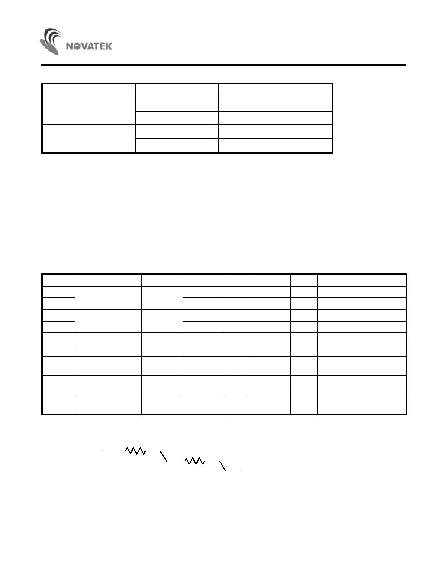
M
N C
N C
V
EE
N C
V 3
N C
N C
V 2
S
4
0
S
3
9
S
3
8
S
3
7
S
3
6
S
3
5
N
C
S
3
0
S
3
1
S
3
2
S
3
3
S
3
4
N
C
NT3882F
N C
5 2
5 3
5 4
5 5
5 6
5 7
5 8
5 9
6 0
6 1
6 2
6 3
6 4
3
4
5
6
7
8
9
1 0
1 1
1 2
1 3
1 4
1 5
1 6
1 7
1 8
2
6 3
6 2
6 1
6 0
5 9
5 7
5 6
5 5
5 4
5 3
5 2
1 9
2 0
2 1
2 2
2 3
2 4
2 7
2 8
2 9
3 0
3 1
5 1
4 8
4 6
4 2
4 0
3 9
3 8
3 7
3 6
3 5
3 4
3 2
S 2 8
S 2 7
S 2 6
S 2 5
S 2 4
S 2 3
S 2 2
S 2 1
S 2 0
S 1 9
S 1 8
S 1 7
S 1 6
S 1 5
S 1 4
S 1 3
S
1
2
S
9
S
1
0
S
1
1
S
8
S
7
V
D
D
S
6
S
5
S
4
S
3
S
2
S
4
0
S
3
9
S
3
8
S
3
7
S
3
6
S
3
5
S
3
0
S
3
1
S
3
2
S
3
3
S
3
4
S
2
9
NT3882H
2 5
S 1
C L 1
C L 2
G N D
D L 1
D R 1
D L 2
D R 2
M
V
EE
V 3
V 2

NT3882
2
Block Diagram
40-Bit 4-Level LDC Drivers
40-Bit Latch
20-Bit Shift
Register
20-Bit Shift
Register
S 1
S 2
S 1 9
S 2 0
S 2 1
S 2 2
S 3 9
S 4 0
D R 2
G N D
D L 2
D R 1
C L 2
D L 2
C L 1
M
V
E E
V
3
V
2
V
DD

NT3882
3
Pin and Pad Descriptions
Pin No.
Pad No.
Designation
I/O
External Connection
Description
2- 24,
27 - 32,
52 - 57,
59 - 63
27 - 32,
2 - 24,
52 - 57,
59 - 63
S29 - S7,
S6 - S1,
S40 - S35,
S30 - S34
O
LCD panel
Segment signal output pins
25
25
V
DD
P
Power supply
Power for logic circuits
34
34
CL1
I
Controller
Clock to latch serial data
35
35
CL2
I
Controller
Clock to shift serial data
36
36
GND
P
Power Supply
0V
37
37
DL1
I
Controlleror NT3882
Data input of 1 - 20 bits from controller
38
38
DR1
O
NT3882
Data output of 20 bit shift register
39
39
DL2
I
Controlleror NT3882
Data input of 21 - 40 bits from controller
40
40
DR2
O
NT3882
Data output of 40 bit shift register
42
42
M
I
Controller
Alternate signal for LCD drivers
46, 48, 51
46, 48, 51
V
EE
, V
3
, V
2
P
Power Supply
Power for LCD drivers
1, 26, 33, 41,
43 - 45, 47,
49, 50, 58,
64
-
NC
-
-
No connection
Functional Description
NT3882 is a dot matrix LCD segment driver LSI. It
operates with the controller, such as NT3881C/D, and/or
another segment driver LSI NT3882. NT3882 receives
serial data from the controller or another NT3882,
converts it to parallel data and then supplies the LCD
driving waveforms to the LCD panel.
1. CL1
This signal is used for latching the shift register contents.
When CL1 is set at high, the shift register contents are
transferred to the 40-bit 4level LCD driver. When CL1 is
set at low, the last display output data (S1 to S40) is
held.
2. CL2
Clock pulse inputs for the two 20-bit shift registers. The
data is shifted to a 40-bit latch at the falling edge of CL2.
The clock singal CL2 must be active when operating to
refresh shift registers' contents.
3. DL1
The 1 - 20 bit data from LCD controller is fed into the
first 20-bit shift register through DL1.
4. DR1
The 20th bit data of first 20-bit shift register output from
DR1. The data shifted out from DR1 after 20 bit delay
are synchronized with the clock pulse (CL2). By
connecting DR1 to DL2, two 20-bit shift registers can be
cascaded to one 40-bit shift register.
5. DL2
The 21 - 40 bit data from the LCD controller is fed into
the second 20-bit shift register through DL2.
6. DR2
The 40th bit data of the second 20-bit shift register
output is from DR2. The data shifted out from DR2 after
a 20-bit delay is synchronized with the clock pulse (CL2).
By connecting DR2 to the next NT3882 DL1, the cascade
construction is obtained to drive a wider LCD panel.
7. S1 to S40
These 40 bits represent the 40 data bits in the 40-bit
latch. One of V
DD
, V
2
, V
3
and V
EE
is selected as a LCD
driving voltage source according to the combination of
latched data level and the alternate signal (M).
NT3882
4
The truth table is listed as follows:
Latched Data
M
Output level of S1 to S40
1(High)
1(High)
V
EE
(Selected)
0(Low)
V
DD
0(Low)
1(High)
V
3
(Nonselected)
0(Low)
V
2
Absolute Maximum Ratings*
Power Supply Voltage (V
DD
-GND) . . . . . . . -0.3V to 7.0V
Power Supply Voltage (V
DD
-V
EE
) . . . . . . . . . . . . . . . . . .
. . . . . . . . . . . . . . . . . . . . . . . V
DD
- 13.5V to V
DD
+ 0.3V
Input Voltage . . . . . . . . . . . . . . . . . .-0.3V to V
DD
+ 0.3V
Operating Temperature . . . . . . . . . . . . . -20
q
C to + 75
q
C
Storage Temperature . . . . . . . . . . . . . .-55
q
C to + 125
q
C
*Comments
Stresses above those listed under "Absolute Maximum
Ratings" may cause permanent damage to this device.
These are stress ratings only. Functional operation of
this device at these or any other conditions above those
indicated in the operational sections of this specification
is not implied or intended. Exposed to the absolute
maximum rating conditions for extended periods may
affect device reliability.
DC Electrical Characteristics (V
DD
= 5.0V, GND = 0V, V
EE
= 0V, T
A
= 25
G
C)
Symbol
Parameter
Terminal
Min.
Typ.
Max.
Unit
Conditions
V
IH
Input Voltage
CL1, CL2
0.7 X V
DD
-
V
DD
V
V
IL
DL1, DL2
0
-
0.3 X V
DD
V
V
OH
Output Voltage
DR1, DR2
V
DD
- 0.4
-
-
V
I
OH
= -0.4mA
V
OL
-
-
0.4
V
I
OL
= 0.4mA
V
D1
Vi-Sj Voltage
Note 1
-
-
1.1
V
I
ON
= 0.1mA for one of Sj
V
D2
Descending
105
V
I
ON
= 0.05mA for each of Sj
I
IL
Input Leakage
Current
CL1, CL2
DL1, DL2
-5
-
5
P
A
V
IN
= 0 or VDD
I
VL
Vi Leakage
Current
V
2
, V
3
, V
EE
-10
-
10
P
A
S1 to S40 open
I
DD
Power Supply
Current
Note 2
-
-
200
P
A
f
CL1
= 1KH
f
CL2
= 400KHz
Note 1: V
i
- S
j
(V
i
= V
DD
, V
2
, V
3
, V
EE
; j = 1 to 40) equivalent circuit.
V
i
1Kmax.
1Kmax.
Power
Switch
Data
Swtich
S
j
Note 2: Input/output current is excluded. When the input is at the intermediate level with CMOS, some excessive current
will flow through the input circuit to the power supply. To avoid this, the input level must be fixed at a high or low
state.
NT3882
5
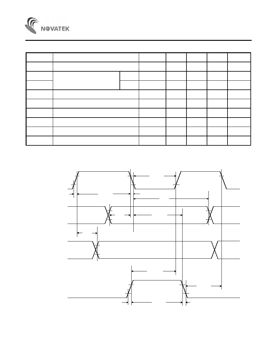
AC Characteristics
(V
DD
= 5.0V, GND = 0V, V
EE
= 0V, T
A
= 25
G
C)
Symbol
Parameter
Terminal
Min.
Typ.
Max.
Unit
f
CL2
Data Shift Frequency
CL2
-
-
400
KHz
t
CW H
Clock Width
High
CL1, CL2
800
-
-
ns
t
CW L
Low
CL2
800
-
-
ns
t
DH
Data Hold Time
DL1, DL2
300
-
-
ns
t
SUD
Data Set-up Time
DL1, DL2
300
-
-
ns
t
SUC1
Clock Set-up Time (CL2
o
CL1)
CL1, CL2
500
-
-
ns
t
SUC2
Clock Set-up Time (CL1
o
CL2)
CL1, CL2
500
-
-
ns
t
CL
Clock Rise/Fall Time
CL1, CL2
-
-
200
ns
t
PD
Data Delay Time
-
75
-
500
ns
Timing Waveforms
t
CL
V
IH
V
IL
t
CL
t
CWH
t
CWL
t
CL
t
DH
t
SUD
t
SUC1
t
PD
t
SUC2
t
SUC2
t
CWH
t
CL
V
OH
V
OL
CL2
DL1,DL2
DR1,DR2
CL1