 | –≠–ª–µ–∫—Ç—Ä–æ–Ω–Ω—ã–π –∫–æ–º–ø–æ–Ω–µ–Ω—Ç: NT6868AH | –°–∫–∞—á–∞—Ç—å:  PDF PDF  ZIP ZIP |

NT6868A
Keyboard Controller
1
V2.1
Features
n
Built-in 6502 8-bit CPU
n
2 MHz CPU operation frequency
n
4K bytes of ROM
n
128 bytes of SRAM
n
One 8-bit programmable base timer with
1 - 256
µ
sec interval
n
29 programmable bi-directional I/O pins
n
3 LED direct sink pins with internal serial resistors
n
Mask optional for built-in RC oscillator with an
external resistor or external ceramic resonator applied
n
Watch-dog timer
n
Built-in power-on reset
n
Built-in low voltage reset
n
CMOS technology for low power consumption
n
Available in 40 pin DIP package and 40 pad CHIP
FORM
General Description
NT6868A is a single chip micro-controller for keyboard
applications. It incorporates a 6502 8-bit CPU core, 4K
bytes of ROM, and 128 bytes of RAM used as working
RAM and stack area. It also includes 29 programmable
bi-directional I/O pins and one 8-bit pre-loadable base
timer. Additionally, it includes a built-in low voltage
reset, a 4MHz RC oscillator that requires only a resistor
externally applied or a 4MHz ceramic resonator, and a
watch-dog timer that prevents system standstill.
Pin Configuration
GND
NC
DATA
CLK
P30
P31
P32
P33
P34
P11
P00
P02
P03
P17
P04
P20
P21
P22
P23
P25
P26
LED0
LED1
V
DD
LED2
R/OSCO
OSCI
P12
P27
NT6868A
1
2
3
4
5
6
7
8
9
10
11
12
13
14
15
16
25
26
27
28
29
30
31
32
33
34
35
36
37
38
39
40
RESET
P01
P05
P06
P07
P10
17
18
19
20
P24
P16
P15
P14
P13
24
23
22
21
Pad Configuration
NT6868AH
16
15
14
13
12
11
10
9
8
7
6
5
4
3
2
40
39
38
37
36
35
34
33
32
31
30
29
28
27
26
25
24
23
22
21
20
19
18
17
G
N
D
N
C
D
A
T
A
C
L
K
P
3
0
R
/
O
S
C
O
V
D
D
L
E
D
2
P31
P32
P33
P34
RESET
P00
P01
P02
P03
P04
P05
P20
P21
P22
P23
P24
P25
P26
P27
LED0
LED1
P
1
7
P
1
6
P
1
5
P
1
4
P
1
3
P
1
2
P
1
1
P
1
0
P
0
7
P
0
6
1
O
S
C
I

NT6868A
2
Block Diagram
WATCH DOG
TIMER
6502
CPU
4K BYTES
ROM
128 BYTES
SRAM + STACK
BASE TIMER
INT. CONTROLLER
TIMING GENERATOR
(RC OSC/CERAMIC RESONATOR:
4MHz)
POWER-ON RESET/
LOW VOLTAGE RESET
I/O PORTS
GND
DATA
CLK
LED0
LED1
LED2
P00 - P07
P10 - P17
P30 - P34
P20 - P27
V
DD
RESET
Pin and Pad Descriptions
Pin No.
Pad No.
Designation
I/O
Description
1
1
GND
P
Ground pin
2
2
NC
-
No connection, recommended to connect V
DD
or floating
3
3
DATA
I/O
I/O, 10K
pull-up resistor for communication
4
4
CLK
I/O
I/O, 10K
pull-up resistor for communication
5 - 9,
11 - 34
5 - 9,
11 - 34
P30 - P34,
P00 - P27
I/O
Bi-directional I/O pins
10
10
RESET
I
RESET
signal input pin with internal pull up resistor; Active low
35 - 37
35 - 37
LED0 -
LED2
O
LED direct sink pins
38
38
V
DD
P
Power supply
39
39
R/OSCO
I
47K
resistor connected for RC OSC or 4MHz ceramic resonator
connected
40
40
OSCI
-
No connection for RC OSC, connected for 4MHz ceramic
resonator
* Under the constraint of the maximum frequency variation, (
F/F)
max
,
±
1%, code 3 (ceramic resonator option) must be
selected and pin 39 and pin 40 are connected to a ceramic resonator. If (
F/F)
max
,
±
10%, code 1 (RC OSC option) is
recommended to be selected and pin39 connects a 47K
resistor with,
±
1% accuracy to V
DD
and pin 40 is floating.

NT6868A
3
Functional Description
6502 CPU
6502 is an 8-bit CPU. Refer to 6502 data sheet for details.
ACCUMULATOR A
7
0
INDEX REGISTER X
7
0
INDEX REGISTER Y
7
0
PROGRAM COUNTER PC
15
0
S
7
0
7
0
S
V
B
D
I
Z
C
SIGN
OVERFOLW
BREAK
DECIMAL MODE
INTERRUPT MASK
ZERO
CARRY
STATUS REGISTER P
UNUSED
SYSTEM REGISTERS
UNUSED
USER ROM
SRAM
RST-L
IRQ-H
IRQ-L
RST-H
FFFF
FFFE
FFFD
FFFC
F000
00CF
00C0
007F
0000
STACK PTR
NMI VECTOR
IRQ VECTOR
FFFB
FFFA
NMI-L
NMI-H
STACK POINTER SP
Figure 1. 6502 CPU Registers and Status Flags
Figure 2. NT6868A Memory Map

NT6868A
4
System Reserved Registers
Address
Register
Bit7
Bit6
Bit5
Bit4
Bit3
Bit2
Bit1
Bit0
$00C0
BT
BT7
BT6
BT5
BT4
BT3
BT2
BT1
BT0
W
$00C1
TCON
-
-
-
-
-
-
-
ENBT
W
$00C2
CLRIRQX
-
-
-
-
-
-
-
CLRIRQTMR
W
$00C3
PORT0
PD07
PD06
PD05
PD04
PD03
PD02
PD01
PD00
RW
$00C4
PORT1
PD17
PD16
PD15
PD14
PD13
PD12
PD11
PD10
RW
$00C5
PORT2
PD27
PD26
PD25
PD24
PD23
PD22
PD21
PD20
RW
$00C6
PORT3
-
-
-
PD34
PD33
PD32
PD31
PD30
RW
$00C7
CLK
-
-
-
-
-
-
-
CLK
RW
$00C8
DATA
-
-
-
-
-
-
-
DATA
RW
$00C9
LED
-
-
-
-
-
LED2
LED1
LED0
W
$00CA
CLRWDT
0
1
0
1
0
1
0
1
W
$00CB
X
X
X
X
X
X
X
X
X
X
$00CC
X
X
X
X
X
X
X
X
X
X
$00CD
X
X
X
X
X
X
X
X
X
X
$00CE
X
X
X
X
X
X
X
X
X
X
$00CF
X
X
X
X
X
X
X
X
X
X
- : no effect
X : access not allowed
4K X 8 ROM
The built-in ROM program code, executed by the 6502
CPU, has a capacity of 4K X 8 bits and is addressed
from F000H to FFFFH.
128 X 8 SRAM
The built-in SRAM is used for general purpose data
memory and for the stack area. SRAM is addressed from
0000H to 007FH. User can allocate stack area in the
SRAM by setting stack pointer register (S). Because the
6502C default stack pointer is 01FFH, it must be
mapped to 007FH. Mapping from 01XX to 00XX is done
internally by setting the S register to 7FH via software
programming.
For example :
LDX #$7F
TXS
Power-On Reset
Built-in power-on reset circuit can generate a 150ms
pulse to reset the entire chip. The beginning of the
150ms pulse occurs at 60% of V
DD
when powered on.
The start of 150ms pulse
V
DD
t
power
60%
NT6868A
5
Timing Generation
This block generates the system timing and control
signal supplied to CPU and on-chip peripherals. There
are two types of system clock sources: built-in RC
oscillator or external ceramic resonator. Both of them are
mask optional and generate a 4MHz system clock. They
also generates 2MHz for CPU, and 1MHz for base timer.
The following shows the relationship of code type
number and oscillation type.
Oscillator Type
Code Number
RC OSC
1
Ceramic Resonator
3
The following table provides the relationship between
external resistor and RC OSC frequency. (for reference
only)
External Resistor
(K
)
RC OSC Frequency (MHz)
39
4.7
43
4.44
47
4
56
3.68
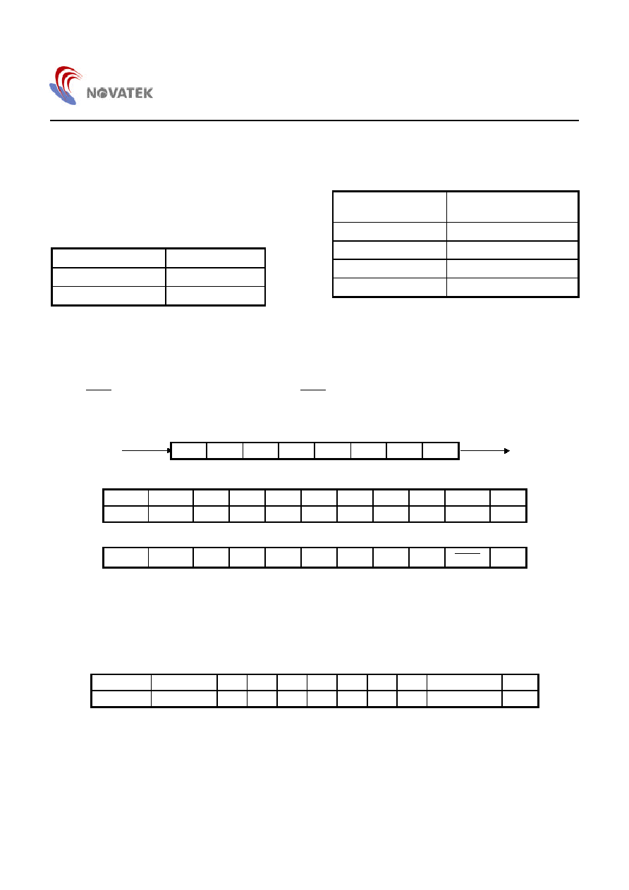
Base Timer
The base timer is an 8-bit counter with a 1MHz clock source. The base timer can be enabled/disabled by CPU. After reset,
the base timer is disabled and cleared. The base timer can be preset by writing BT7 - BT0 to the BT register at any time.
When enabled, the base timer starts counting from the preset value. When the value reaches FFH, it generates a timer
interrupt if the timer interrupt is enabled. When it reaches the maximum value of FFH, the base timer will wrap around and
begin counting at 00H. The timer interval can be programmed from 1 - 256
µ
sec. The base timer can be enabled by writing
a '0' to ' ENBT ' in the TCON (Timer Control) register. The ENBT is a level trigger.
Base timer structure:
8-Bit timer
BT7
BT6
BT5
BT4
BT2
BT2
BT1
BT0
BT pre-load data:
Addr.
Bit
7
6
5
4
3
2
1
0
$00C0
BT
BT7
BT6
BT5
BT4
BT3
BT2
BT1
BT0
(W)
Timer Control Regisrer:
$00C1
TCON
-
-
-
-
-
-
-
ENBT
(W)
INT. Controller
When BASE TIMER overflow occurs, it will set the IRQTMR flag. The IRQTMR flag cannot be directly accessed by
software. Once set by an interrupt source, it remains High unless cleared by writing '1' to the corresponding bit in
CLRIRQX ($00C2H). This register is cleared to '0' on initialization by system reset.
When an interrupt occurs, CPU jumps to $FFFEH & $FFFFH to execute the interrupt service routine. When BASE TIMER
interrupt occurs and enters the interrupt service routine, the IRQTMR flag must be cleared by software.
Interrupt Control Register:
Addr.
Bit
7
6
5
4
3
2
1
0
$00C2
CLRIRQX
-
-
-
-
-
-
-
CLRIRQTMR
(W)
1
µ
s
TMRINT