
NT68F62
8-Bit Microcontroller for Monitor (32K Flash MTP Type)
1
V1.0
Features
Operating voltage range: 4.5V to 5.5V
CMOS technology for low power consumption
6502 8-bit CMOS CPU core
8 MHz operation frequency
32K bytes of flash memory for Multi -Times Program
512 bytes of RAM
2Kbytes Masked BootROM for ISP.
One 8-bit base timer
13 channels of 8-bit PWM outputs with 5V open drain
4 channel A/D converters with 6-bit resolution
25 bi-directional I/O port pins (8 dedicated I/O pins)
Hsync/Vsync signals processor for separate &
composite signals, including hardware sync signals
polarity detection and freq. counters with 2 sets of
Hsync counting intervals
Hsync/Vsync polarity controlled output, 5 selectable
free run output signals and self-test patterns, auto-
mute function, half freq. I/O function
Two built-in IIC bus interfaces support VESA
DDC1/2B+
Two layers of interrupt management
NMI interrupt sources
- INTE0 (External INT with selectable edge trigger)
- INTMUTE (Auto Mute Activated)
IRQ interrupt sources
- INTS0/1 (SCL Go-low INT)
- INTA0/1 (Slave Address Matched INT)
- INTTX0/1 (Shift Register INT)
- INTRX0/1 (Shift Register INT)
- INTNAK0/1 (No Acknowledge)
- INTSTOP0/1 (Stop Condition Occurred INT)
- INTE1 (External INT with Selectable Edge Trigger)
- INTV (VSYNC INT)
- INTMR (Base Timer INT)
- INTADC (AD Conversion Done INT)
Hardware watch-dog timer function
40-pin P-DIP and 42-pin S-DIP packages
General Description
The NT68F62 is a new generation of monitor
�C for auto-
sync and digital control applications. Particularly, this chip
supports various functions to allow users to easily develop
USB monitors. It contains the 6502 8-bit CPU core, 512
bytes of RAM for use as working RAM and as stack area,
32K bytes of Flash memory, 13-channels of 8-bit PWM D/A
converters, 4-channel A/D converters for detection of keys
which can save I/O pins, one 8-bit pre-loadable base timer,
an internal Hsync and Vsync signals processor and a
watch-dog timer, which prevents the system from abnormal
operation and two IIC bus interfaces. The user can store
EDID data in the 128 bytes of RAM for DDC1/2B, so that
the user can reduce a dedicated EEPROM for EDID. The
half frequency output function can save the external one-
shot circuit. All of these designs are borne of our
committment to offer our user savings on component costs.
The 42 pin S-DIP IC provides two additional I/O pins �
port40 & port41, Part number NT68F62U represents the S-
DIP IC. For future reference, port40 & port42 are only
available for the 42 pin S-DIP IC.

NT68F62
2
Pin Configurations
40-Pin P-DIP
42-Pin S-DIP
[PG] DAC2
[0] DAC1/ADC3
[YE] DAC0/ADC2
[DB7] P27
[VPP] RESET
V
DD
GND
[8MHZ]OSCO
[0]OSCI
[XE] P14/PATTERN
[XA4] P12/HALFO
[XA3] P11/ADC1
[XA2] P10/ADC0
P20 [DB0]
P07/HSYNCO [XA1]
P31/SCL0 [XA7]
DAC4/SCL1 [ERASE]
DAC3 [NV]
HSYNCI[0]
VSYNCI/INTV [XA8]
NT68F62
1
2
3
4
5
6
7
8
9
10
11
12
13
14
15
16
25
26
27
28
29
30
31
32
33
34
35
36
37
38
39
40
[OE/SE] P15/INTE0
[XA5] P13/HALFI
[1]P16/INTE1
17
18
19
20
24
23
22
21
DAC5/SDA1 [MASS]
DAC6 [EXRSTB]
CREG[TMR]
P21 [DB1]
P22 [DB2]
P06/VSYNCO [XA0]
P05/DAC12 [XY5]
P04/DAC11 [XY4]
P03/DAC10 [XY3]
P02/DAC9 [XY2]
P01/DAC8 [XY1]
P00/DAC7 [XY0]
P30/SDA0 [XA6]
[DB6] P26
[DB5] P25
[DB4] P24
[DB3] P23
* [ ]: Flash Mode
P40
GND
P41
NT68F62U
1
2
3
4
5
6
7
8
9
10
11
12
13
14
15
16
27
28
29
30
31
32
33
34
35
36
37
38
39
40
41
42
17
18
19
20
21
26
25
24
23
22
[PG] DAC2
[0] DAC1/ADC3
[YE] DAC0/ADC2
[VPP] RESET
V
DD
[DB7] P27
[8MHZ]OSCO
[0]OSCI
[XE] P14/PATTERN
[XA4] P12/HALFO
[XA3] P11/ADC1
[XA2] P10/ADC0
[OE/SE] P15/INTE0
[XA5] P13/HALFI
[1]P16/INTE1
[DB6] P26
[DB5] P25
[DB4] P24
[DB3] P23
DAC4/SCL1 [ERASE]
DAC3 [NV]
HSYNCI[0]
VSYNCI/INTV [XA8]
DAC5/SDA1 [MASS]
P20 [DB0]
P07/HSYNCO [XA1]
P31/SCL0 [XA7]
DAC6 [EXRSTB]
CREG[TMR]
P21 [DB1]
P22 [DB2]
P06/VSYNCO [XA0]
P05/DAC12 [XY5]
P04/DAC11 [XY4]
P03/DAC10 [XY3]
P02/DAC9 [XY2]
P01/DAC8 [XY1]
P00/DAC7 [XY0]
P30/SDA0 [XA6]
* [ ]: Flash Mode
Block Diagram
Timing Generator
CPU core
6502
Interrupt
Controller
H/V Sync Signals
Processor
SRAM + STACK
512 Bytes
Watch Dog Timer
PWM DACs
I/O Ports
OSCI
OSCO
V
DD
GND
HSYNCI
INTE0/1
SCL0
SDA0
DAC0 - DAC7
P00 - P07
P10 - P16
P30 - P31
VSYNCO
A/D Converter
ADC0 - ADC3
8-Bit Base Timer
P40 - P41
IIC BUS
P20 - P27
HSYNCO
HALFI
HALFO
DAC8 - DAC12
VSYNCI/INTV
32KB Flash memory &
2KB BootROM
PATTERN
SCL1
SDA1
Voltage
Regulator
CREG
JEDEC Control
Block
ISP Control
Block

NT68F62
3
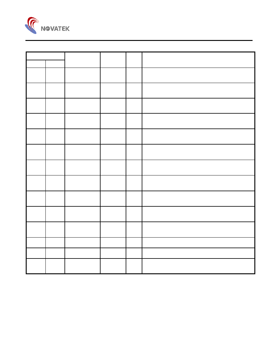
Pin Description
Pin No.
40 Pin
42 Pin
Designation Reset
Init. I/O
Description
1 1 DAC2
O
Open drain 5V, D/A converter output 2
2 2
DAC1/ADC3
DAC1
O
Open drain 5V, D/A converter output 1, shared with the A/D
converter channel 3 input
3 3
DAC0/ADC2
DAC0
O
Open drain 5V, D/A converter output 0, shared with the A/D
converter channel 2 input
4 4 RESET
I
Schmitt Trigger input pin, low active reset with internal
pulled down 50K
resistor *
5 5
V
DD
P
Power
6 7
GND
P
Ground
7
8
OSCO
O
Crystal OSC output
8
9
OSCI
I
Crystal OSC input
9 10 P15/INTE0
I/O
Bi-directional I/O pin with internal pulled up 22K
resistor,
shared with input pin of external interrupt source0 (NMI),
withSchmitt trigger, selectable triggered, and internal pulled
up 22K
resistor
10 11
P14/PATTERN I/O
Bi-directional I/O pin with internal pulled up 22K
resistor,
shared with the output of the self test pattern
11 12 P13/HALFI P13 I/O
Bi-directional I/O pin with internal pulled up 22K
resistor,
shared with the half hsync input
12 13 P12/HALFO P12 I/O
Bi-directional I/O pin with internal pulled up 22K
resistor,
shared with the half hsync output
13 14 P11/ADC1 P11 I/O
Bi-directional I/O pin with internal pulled up 22K
resistor,
shared with the A/D converter channel 1 input
14 15 P10/ADC0 P10 I/O
Bi-directional I/O pin with internal pulled up 22K
resistor,
shared with the A/D converter channel 0 input
15 16 P16/INTE1 P16 I/O
Bi-directional I/O pin with internal pulled up 22K
resistor,
shared with input pin of external interrupt source1, with
Schmitt Trigger, selectable triggered, and an internal pulled
up 22K
resistor
NT68F62
4
Pin Description (continued)
Pin No.
40 Pin
42 Pin
Designation Reset
Init. I/O
Description
16 - 23
17 - 24
P27 � P20
I/O
Bi-directional I/O pin, push-pull structure with high current
drive/sink capability
24 25 P30/SDA0 P30 I/O
Open drain 5V bi-directional I/O pin P30, shared with the
SDA0 pin of IIC bus Schmitt Trigger buffer
25 26 P31/SCL0 P31 I/O
Open drain 5V bi-directional I/O pin P31, shared with the
SCL0 pin of IIC bus Schmitt Trigger buffer
26 27 P00/DAC7 P00 I/O
Bi-directional I/O pin with internal pulled up 22K
resistor,
shared with open drain 5V D/A converter output 7
27 28 P01/DAC8 P01 I/O
Bi-directional I/O pin with internal pulled up 22K
resistor,
shared with the open drain 5V D/A converter output 8
28 29 P02/DAC9 P02 I/O
Bi-directional I/O pin with internal pulled up 22K
resistor,
shared with the open drain 5V D/A converter output 9
29 30 P03/DAC10 P03 I/O
Bi-directional I/O pin with internal pulled up 22K
resistor,
shared with the open drain 5V D/A converter output 10
30 31 P04/DAC11 P04 I/O
Bi-directional I/O pin with internal pulled up 22K
resistor,
shared with the open drain 5V D/A converter output 11
31 32 P05/DAC12 P05 I/O
Bi-directional I/O pin with internal pulled up 22K
resistor,
shared with the open drain 5V D/A converter output 12
32 33
P06/VSYNCO P06 I/O
Bi-directional I/O pin with internal pulled up 22K
resistor,
shared with the vsync out
33 34
P07/HSYNCO P07 I/O
Bi-directional I/O pin with internal pulled up 22K
resistor,
shared with the hsync out
34
35
DAC7
O
Open drain 5V, D/A converter output 7
35
36
DAC6
O
Open drain 5V, D/A converter output 6
36 38 DAC5/SDA1 DAC5 O
Open drain 5V, D/A converter output 5, shared with open
drain SDA1 line of IIC bus, Schmitt Trigger buffer
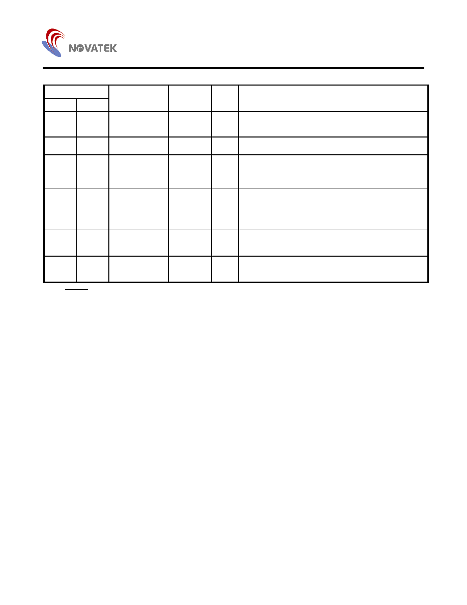
NT68F62
5
Pin Description (continued)
Pin No.
40 Pin
42 Pin
Designation Reset
Init. I/O
Description
37 39 DAC4/SCL1 DAC4 O
Open drain 5V, D/A converter output 4, shared with the
open drain SCL1 line of IIC bus, Schmitt Trigger buffer
38
40
DAC3
O
Open drain 5V, D/A converter output 3
39 41 HSYNCI
I
Debouncing & Schmitt Trigger input pin for video horizontal
sync signal, internal pull high, shared with the composite
sync input
40 42
VSYNCI/INTV
VSYNCI I
Debouncing & Schmitt trigger input pin for video vertical
sync signal, internal pull high, shared with the input pin of
the external interrupt source, intv, with Schmitt Trigger,
selectable triggered and internal pulled up 22K
resistor
- 6
P40
I/O
Bi-directional I/O pin with internal pulled up 22K
resistor,
only 42 pin S-DIP available
- 37
P41
I/O
Bi-directional I/O pin with internal pulled up 22K
resistor,
only 42 pin S-DIP available
* This RESET pin must be pulled high by an external pulled-up resistor (5K
suggestion), or it will remain at low voltage to
continually rest system.