CF1155 series
NIPPON PRECISION CIRCUITS--1
NIPPON PRECISION CIRCUITS INC.
Melody LSIs
OVERVIEW
The CF1155 series are CMOS melody LSIs that, together with a battery and piezoelectric buzzer, operate in
one of 3 melody modes determined by input level or bonding options. They also feature an oscillator stop func-
tion in non-play mode and a variable pull-down resistance function that responds to input levels in order to
reduce power consumption, reduce cost, and extend battery life, making them ideal in a wide range of applica-
tions including greeting cards and toys.
FEATURES
s
Requires few external components
s
1.2 to 3.6V wide operating voltage range
s
Low power consumption
s
3 melody modes (bonding option)
s
Oscillator stop function in non-play mode
s
Power saving pull-down resistor built-in
s
RC oscillator circuit
s
Power-ON initialization function
s
2 V
SS
pad connections
s
Wide pitch dynamic range (G
3
to D
7
)
s
Chip form
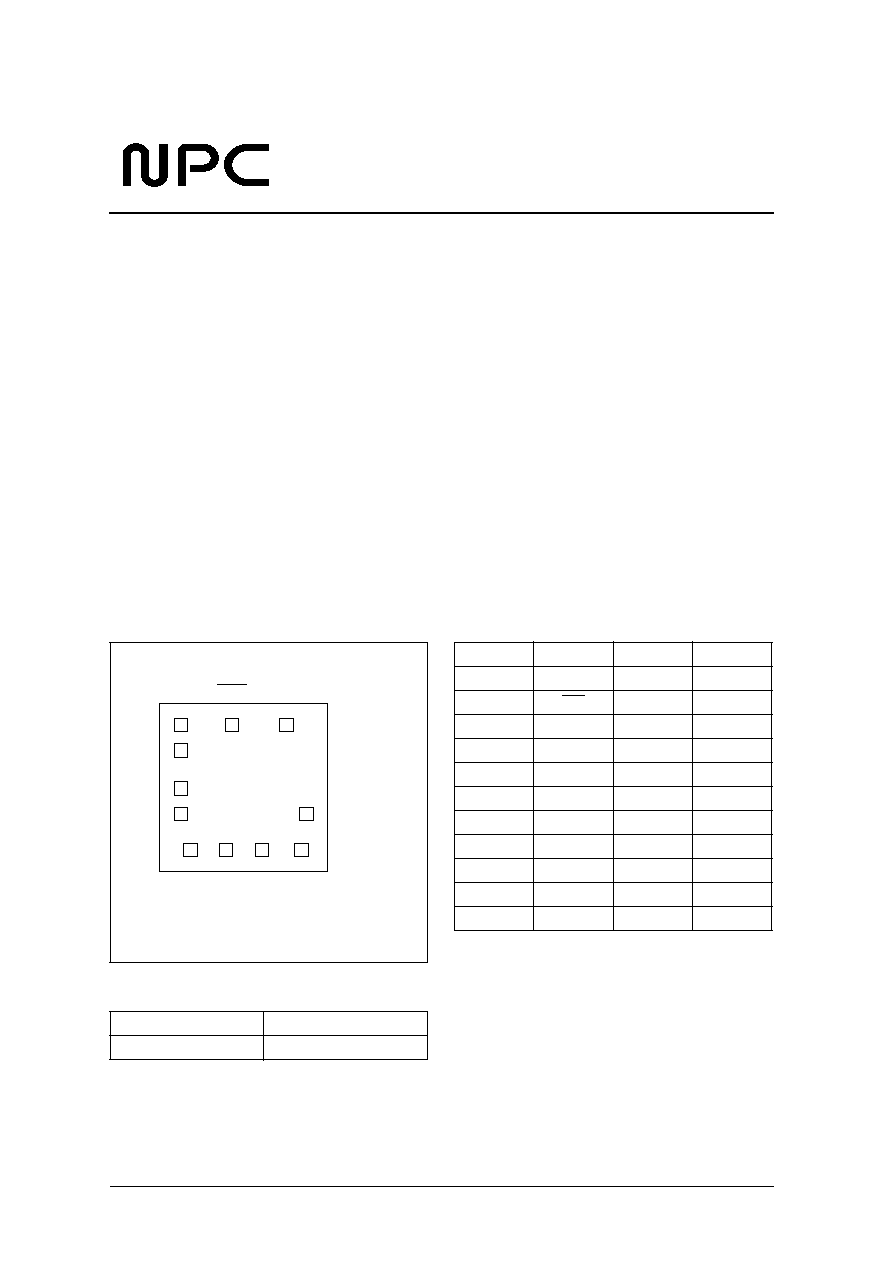
PAD LAYOUT and COORDINATES
(Unit: �m)
ORDERING INFORMATION
Chip size: 1.23
�
1 . 2 3 m m
Chip thickness: 300 � 30�m
T1, T2, T C , and TO bonding is not required.
VDD
(0,0)
(1230,1230)
1
HA1155
2
3
4
5
6
7
8
9
10
11
OUT
OUT
TC
T2
T1
VSS TO OSH
LH
VSS
N u m b e r
P a d
X
Y
1
O U T
9 3 0
1 0 7 5
2
O U T
5 2 9
1 0 7 5
3
V D D
1 5 5
1 0 7 5
4
T C
1 5 5
8 8 7
5
T 2
1 5 5
6 0 8
6
T 1
1 5 5
4 2 0
7
V S S
2 2 3
1 5 5
8
TO
4 8 6
1 5 5
9
O S H
7 5 0
1 5 5
1 0
L H
1 0 4 1
1 5 5
1 1
V S S
1 0 7 5
4 2 0
D e vice
P a ck ag e
C F 1 1 5 5
Chip form
CF1155 series
NIPPON PRECISION CIRCUITS--2
PAD DESCRIPTION
SPECIFICATIONS
Absolute Maximum Ratings
Electrical Characteristics
T
a
= 25
�
C, V
SS
= 0V, V
DD
= 1.5V
N a m e
Function
O S H , L H
Melody mode control inputs. Built-in pull-down resistors mean LOW -level signals are obtained when inputs are open circuit. The
resistance of the pull-down resistor varies with the applied voltage, as described in the Electrical Characteristics.
O U T, O U T
Piezoelectric speaker driver outputs. Both pins are LOW in non-play m o d e. OUT is LOW and O U T is HIGH during output for a
m usical rest note. Both pins are HIGH during the gap betwe e n musical notes.
V D D
Supply. The rear surface of the chip is V
D D
level.
V S S
G r o u n d
T1, T2, T C
Test inputs. Pull-down resistor built-in.
TO
Test output. The oscillator frequency (typ. 50kHz) is output for monitoring pur poses.
P arameter
S y m b o l
Condition
Rating
Unit
Supply voltage ra n g e
V
D D
-
V
S S
-
0.3 to 5.0
V
Input voltage ra n g e
V
IN
V
S S
-
0.2 to V
D D
+ 0.2
V
O p e rating temperature ra n g e
T
opr
-
20 to 80
�
C
Storage temperature ra n g e
T
stg
-
65 to 150
�
C
P arameter
S y m b o l
Condition
Rating
Unit
m i n
typ
m a x
O p e rating voltage
V
D D
1.2
1.5
3.6
V
Current consumption
1
1. Measurement circuit
I
D D 1
Non-play m o d e
�
0.01
0.3
� A
Current consumption
2
I
D D 2
Melody modes: O U T, O U T open
�
2 5
5 0
� A
L H , O S H L OW -level input voltage
V
IL
�
�
V
S S
+ 0.2
V
LH, OSH HIGH-level input voltage
V
IH
V
D D
� 0.2
�
�
V
L H , O S H L OW -level input current
I
IL
V
IL
= 0.4V
0.7
1.5
3.0
� A
LH, OSH HIGH-level input current
I
IH
V
IH
= 1.5V
0.7
1.5
3.0
� A
O U T, O U T L OW -level output current
I
O L
V
O L
= 0.75V
2.0
�
�
m A
O U T, O U T HIGH-level output current
I
O H
V
O H
= 0.75V
2.0
�
�
m A
TO oscillator frequency
f
O S C
3 5
5 0
6 5
k H z
TO frequency stability (relative to
voltage)
f/f
1
V
D D
= 1.2 to 2.0V
�
1
�
% / 0 . 1 V
f/f
2
V
D D
> 2.0V
�
2
�
% / 1 V
TO oscillator start voltage
V
D O B
�
�
1.2
V
TO oscillator stop voltage
V
D O S
�
�
1.2
V
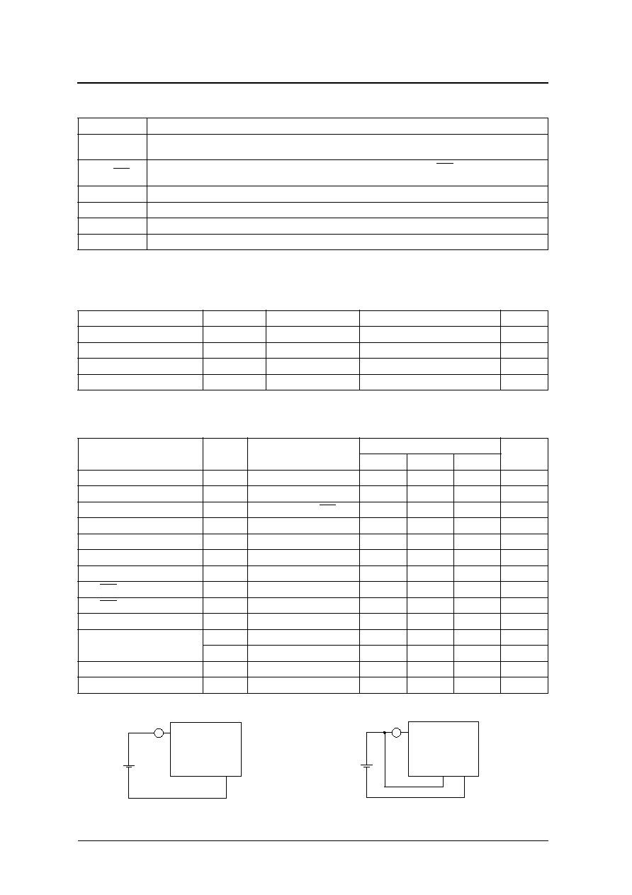
VDD
VSS
A
1.5V
2. Measurement circuit
VDD
LH
VSS
A
1.5V
CF1155 series
NIPPON PRECISION CIRCUITS--3
FUNCTIONAL DESCRIPTION
Melody Modes
The CF1155 series melody mode is determined by the bonding options and levels on the mode control inputs
OSH and LH. When either OSH or LH or both go HIGH (V
DD
), the corresponding melody mode is selected as
shown in the following table.
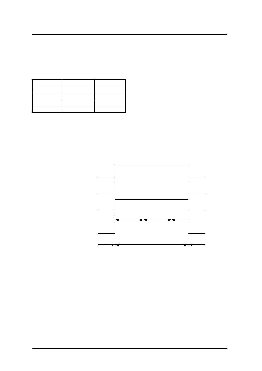
Level hold 1
When both OSH and LH go HIGH, melody play starts and continues while both are held HIGH. When both
inputs go open circuit or LOW, melody play stops, even if during mid melody.
Note that both OSH and LH inputs should be switched simultaneously using a single switch. If there is timing
difference between the two inputs, then LH has priority.
O S H
L H
M e l o d y m o d e
H I G H
H I G H
L evel hold 1
L O W
H I G H
L evel hold 2
H I G H
L O W
One-shot
L O W
L O W
Non-play
1 TUNE
Oscillator
REPEAT
REPEAT
OUT
LH
OSH
500k
135k
135k
Pull-down resistance
(2-pin parallel resistance)
CF1155 series
NIPPON PRECISION CIRCUITS--4
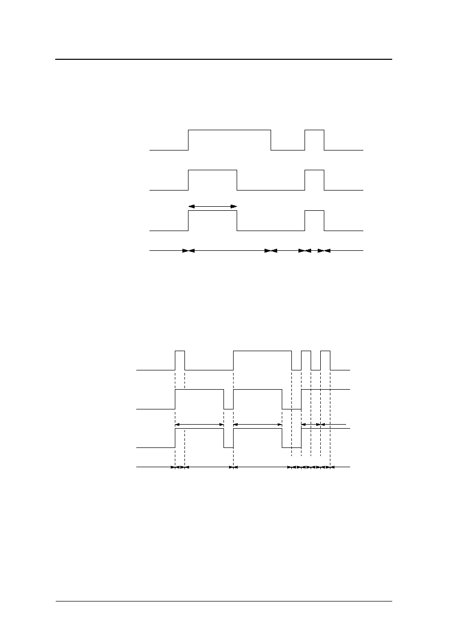
Level hold 2
When LH goes HIGH, a single melody play starts. Melody play continues until the single melody ends or LH
goes open circuit or LOW, whichever occurs first.
One-shot
When OSH goes HIGH, a single melody play starts. Melody play continues until the melody ends, even if OSH
goes open circuit or LOW mid melody. However, if the OSH input goes HIGH again during melody play, the
melody play restarts from the beginning.
1 TUNE
Oscillator
OUT
LH
1M
270k
Pull-down resistance
270k
1M
270k
1 TUNE
Oscillator
OUT
OSH
1M
270k
Pull-down resistance
270k
1M
270k
1 TUNE
1M
1M
270k
270k
From the begining

CF1155 series
NIPPON PRECISION CIRCUITS--5
Power-save Function
As shown in the preceding timing diagrams, the oscillator stops during non-play mode and the pull-down resis-
tance value changes in response to both HIGH-level and LOW-level inputs (power-save pull-down resistor) to
reduce power consumption and extend battery life.
Non-play oscillator stop function
When melody play ends, regardless of the state of either LH or OSH, the internal oscillator stops and is placed
in a standby state. In this state, the current consumption, including input pin pull-down resistor current (I
IH
max), does not exceed 3.3�A.
Power-save pull-down resistor
The resistance of the OSH and LH input pull-down resistor changes in response to the input voltage. The pull-
down resistance is 1M
when the input is HIGH, and the pull-down resistance is 270k
when the input is
LOW.
Furthermore, if a light-dependent resistor (CdS) cell is employed as a switch (the pull-down resistance is max-
imum when the CdS resistance is minimum (light) and the pull-down resistance is minimum when the CdS
resistance is maximum (dark)), the combined resistance can be increased, decreasing current consumption.
Musical Specifications
Maximum program steps
A maximum of 64 steps can be programmed into internal mask-programmable ROM. Each step represents
either a note (sound pitch and length), a rest note, or a jump. The maximum number of jumps is 7.
Note length (including rests)
Eight rhythm values, from sixteenth note to half note, for notes and rests can be programmed, as shown in the
following table.
Also, notes and rests longer than half notes and rests can be created using a tie to connect the notes. This
requires 2 program steps in ROM.
Tempo
The tempo for the standard quarter note can be selected from the following 16 options.
Pitch and scale
The CF1155 series devices support 3.5 octaves ranging from G
3
to D
7
, from which 15 notes can be selected to
form a scale.
Ty p e
C o d e
0
1
2
3
4
5
6
7
N o t e
R e s t
C o d e
0
1
2
3
4
5
6
7
8
9
A
B
C
D
E
F
=
6 9 7
3 4 8
2 3 2
1 7 4
1 3 9
1 1 6
99.4
8 7
77.3
69.6
63.3
5 8
53.5
49.7
46.4
43.5

CF1155 series
NIPPON PRECISION CIRCUITS--6
TYPICAL APPLICATION
The circuits below represent the standard connections for CF1155 series devices.
Note 1: There are 2 V
S S
pads, and either pad can be used.
Note 2: Circuit 1 is for one-shot mode, circuit 2 for level hold 1/2 modes, and circuit 3 for CdS connection.
The bonding options for the above circuits is shown in the following table.
Circuit 1
Circuit 2
OUT
VSS
VDD
OUT
OSH
LH
VSS
Piezoelectric buzzer
OUT
VSS
VDD
OUT
OSH
LH
VSS
Piezoelectric buzzer
Circuit 3
OUT
VSS
VDD
OUT
OSH
LH
VSS
Piezoelectric buzzer
Light
O S H
L H
M e l o d y m o d e
Yes
Yes
L evel hold 1
Yes
L evel hold 2
Yes
One-shot

CF1155 series
NIPPON PRECISION CIRCUITS--7
NIPPON PRECISION CIRCUITS INC. reserves the right to make changes to the products described in this data sheet in order to
improve the design or performance and to supply the best possible products. Nippon Precision Circuits Inc. assumes no responsibility fo r
the use of any circuits shown in this data sheet, conveys no license under any patent or other rights, and makes no claim that the circuits
are free from patent infringement. Applications for any devices shown in this data sheet are for illustration only and Nippon Precision
Circuits Inc. makes no claim or warranty that such applications will be suitable for the use specified without fur ther testing or modification.
The products described in this data sheet are not intended to use for the apparatus which influence human lives due to the failure or
malfunction of the products. Customers are requested to comply with applicable laws and regulations in effect now and hereinafter,
including compliance with expor t controls on the distribution or dissemination of the products. Customers shall not expor t, directly or
indirectly, any products without first obtaining required licenses and approvals from appropriate gover nment agencies.
NIPPON PRECISION CIRCUITS INC.
4-3, Fukuzumi 2-chome
Koto-ku, Tokyo 135-8430, Japan
Telephone: 03-3642-6661
Facsimile: 03-3642-6698
NC9922AE
2000.05
NIPPON PRECISION CIRCUITS INC.