CF5011 series
NIPPON PRECISION CIRCUITS INC.--1
1.8V Crystal Oscillator Module ICs
OVERVIEW
The CF5011 series are low-voltage crystal oscillator module ICs that operate at 1.8V. The crystal oscillator cir-
cuit and output buffer employ a low-voltage CMOS process operating at 1.8V. The crystal oscillator circuit has
a built-in thin-film feedback resistor with good temperature characteristics and built-in capacitors with excel-
lent frequency response, making possible a stable 3rd-harmonic oscillator with only the addition of a crystal
element.
FEATURES
I
3rd-harmonic oscillation
I
1.6 to 2.0V operating supply voltage range
I
30 to 70MHz recommended operating frequency
range
I
Inverter amplifier feedback resistor built-in
I
Oscillator capacitors C
G
, C
D
built-in
I
Standby function
I
f
O
output frequency (oscillator frequency)
I
8mA output drive capability (V
DD
= 1.6V)
I
CMOS output duty level
I
Chip form (CF5011
���
)
SERIES CONFIGURATION
Note: Recommended operating frequency is not the guaranteed value but is measured using NPC's standard crystal.
ORDERING INFORMATION
Version
Recommended
operating
frequency [MHz]
gm ratio
Built-in capacitance [pF]
R
f
[k
]
Standby function
C
G
C
D
CF5011ALA
30 to 40
1.0
14
16
4.0
Yes
CF5011ALB
1
1. Under development
40 to 50
1.0
8
16
3.9
Yes
CF5011ALC
1
50 to 60
1.0
8
16
2.2
Yes
CF5011ALD
1
60 to 70
1.5
8
16
2.7
Yes
CF5011ANA
30 to 40
1.0
14
16
4.0
No
CF5011ANB
40 to 50
1.0
8
16
3.9
No
CF5011ANC
50 to 60
1.0
8
16
2.2
No
CF5011AND
60 to 70
1.5
8
16
2.7
No
Device
Package
CF5011
���
�1
Chip form
CF5011 series
NIPPON PRECISION CIRCUITS INC.--2
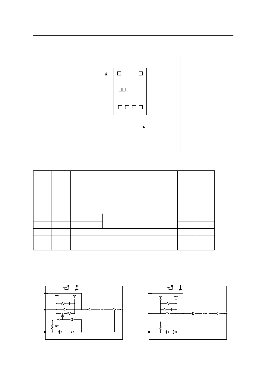
PAD LAYOUT
(Unit:
�
m)
PIN DESCRIPTION and PAD DIMENSIONS
BLOCK DIAGRAM
CF5011AL
�
CF5011AN
�
Chip size: 0.92
�
1.31 mm
Chip thickness: 300 � 30 �m
Chip base: V
DD
level
Name
I/O
Description
Pad dimensions [�m]
X
Y
INHN
I
Operation mode control input.
<CF5011AL
�
>
The oscillator stops and Q becomes high impedance when LOW. Power saving
pull-up resistor built in
<CF5011AN
�
>
Q becomes high impedance when LOW. Pull-up resistor built in
195
212
XT
I
Amplifier input
Crystal oscillator connection pins.
Crystal oscillator connected between XT and XTN
385
212
XTN
O
Amplifier output
575
212
VSS
�
Ground
766
212
Q
O
Output. Output frequency (f
O
). High impedance when INHN is LOW
765
1152
VDD
�
Supply voltage
162
1152
Q
VDD
XT
VSS
(0,0)
(920,1310)
X
Y
INHN
XTN
HA5011A
Substrate potential: V
DD
XT
VSS
VDD
Q
C
G
C
D
R
f 1
XTN
INHN
C
f
R
f 2
Substrate potential: V
DD
XT
VSS
VDD
Q
C
G
C
D
R
f 1
XTN
INHN
C
f
R
f 2
CF5011 series
NIPPON PRECISION CIRCUITS INC.--3
SPECIFICATIONS
Absolute Maximum Ratings
V
SS
= 0V
Recommended Operating Conditions
V
SS
= 0V, f
70MHz, C
L
= 15pF unless otherwise noted.
Electrical Characteristics
V
DD
= 1.6 to 2.0V, V
SS
= 0V, Ta =
-
20 to +80
�
C unless otherwise noted.
Parameter
Symbol
Condition
Rating
Unit
Supply voltage range
V
DD
-
0.5 to +3.6
V
Input voltage range
V
IN
-
0.5 to V
DD
+ 0.5
V
Output voltage range
V
OUT
-
0.5 to V
DD
+ 0.5
V
Operating temperature range
T
opr
-
40 to +85
�
C
Storage temperature range
T
stg
-
65 to +150
�
C
Output current
I
OUT
25
mA
Parameter
Symbol
Condition
Rating
Unit
min
typ
max
Supply voltage
V
DD
1.6
�
2.0
V
Input voltage
V
IN
V
SS
�
V
DD
V
Operating temperature
T
OPR
-
20
�
+80
�
C
Parameter
Symbol
Condition
Rating
Unit
min
typ
max
HIGH-level output voltage
V
OH
Q: Measurement cct 1, V
DD
= 1.6V, I
OH
= 8mA
1.1
1.3
�
V
LOW-level output voltage
V
OL
Q: Measurement cct 2, V
DD
= 1.6V, I
OL
= 8mA
�
0.3
0.4
V
Output leakage current
I
Z
Q: Measurement cct 2, INHN = LOW,
V
DD
= 2.0V
V
OH
= V
DD
�
�
10
�A
V
OL
= V
SS
�
�
10
�A
HIGH-level input voltage
V
IH
INHN
0.7V
DD
�
�
V
LOW-level input voltage
V
IL
INHN
�
�
0.3V
DD
V
Current consumption
I
DD
Measurement cct 3, load cct 1, INHN = open, C
L
= 15pF,
f = 70MHz
�
9
18
mA
Standby current
I
ST
Measurement cct 3, INHN = LOW
CF5011AL
�
�
�
100
�A
INHN pull-up resistance
R
UP1
Measurement cct 4, INHN = LOW
CF5011AL
�
0.4
�
8
M
R
UP2
Measurement cct 4, INHN = 0.7V
DD
CF5011AL
�
CF5011AN
�
50
�
150
k
AC feedback resistance
R
f1
Design value, determined by the
internal wafer pattern
CF5011ALA, ANA
3.20
4.0
4.80
k
CF5011ALB, ANB
3.12
3.9
4.68
k
CF5011ALC, ANC
1.76
2.2
2.64
k
CF5011ALD, AND
2.16
2.7
3.24
k
DC feedback resistance
R
f2
Measurement cct 5
50
�
150
k
AC feedback capacitance
C
f
Design value, determined by the internal wafer pattern
9.3
10
10.7
pF
Built-in capacitance
C
G
Design value, determined by the
internal wafer pattern
CF5011ALA, ANA
13.02
14
14.98
pF
CF5011ALB, ALC, ALD
CF5011ANB, ANC, AND
7.44
8
8.56
pF
C
D
Design value, determined by the
internal wafer pattern
CF5011ALA, ANA
14.88
16
17.12
pF
CF5011ALB, ALC, ALD
CF5011ANB, ANC, AND
14.88
16
17.12
pF
CF5011 series
NIPPON PRECISION CIRCUITS INC.--4
Switching Characteristics
V
DD
= 1.6 to 2.0V, V
SS
= 0V, Ta =
-
20 to +80
�
C unless otherwise noted.
Current consumption and Output waveform with NPC's standard crystal
FUNCTIONAL DESCRIPTION
Standby Function
Output three-state function (CF5011AL
�
, CF5011AN
�
)
When INHN goes LOW, the oscillator output on Q goes high impedance.
Oscillator stop function (CF5011AL
�
)
When INHN goes LOW, the oscillator stops.
Parameter
Symbol
Condition
Rating
Unit
min
typ
max
Output rise time
t
r
Measurement cct 3, load cct 1, 0.2V
DD
to 0.8V
DD
, C
L
= 15pF
�
1
3.5
ns
Output fall time
t
f
Measurement cct 3, load cct 1, 0.8V
DD
to 0.2V
DD
, C
L
= 15pF
�
1
3.5
ns
Output duty cycle
1
1. Monitored in sample lots.
Duty
Measurement cct 3, load cct 1, Ta = 25
�
C, V
DD
= 1.8V, C
L
= 15pF,
f
70MHz
40
�
60
%
Output disable delay time
2
2. In the case of the CF5011AL
�
, oscillator stop function is built-in. When INHN goes LOW, normal output stops. When INHN goes HIGH, normal output
is not resumed until after the oscillator start-up time has elapsed.
t
PLZ
Measurement cct 3, load cct 1, Ta = 25
�
C, V
DD
= 1.6V, C
L
15pF
�
�
100
ns
Output enable delay time
2
t
PZL
�
�
100
ns
Version
INHN
Q
Oscillator
CF5011AL
�
HIGH (or open)
f
O
output frequency
Normal operation
LOW
High impedance
Stop
CF5011AN
�
HIGH (or open)
f
O
output frequency
Normal operation
LOW
High impedance
Normal operation
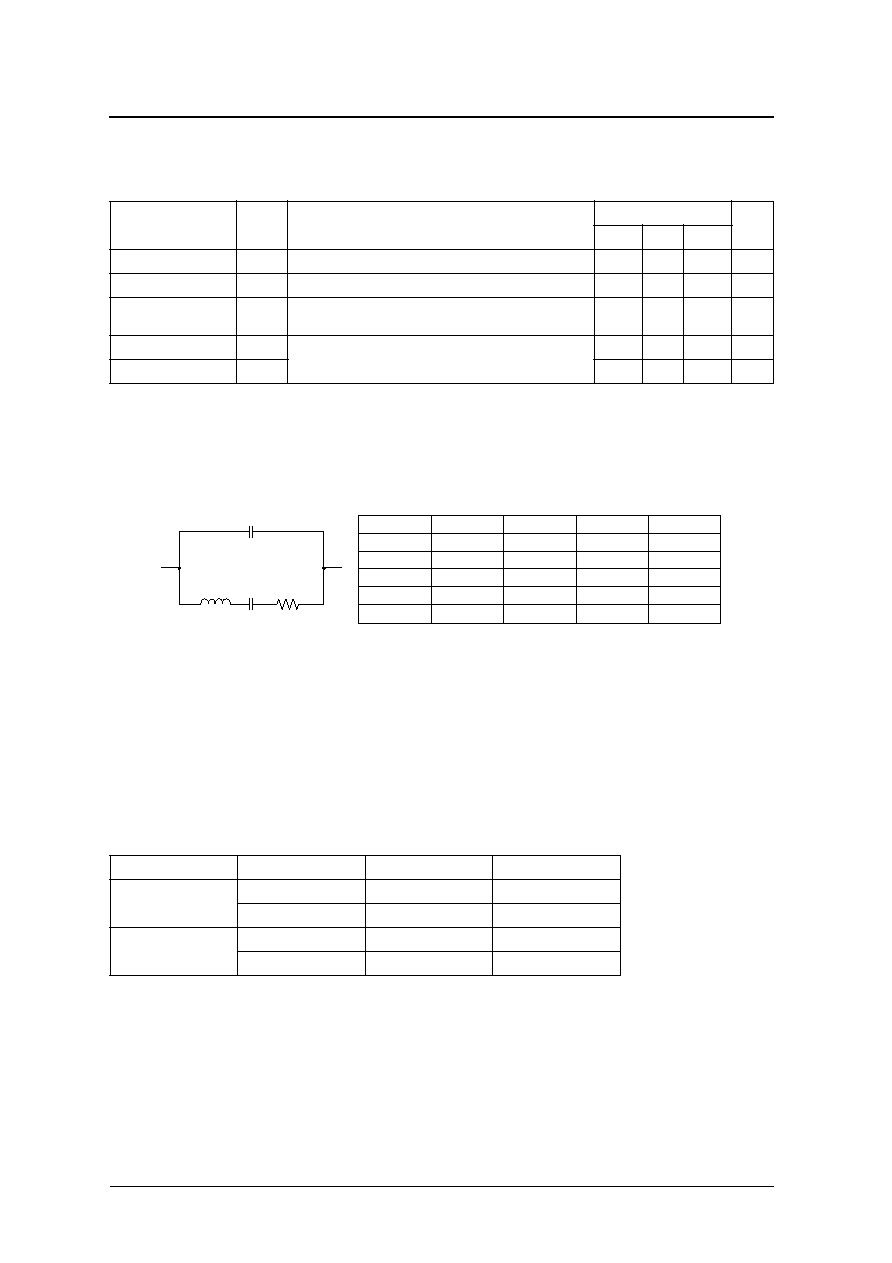
f (MHz)
R (
)
L (mH)
Ca (fF)
Cb (pF)
30
18.62
16.24
1.733
5.337
40
20.53
11.34
1.396
3.989
50
22.17
7.40
1.370
4.105
60
15.37
3.83
1.836
5.191
70
25.42
4.18
1.254
5.170
L
Ca
R
Cb

CF5011 series
NIPPON PRECISION CIRCUITS INC.--5
MEASUREMENT CIRCUITS
Measurement cct 1
1.0V
P
-P
, 10MHz sine wave input signal
C1 : 0.001
�F
R1 : 50
R2 : 137.5
Measurement cct 4
Measurement cct 2
Measurement cct 5
Measurement cct 3
Load cct 1
C
L
= 15pF
Signal
Generator
VDD
VSS
XT
Q
R1
R2
C1
V
OH
0V
Q output
INHN
XTN
VDD
VSS
I
PR
INHN
A
R
UP1
=
V
DD
I
PR
(V
PR
= V
SS
)
R
UP2
=
I
PR
(V
PR
= 0.7V
DD
)
XT
X'tal
XTN
V
PR
V
V
DD
V
PR
Q
VDD
VSS
Q
V
OL
V
A
I
OL
, I
Z
I
Z
INHN
XT
XTN
VDD
VSS
I
Rf
R
f2
=
XT
V
DD
I
Rf
XTN
A
INHN
VDD
VSS
XT
Q
X'tal
XTN
INHN
I
DD
A
Q output
C
L
(Including probe capacitance)