CF5020 series
NIPPON PRECISION CIRCUITS INC.--1
High-Frequency, 3rd Overtone Crystal Oscillator Module ICs
OVERVIEW
The CF5020 series are high-frequency, 3rd overtone crystal oscillator module ICs. They incorporate an oscilla-
tor circuit and an output buffer that operate at high frequency on a single chip. The oscillator circuit employs
CMOS inverters and a built-in damping resistor R
D
, reducing the crystal current compared with existing
devices. The damping resistor R
D
is fabricated using NPC's unique high-precision thin-film resistor technol-
ogy, which suppresses oscillator characteristic variations due to changes in temperature and voltage to a mini-
mum. The CF5020 series can be utilized to construct stable, high-frequency, 3rd overtone crystal oscillators.
FEATURES
I
R
D
built-in to reduce crystal current in the oscilla-
tor circuit
I
2.25 to 3.6V operating supply voltage range
I
Recommended operating frequency range
(varies with version)
� 2.5V operation: 60 to 155MHz
� 3.0V operation: 60 to 170MHz
I
� 40 to 85
�
C operating temperature range
I
Oscillator capacitors with excellent frequency
response built-in
I
Feedback resistors with good temperature charac-
teristics built-in
I
Standby function
� High impedance in standby mode, oscillator stops
I
Low standby current
� Power-saving pull-up resistor built-in
I
Oscillation detector function
I
CMOS output duty level (1/2VDD)
I
50
�
5% output duty (at 1/2VDD)
I
30pF output load (3.3V operation)
I
Molybdenum-gate CMOS process
I
Chip form (CF5020AL
�
)
APPLICATIONS
I
Crystal oscillator modules (3rd overtone oscillation)
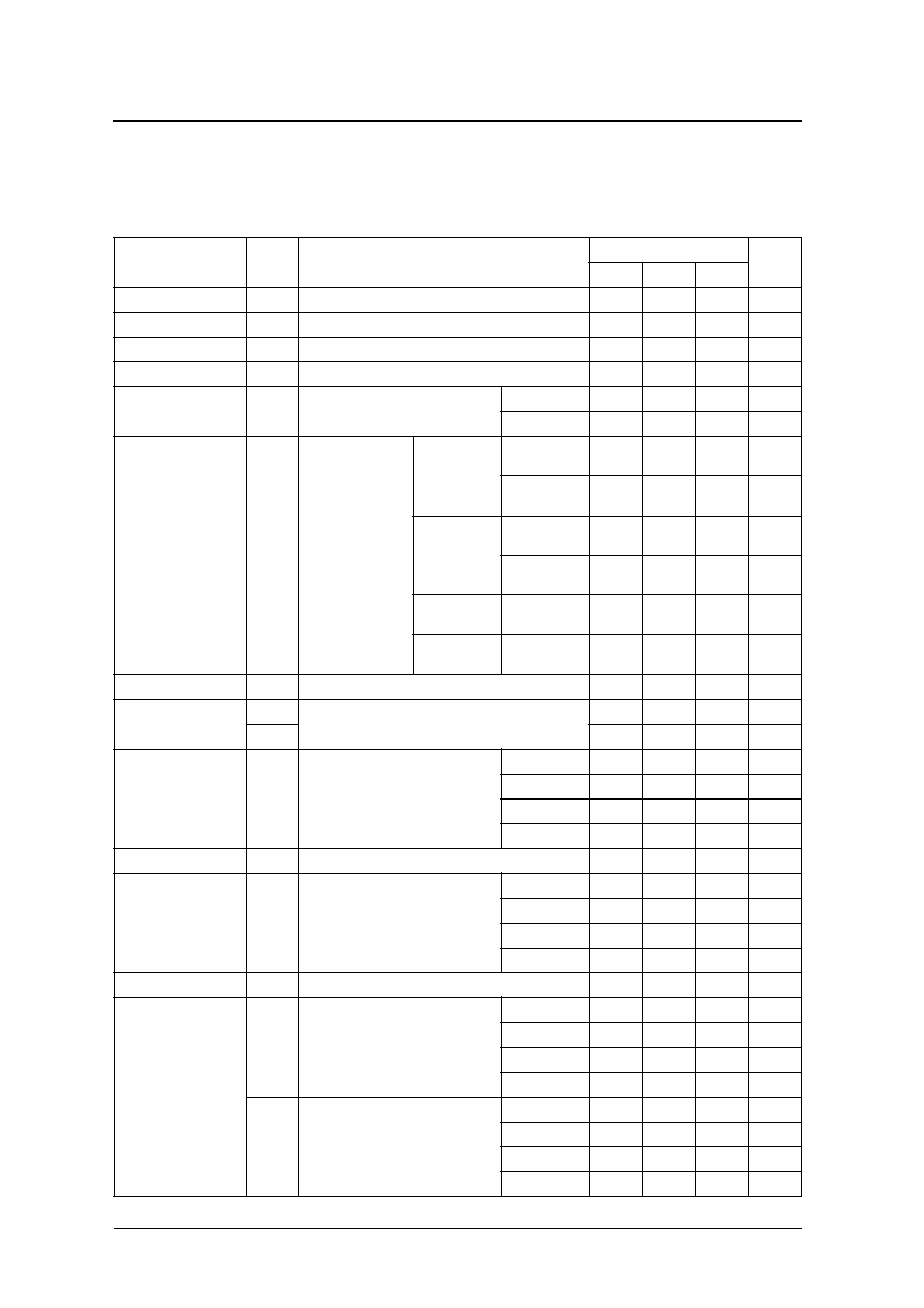
SERIES CONFIGURATION
ORDERING INFORMATION
Version
Recommended operating
frequency range
*1
[MHz]
*1. The recommended operating frequency is a yardstick value derived from the crystal used for NPC characteristics authentication. However, the oscilla-
tor frequency band is not guaranteed. Specifically, the characteristics can vary greatly due to crystal characteristics and mounting conditions, so the
oscillation characteristics of components must be carefully evaluated.
Oscillator circuit constants
INHN
input
level
Standby mode
gm ratio
Built-in capacitance Feedback
resistance
Rf [k
]
Damping
resistance
R
D
[
]
Oscillator
stop
function
Output
state
2.5V operation 3.0V operation
C
G
[pF]
C
D
[pF]
CF5020ALA
60 to 80
60 to 90
0.6
4
7
2.5
200
CMOS
Yes
High
impedance
CF5020ALB
70 to 115
80 to 125
0.8
3
3
4.5
57
CF5020ALC
105 to 135
115 to 145
1.0
1
3
3.3
57
CF5020ALD
110 to 155
135 to 170
1.0
1
5
2.2
57
Device
Package
CF5020AL
�
�2
Chip form
CF5020 series
NIPPON PRECISION CIRCUITS INC.--2
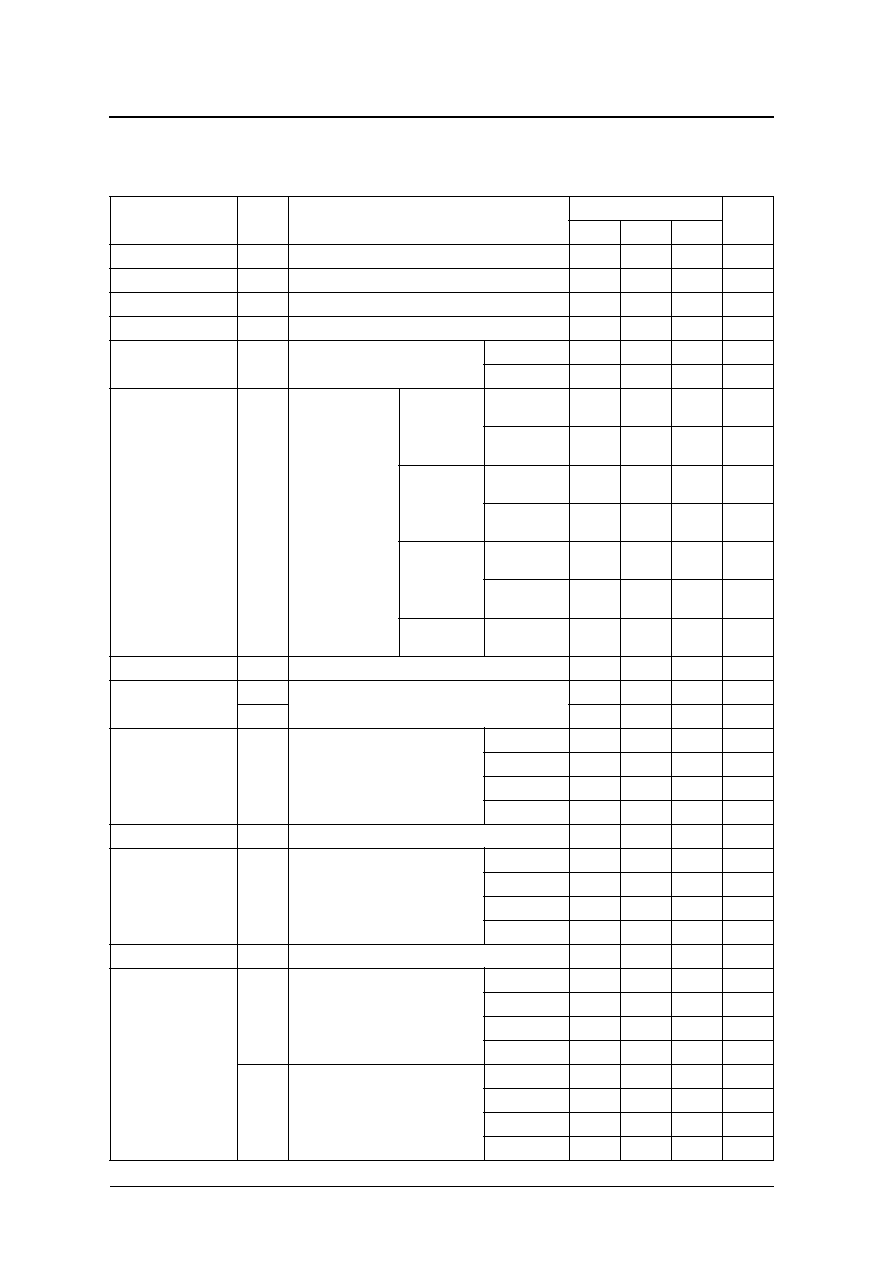
PAD LAYOUT
(Unit:
�
m)
PIN DESCRIPTION and PAD DIMENSIONS
BLOCK DIAGRAM
Chip size: 0.9
�
1.05mm
Chip thickness: 220�m � 30�m
PAD size: 90�m
Chip base: V
DD
level
Name
I/O
Description
Pad dimensions [�m]
X
Y
INHN
I
Output state control input. High impedance when LOW (oscillator stops).
Power-saving pull-up resistor built-in.
144.6
190.6
XT
I
Amplifier input
Crystal connection pins.
Crystal is connected between XT and XTN.
347.8
171
XTN
O
Amplifier output
560.6
171
VSS
�
(�) ground
755.4
497.8
Q
O
Output
755.4
905.4
VDD
�
(+) supply voltage
151.4
918.2
INHN = LOW active
Q
VDD
XTN
VSS
(0,0)
(900,1050)
X
Y
HA5020
INHN
XT
NPC
XT
VSS
VDD
Q
C
G
C
D
R
f 1
XTN
INHN
R
f 2
C
f
R
D
CF5020 series
NIPPON PRECISION CIRCUITS INC.--3
SPECIFICATIONS
Absolute Maximum Ratings
V
SS
= 0V
Recommended Operating Conditions
CF5020ALA, CF5020ALB
3V Operation
V
SS
= 0V
2.5V Operation
V
SS
= 0V
Parameter
Symbol
Condition
Rating
Unit
Supply voltage range
V
DD
-
0.5 to +7.0
V
Input voltage range
V
IN
-
0.5 to V
DD
+ 0.5
V
Output voltage range
V
OUT
-
0.5 to V
DD
+ 0.5
V
Operating temperature range
T
opr
-
40 to +85
�
C
Storage temperature range
T
STG
-
65 to +150
�
C
Output current
I
OUT
25
mA
Parameter
Symbol
Condition
Rating
Unit
min
typ
max
Operating supply voltage range
V
DD
f
125MHz
C
L
15pF
2.7
�
3.6
V
C
L
30pF
3.0
�
3.6
V
2.7
*1
*1. The output duty cycle variability increases than other conditions.
�
3.6
*1
V
Input voltage range
V
IN
V
SS
�
V
DD
V
Operating temperature range
T
OPR
-
40
�
+85
�
C
Parameter
Symbol
Condition
Rating
Unit
min
typ
max
Operating supply voltage range
V
DD
f
106MHz
C
L
15pF
2.25
�
2.75
V
f
70MHz
C
L
30pF
2.25
�
2.75
V
f
125MHz
C
L
15pF
2.25
*1
*1. The output duty cycle variability increases than other conditions.
�
2.75
*1
V
Input voltage range
V
IN
V
SS
�
V
DD
V
Operating temperature range
T
OPR
-
40
�
+85
�
C
CF5020 series
NIPPON PRECISION CIRCUITS INC.--4
CF5020ALC, CF5020ALD
3V Operation
V
SS
= 0V
2.5V Operation
V
SS
= 0V
Parameter
Symbol
Condition
Rating
Unit
min
typ
max
Operating supply voltage range
V
DD
f
170MHz
C
L
15pF
2.7
�
3.6
V
f
125MHz
C
L
30pF
2.7
�
3.6
V
Input voltage range
V
IN
V
SS
�
V
DD
V
Operating temperature range
T
OPR
-
40
�
+85
�
C
Parameter
Symbol
Condition
Rating
Unit
min
typ
max
Operating supply voltage range
V
DD
f
155MHz
C
L
15pF
2.25
�
2.75
V
Input voltage range
V
IN
V
SS
�
V
DD
V
Operating temperature range
T
OPR
-
40
�
+85
�
C
CF5020 series
NIPPON PRECISION CIRCUITS INC.--5
Electrical Characteristics
2.5V operation
V
DD
= 2.25 to 2.75V, V
SS
= 0V, Ta =
-
40 to +85
�
C unless otherwise noted.
Parameter
Symbol
Condition
Rating
Unit
min
typ
max
HIGH-level output voltage
V
OH
Q: Measurement cct 1, V
DD
= 2.25V, I
OH
= 8mA
1.75
1.95
�
V
LOW-level output voltage
V
OL
Q: Measurement cct 2, V
DD
= 2.25V, I
OL
= 8mA
�
0.3
0.4
V
HIGH-level input voltage
V
IH
INHN
0.7V
DD
�
�
V
LOW-level input voltage
V
IL
INHN
�
�
0.3V
DD
V
Output leakage current
I
Z
Q: Measurement cct 2, INHN = LOW
V
OH
= V
DD
�
�
10
�A
V
OL
= V
SS
�
�
10
�A
Current consumption
I
DD
Measurement cct 3,
load cct 1,
INHN = open
CF5020ALA
C
L
= 15pF
f = 80MHz
�
15
40
mA
C
L
= 30pF
f = 70MHz
�
20
50
mA
CF5020ALB
C
L
= 15pF
f = 106MHz
�
20
50
mA
C
L
= 30pF
f = 70MHz
�
20
50
mA
CF5020ALC
C
L
= 15pF
f = 135MHz
�
25
60
mA
CF5020ALD
C
L
= 15pF
f = 155MHz
�
30
70
mA
Standby current
I
ST
Measurement cct 3, INHN = LOW
�
�
3
�A
INHN pull-up resistance
R
UP1
Measurement cct 4
2
6
12
M
R
UP2
50
100
150
k
AC feedback resistance
R
f1
Design value.
A monitor pattern on a wafer is tested.
CF5020ALA
2.12
2.5
2.88
k
CF5020ALB
3.82
4.5
5.18
k
CF5020ALC
2.80
3.3
3.80
k
CF5020ALD
1.87
2.2
2.53
k
DC feedback resistance
R
f2
Measurement cct 5
50
100
150
k
Oscillator amplifier output
resistance
R
D
Design value.
A monitor pattern on a wafer is tested.
CF5020ALA
170
200
230
CF5020ALB
48.4
57
65.6
CF5020ALC
48.4
57
65.6
CF5020ALD
48.4
57
65.6
AC feedback capacitance
C
f
Design value. A monitor pattern on a wafer is tested.
8.5
10
11.5
pF
Built-in capacitance
C
G
Design value.
A monitor pattern on a wafer is tested.
CF5020ALA
3.40
4
4.60
pF
CF5020ALB
2.55
3
3.45
pF
CF5020ALC
0.85
1
1.15
pF
CF5020ALD
0.85
1
1.15
pF
C
D
Design value.
A monitor pattern on a wafer is tested.
CF5020ALA
5.95
7
8.05
pF
CF5020ALB
2.55
3
3.45
pF
CF5020ALC
2.55
3
3.45
pF
CF5020ALD
4.25
5
5.75
pF
CF5020 series
NIPPON PRECISION CIRCUITS INC.--6
3V operation
V
DD
= 2.7 to 3.6V, V
SS
= 0V, Ta =
-40 to +85�C unless otherwise noted.
Parameter
Symbol
Condition
Rating
Unit
min
typ
max
HIGH-level output voltage
V
OH
Q: Measurement cct 1, V
DD
= 2.7V, I
OH
= 8mA
2.2
2.4
�
V
LOW-level output voltage
V
OL
Q: Measurement cct 2, V
DD
= 2.7V, I
OL
= 8mA
�
0.3
0.4
V
HIGH-level input voltage
V
IH
INHN
0.7V
DD
�
�
V
LOW-level input voltage
V
IL
INHN
�
�
0.3V
DD
V
Output leakage current
I
Z
Q: Measurement cct 2, INHN = LOW
V
OH
= V
DD
�
�
10
�A
V
OL
= V
SS
�
�
10
�A
Current consumption
I
DD
Measurement cct 3,
load cct 1,
INHN = open
CF5020ALA
C
L
= 15pF
f = 90MHz
�
20
50
mA
C
L
= 30pF
f = 90MHz
�
25
60
mA
CF5020ALB
C
L
= 15pF
f = 125MHz
�
25
60
mA
C
L
= 30pF
f = 125MHz
�
40
100
mA
CF5020ALC
C
L
= 15pF
f = 135MHz
�
30
70
mA
C
L
= 30pF
f = 125MHz
�
40
100
mA
CF5020ALD
C
L
= 15pF
f = 170MHz
�
40
100
mA
Standby current
I
ST
Measurement cct 3, INHN = LOW
�
�
5
�A
INHN pull-up resistance
R
UP1
Measurement cct 4
2
4
8
M
R
UP2
50
100
150
k
AC feedback resistance
R
f1
Design value.
A monitor pattern on a wafer is tested.
CF5020ALA
2.12
2.5
2.88
k
CF5020ALB
3.82
4.5
5.18
k
CF5020ALC
2.80
3.3
3.80
k
CF5020ALD
1.87
2.2
2.53
k
DC feedback resistance
R
f2
Measurement cct 5
50
100
150
k
Oscillator amplifier output
resistance
R
D
Design value.
A monitor pattern on a wafer is tested.
CF5020ALA
170
200
230
CF5020ALB
48.4
57
65.6
CF5020ALC
48.4
57
65.6
CF5020ALD
48.4
57
65.6
AC feedback capacitance
C
f
Design value. A monitor pattern on a wafer is tested.
8.5
10
11.5
pF
Built-in capacitance
C
G
Design value.
A monitor pattern on a wafer is tested.
CF5020ALA
3.40
4
4.60
pF
CF5020ALB
2.55
3
3.45
pF
CF5020ALC
0.85
1
1.15
pF
CF5020ALD
0.85
1
1.15
pF
C
D
Design value.
A monitor pattern on a wafer is tested.
CF5020ALA
5.95
7
8.05
pF
CF5020ALB
2.55
3
3.45
pF
CF5020ALC
2.55
3
3.45
pF
CF5020ALD
4.25
5
5.75
pF
CF5020 series
NIPPON PRECISION CIRCUITS INC.--7
Switching Characteristics
CF5020ALA, CF5020ALB
2.5V operation
V
DD
= 2.25 to 2.75V, V
SS
= 0V, Ta =
-40 to +85�C unless otherwise noted.
3V operation
V
DD
= 2.7 to 3.6V, V
SS
= 0V, Ta =
-40 to +85�C unless otherwise noted.
Parameter
Symbol
Condition
Rating
Unit
min
typ
max
Output rise time
t
r1
Measurement cct 3, load cct 1,
0.1V
DD
to 0.9V
DD
C
L
= 15pF
�
1
3
ns
t
r2
C
L
= 30pF
�
2
5.5
ns
Output fall time
t
f1
Measurement cct 3, load cct 1,
0.9V
DD
to 0.1V
DD
C
L
= 15pF
�
1
3
ns
t
f2
C
L
= 30pF
�
2
5.5
ns
Output duty cycle
*1
*1. The duty cycle characteristic is checked the sample chips of each production lot.
Duty1
Measurement cct 3, load cct 1,
V
DD
= 2.5V, Ta = 25
�C
C
L
= 15pF, f = 106MHz
45
�
55
%
C
L
= 15pF, f = 125MHz
40
�
60
%
Duty2
C
L
= 30pF, f = 70MHz
45
�
55
%
Output disable delay time
*2
*2. Oscillator stop function is built-in. When INHN goes LOW, normal output stops. When INHN goes HIGH, normal output is not resumed until after the
oscillator start-up time has elapsed.
t
PLZ
Measurement cct 6, load cct 1, V
DD
= 2.5V, Ta = 25
�C,
C
L
= 15pF
�
�
100
ns
Output enable delay time
*2
t
PZL
�
�
100
ns
Parameter
Symbol
Condition
Rating
Unit
min
typ
max
Output rise time
t
r1
Measurement cct 3, load cct 1,
0.1V
DD
to 0.9V
DD
C
L
= 15pF
�
1
2.5
ns
t
r2
V
DD
= 3.0 to 3.6V
C
L
= 30pF
�
1.5
3
ns
Output fall time
t
f1
Measurement cct 3, load cct 1,
0.9V
DD
to 0.1V
DD
C
L
= 15pF
�
1
2.5
ns
t
f2
V
DD
= 3.0 to 3.6V
C
L
= 30pF
�
1.5
3
ns
Output duty cycle
*1
*1. The duty cycle characteristic is checked the sample chips of each production lot.
Duty2
Measurement cct 3, load cct 1, V
DD
= 3.0V, Ta = 25
�C,
C
L
= 30pF, f = 125MHz
45
�
55
%
Output disable delay time
*2
*2. Oscillator stop function is built-in. When INHN goes LOW, normal output stops. When INHN goes HIGH, normal output is not resumed until after the
oscillator start-up time has elapsed.
t
PLZ
Measurement cct 6, load cct 1, V
DD
= 3.0V, Ta = 25
�C,
C
L
= 15pF
�
�
100
ns
Output enable delay time
*2
t
PZL
�
�
100
ns
CF5020 series
NIPPON PRECISION CIRCUITS INC.--8
CF5020ALC, CF5020ALD
2.5V operation
V
DD
= 2.25 to 2.75V, V
SS
= 0V, Ta =
-40 to +85�C unless otherwise noted.
3V operation
V
DD
= 2.7 to 3.6V, V
SS
= 0V, Ta =
-40 to +85�C unless otherwise noted.
Parameter
Symbol
Condition
Rating
Unit
min
typ
max
Output rise time
t
r1
Measurement cct 3, load cct 1, 0.1V
DD
to 0.9V
DD
, C
L
= 15pF
�
1
3
ns
Output fall time
t
f1
Measurement cct 3, load cct 1, 0.9V
DD
to 0.1V
DD
, C
L
= 15pF
�
1
3
ns
Output duty cycle
*1
*1. The duty cycle characteristic is checked the sample chips of each production lot.
Duty1
Measurement cct 3, load cct 1, V
DD
= 2.5V, Ta = 25
�C,
C
L
= 15pF, f = 155MHz
45
�
55
%
Output disable delay time
*2
*2. Oscillator stop function is built-in. When INHN goes LOW, normal output stops. When INHN goes HIGH, normal output is not resumed until after the
oscillator start-up time has elapsed.
t
PLZ
Measurement cct 6, load cct 1, V
DD
= 2.5V, Ta = 25
�C,
C
L
= 15pF
�
�
100
ns
Output enable delay time
*2
t
PZL
�
�
100
ns
Parameter
Symbol
Condition
Rating
Unit
min
typ
max
Output rise time
t
r1
Measurement cct 3, load cct 1,
0.1V
DD
to 0.9V
DD
C
L
= 15pF
�
1
2.5
ns
t
r2
C
L
= 30pF
�
1.5
4
ns
Output fall time
t
f1
Measurement cct 3, load cct 1,
0.9V
DD
to 0.1V
DD
C
L
= 15pF
�
1
2.5
ns
t
f2
C
L
= 30pF
�
1.5
4
ns
Output duty cycle
*1
*1. The duty cycle characteristic is checked the sample chips of each production lot.
Duty1
Measurement cct 3, load cct 1,
V
DD
= 3.0V, Ta = 25
�C
C
L
= 15pF, f = 170MHz
45
�
55
%
Duty2
C
L
= 30pF, f = 125MHz
45
�
55
%
Output disable delay time
*2
*2. Oscillator stop function is built-in. When INHN goes LOW, normal output stops. When INHN goes HIGH, normal output is not resumed until after the
oscillator start-up time has elapsed.
t
PLZ
Measurement cct 6, load cct 1, V
DD
= 3.0V, Ta = 25
�C,
C
L
= 15pF
�
�
100
ns
Output enable delay time
*2
t
PZL
�
�
100
ns

CF5020 series
NIPPON PRECISION CIRCUITS INC.--9
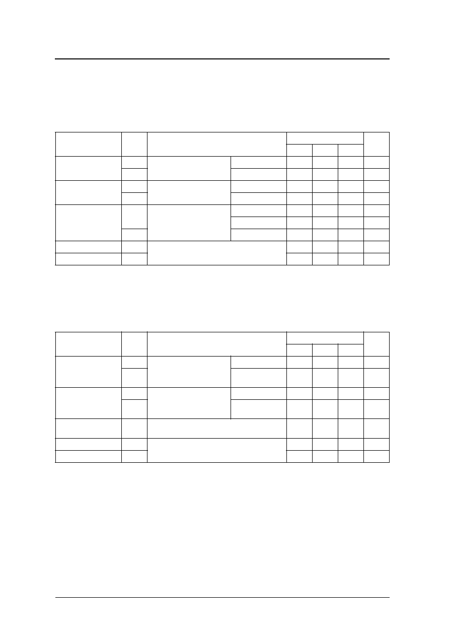
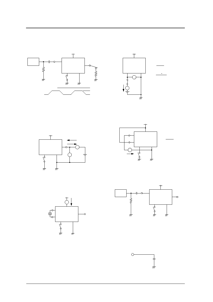
FUNCTIONAL DESCRIPTION
Standby Function
When INHN goes LOW, the oscillator stops and the oscillator output on Q becomes high impedance.
Power-saving Pull-up Resistor
The INHN pull-up resistance changes in response to the input level (HIGH or LOW). When INHN goes LOW
(standby state), the pull-up resistance becomes large to reduce the current consumption during standby.
INHN
Q
Oscillator
HIGH (or open)
f
O
output frequency
Normal operation
LOW
High impedance
Stopped
CF5020 series
NIPPON PRECISION CIRCUITS INC.--10
MEASUREMENT CIRCUITS
Measurement cct 1
2Vp-p, 10MHz sine wave input signal
C1: 0.001
�F
R1: 50
R2: 219
(2.5V operation)
275
(3.0V operation)
Measurement cct 2
Measurement cct 3
Signal
Generator
VDD
VSS
XT
Q
R1
R2
V
OH
0V
Q output
V
DD
C1
XTN
INHN
V
OH
V
OL
V
A
I
Z
VDD
VSS
XT
Q
XTN
INHN
I
Z
, I
OL
X'tal
I
DD
I
ST
A
VDD
VSS
XT
Q
XTN
INHN
Measurement cct 4
Measurement cct 5
Measurement cct 6
2Vp-p, 10MHz sine wave input signal
C1: 0.001
�F
R1: 50
Load cct 1
I
PR
A
V
V
PR
V
DD
I
PR
(V
PR
= V
SS
)
R
UP2
=
I
PR
(V
PR
=
0.7V
DD
)
V
DD
V
PR
R
UP1
=
VDD
VSS
XT
Q
XTN
INHN
I
Rf
R
f
=
V
DD
I
Rf
A
VDD
VSS
XT
Q
XTN
INHN
Signal
Generator
VDD
VSS
XT
Q
R1
C1
XTN
INHN
Q output
C
L
(Including probe
capacitance)
CF5020 series
NIPPON PRECISION CIRCUITS INC.--11
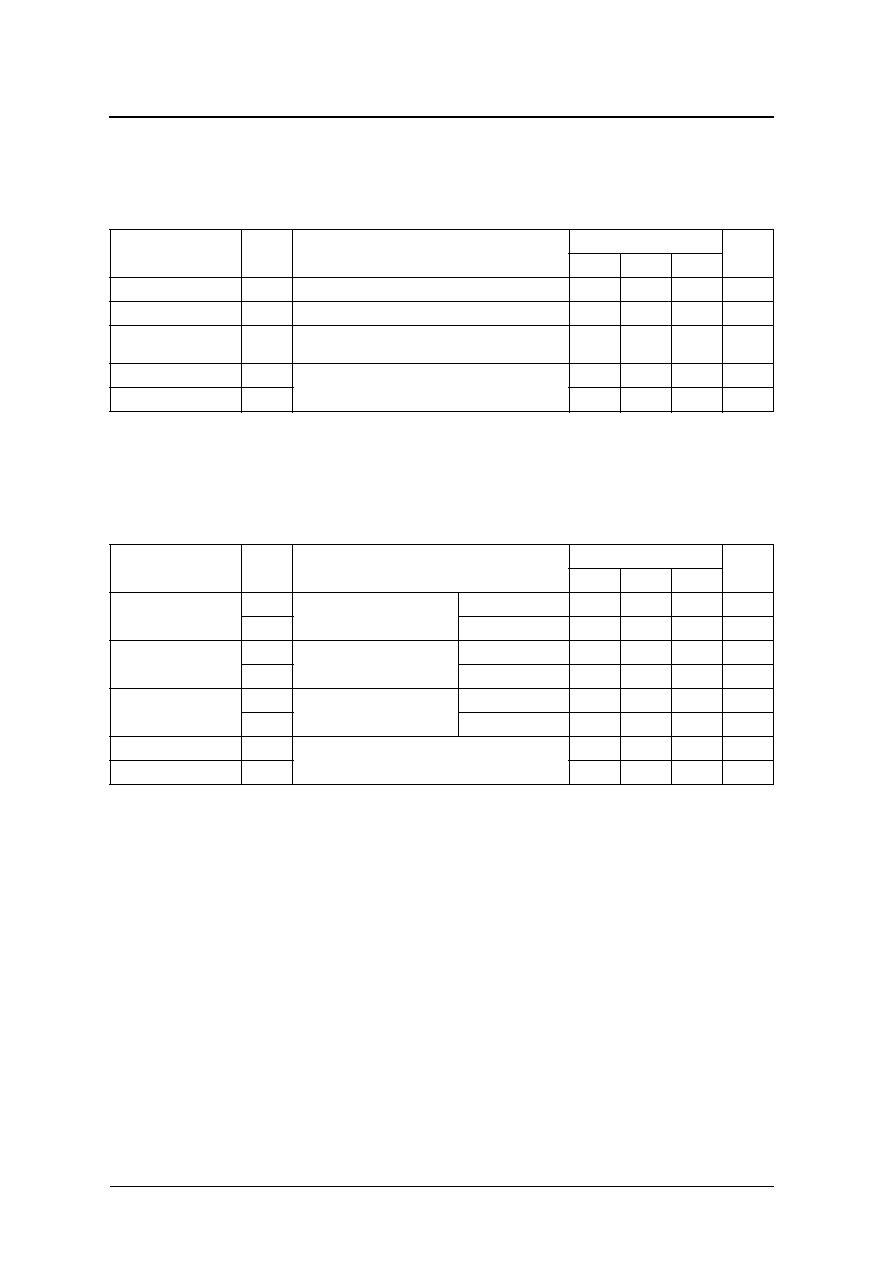
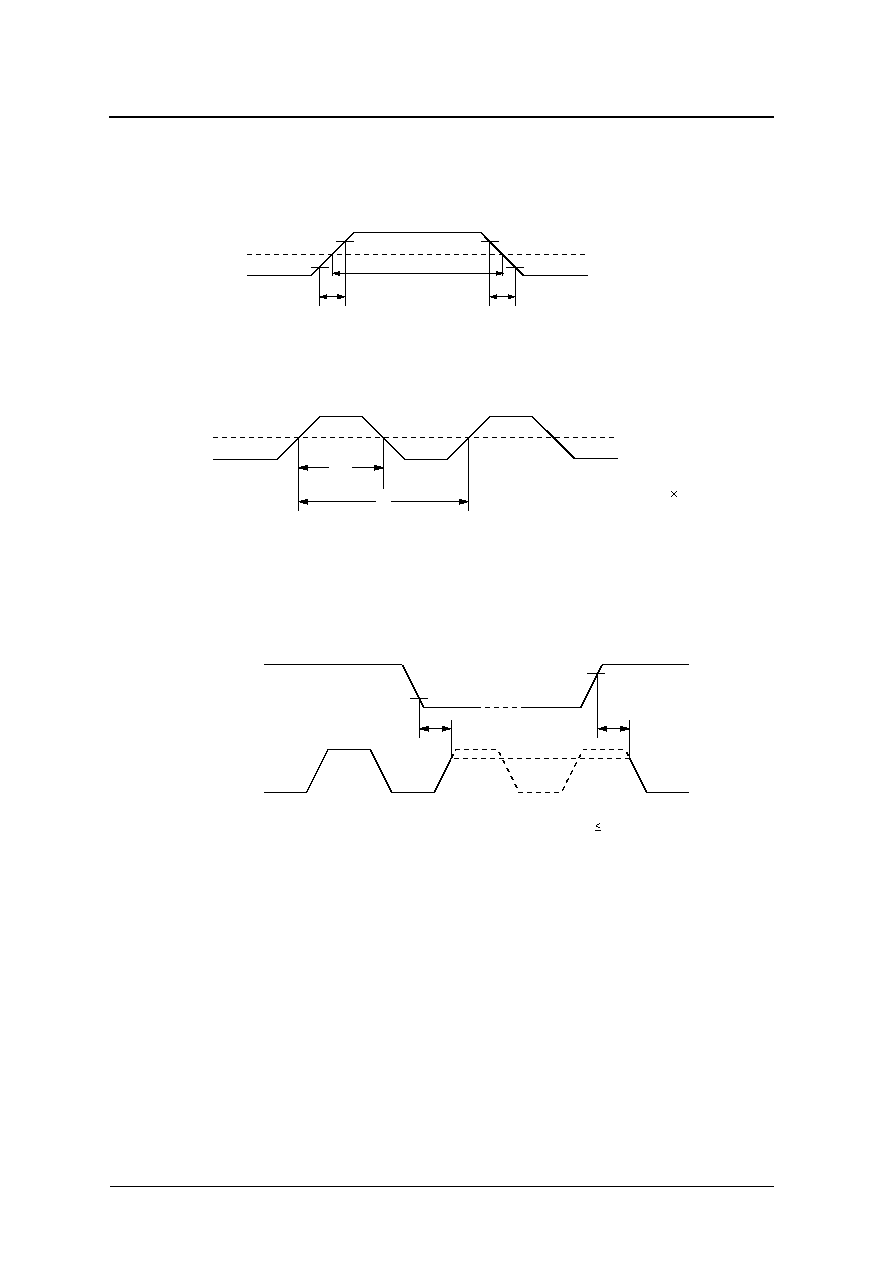
Switching Time Measurement Waveform
Output duty level, t
r
, t
f
Output duty cycle
Output Enable/Disable Delay
when the device is in standby, the oscillator stops. When standby is released, the oscillator starts and stable
oscillator output occurs after a short delay.
0.9V
DD
0.1V
DD
0.9V
DD
0.1V
DD
t
r
t
f
Q output
DUTY measurement
voltage (0.5V
DD
)
T
W
DUTY measurement
voltage
(
0.5V
DD
)
Q output
T
W
T
DUTY= T
W
/ T 100 (%)
Q output
INHN
V
IH
V
IL
t
PLZ
t
PZL
INHN input waveform
t
r =
t
f 10ns

CF5020 series
NIPPON PRECISION CIRCUITS INC.--12
NC0305CE
2004.11
Please pay your attention to the following points at time of using the products shown in this document.
The products shown in this document (hereinafter "Products") are not intended to be used for the apparatus that exerts harmful influence on
human lives due to the defects, failure or malfunction of the Products. Customers are requested to obtain prior written agreement for such
use from NIPPON PRECISION CIRCUITS INC. (hereinafter "NPC"). Customers shall be solely responsible for, and indemnify and hold NPC
free and harmless from, any and all claims, damages, losses, expenses or lawsuits, due to such use without such agreement. NPC reserves
the right to change the specifications of the Products in order to improve the characteristic or reliability thereof. NPC makes no claim or
warranty that the contents described in this document dose not infringe any intellectual property right or other similar right owned by third
parties. Therefore, NPC shall not be responsible for such problems, even if the use is in accordance with the descriptions provided in this
document. Any descriptions including applications, circuits, and the parameters of the Products in this document are for reference to use the
Products, and shall not be guaranteed free from defect, inapplicability to the design for the mass-production products without further testing
or modification. Customers are requested not to export or re-export, directly or indirectly, the Products to any country or any entity not in
compliance with or in violation of the national export administration laws, treaties, orders and regulations. Customers are requested
appropriately take steps to obtain required permissions or approvals from appropriate government agencies.
NIPPON PRECISION CIRCUITS INC.
4-3, Fukuzumi 2-chome, Koto-ku,
Tokyo 135-8430, Japan
Telephone: +81-3-3642-6661
Facsimile: +81-3-3642-6698
http://www.npc.co.jp/
Email: sales
@
npc.co.jp