preliminary
SM5022 series
NIPPON PRECISION CIRCUITS--1
NIPPON PRECISION CIRCUITS INC.
Crystal Oscillator Module ICs
OVERVIEW
The SM5022 series are crystal oscillator module ICs
fabricated in NPC's Molybdenum-gate CMOS, that
incorporate high-frequency, low current consump-
tion oscillator and output buffer circuits. Highly
accurate thin-film feedback resistors and high-fre-
quency capacitors are built-in, eliminating the need
for external components to make a stable fundamen-
tal-harmonic oscillator.
FEATURES
s
Up to 30MHz operation
s
Fundamental oscillation
s
Capacitors CG, CD built-in
s
Inverter amplifier feedback resistor built-in
s
TTL input level
s
4 mA (V
DD
= 2.7 V) drive capability
8 mA (V
DD
= 4.5 V) drive capability
s
Output three-state function
s
2.7 to 5.5 V supply voltage (A
◊
series)
4.5 to 5.5 V supply voltage (B
◊
series)
s
Oscillator frequency output (f
O
, f
O
/2, f
O
/4, f
O
/8
determined by internal connection)
s
6-pin SOT (SM5022
◊◊
H)
s
Chip form (CF5022
◊◊
)
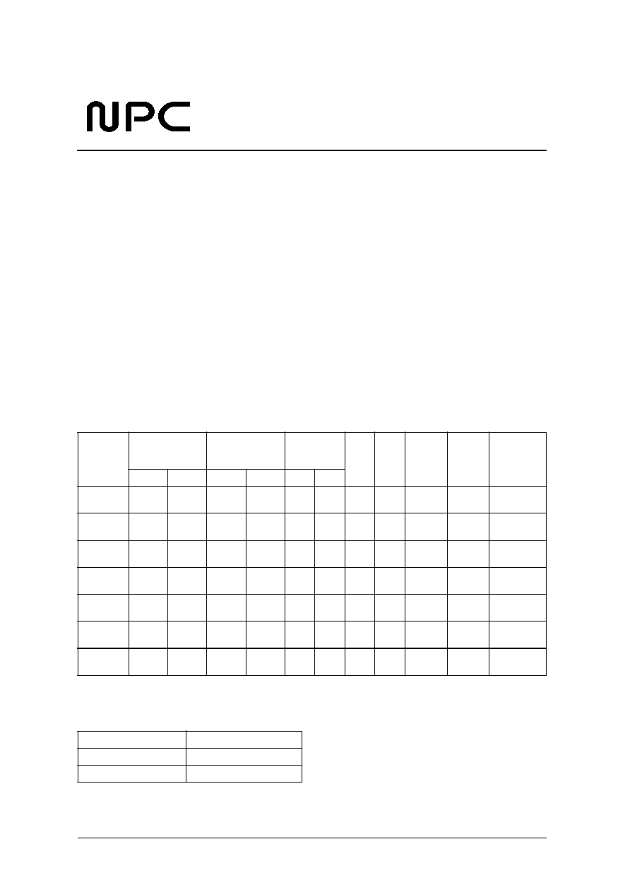
SERIES CONFIGURATION
ORDERING INFORMATION
V ersion
1
1. Chip form d evices have designation CF5022
◊◊
.
S u p p ly voltag e
R e c o m m e n d e d
operating frequency
r a n g e (MHz)
Built-in
capacitance
(pF)
g m
ratio
Rf
(k
)
Output
frequency
Output
level
S t a n d by
output state
C h i p
S O T
3 V
5 V
C
G
C
D
S M 5 0 2 2 A 1 H
2.7 to 5.5
2.7 to 5.5
4 to 24
4 to 30
8
1 0
1
6 0 0
fo
C M O S
High
i m p e d a n c e
S M 5 0 2 2 A 2 H
2.7 to 5.5
2.7 to 5.5
4 to 24
4 to 30
≠
≠
1
6 0 0
fo
C M O S
High
i m p e d a n c e
S M 5 0 2 2 A 3 H
2.7 to 5.5
2.7 to 5.5
4 to 30
4 to 30
8
1 0
1
6 0 0
fo/2
C M O S
High
i m p e d a n c e
S M 5 0 2 2 A 4 H
2.7 to 5.5
2.7 to 5.5
4 to 30
4 to 30
≠
≠
1
6 0 0
fo/2
C M O S
High
i m p e d a n c e
S M 5 0 2 2 A 5 H
2.7 to 5.5
2.7 to 5.5
4 to 30
4 to 30
8
1 0
1
6 0 0
fo/4
C M O S
High
i m p e d a n c e
S M 5 0 2 2 A 7 H
2.7 to 5.5
2.7 to 5.5
4 to 30
4 to 30
8
1 0
1
6 0 0
fo/8
C M O S
High
i m p e d a n c e
S M 5 0 2 2 B 1 H
4.5 to 5.5
4.5 to 5.5
◊
4 to 30
8
1 0
1
6 0 0
fo
T T L
High
i m p e d a n c e
D e vice
P a ck ag e
S M 5 0 2 2
◊◊
H
6-pin SOT
C F 5 0 2 2
◊◊
≠ 2
Chip form

preliminary
SM5022 series
NIPPON PRECISION CIRCUITS--3
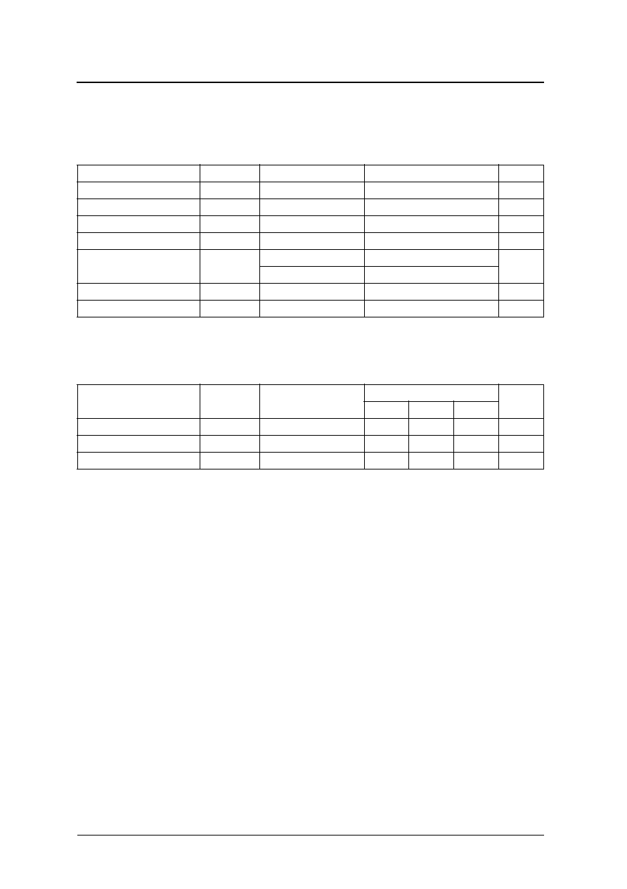
PAD LAYOUT
(Unit :
µ
m)
PINOUT
(Top View)
PIN DESCRIPTION and PAD DIMENSIONS
BLOCK DIAGRAM
Chip size: 1.00
◊
0.80 mm
Chip thickness: 220 ± 30 µm
Chip base: V
D D
level
Q
VDD
XT
VSS
(0,0)
(1000,800)
INH
XT
HA5022
1
XT
VSS
Q
VDD
2
3
6
5
4
2
XT
INH
N u m b e r
N a m e
I/O
Description
P ad dimensions [µm]
X
Y
1
I N H
I
Output state control input. High impedance when LOW . Pull-up resistor built in
8 3 4
2 1 7
2
X T
I
Amplifier input.
Cr ystal oscillator connection pins.
Cr ystal oscillator connected between XT and X T
6 3 7
2 1 7
3
V S S
≠
G r o u n d
1 6 5
1 6 5
4
Q
O
Output. Output frequency (f
O
, f
O
/2, f
O
/4, f
O
/8) determined by internal connection
1 6 2
6 3 7
5
V D D
≠
Supply voltage
8 5 9
4 5 0
6
X T
O
Amplifier output.
Cr ystal oscillator connection pins.
Cr ystal oscillator connected between XT and X T
8 0 4
6 0 4
XT
VSS
VDD
Q
C
G
C
D
R
f
XT
INH
1/2
1/2
1/2
(INH : Low active)
preliminary
SM5022 series
NIPPON PRECISION CIRCUITS--4
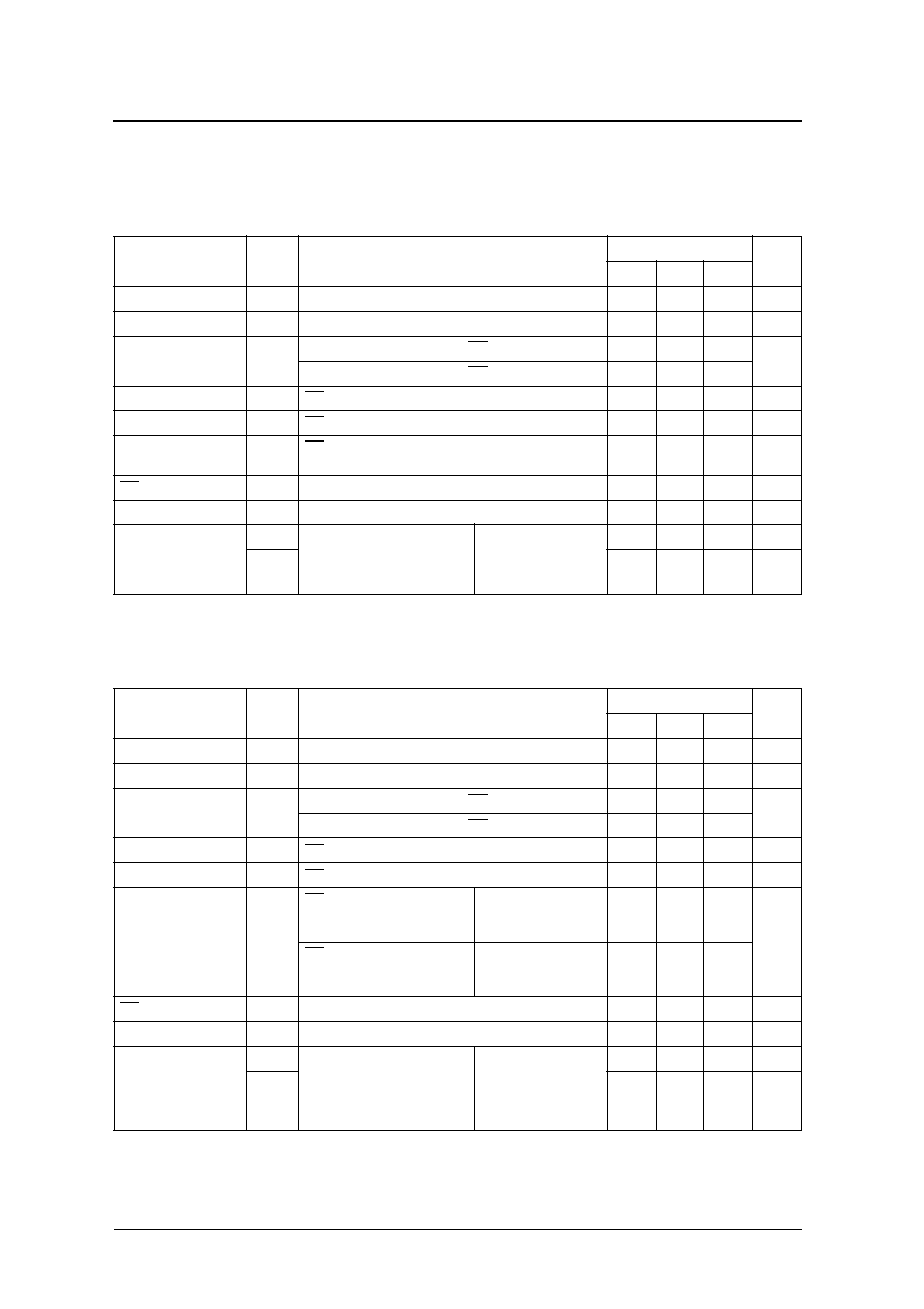
SPECIFICATIONS
Absolute Maximum Ratings
V
SS
= 0 V
Recommended Operating Conditions
V
SS
= 0 V, f
30MHz, C
L
15pF
Note: R e c o m m e n d e d o p e rating conditions will change in accordance with operating frequency, load capacitance, or pow er dissipation.
P arameter
S y m b o l
Condition
Rating
Unit
Supply voltage ra n g e
V
D D
-
0.5 to 7.0
V
Input voltage ra n g e
V
IN
-
0.5 to V
D D
+ 0.5
V
Output voltage ra n g e
V
O U T
-
0.5 to V
D D
+ 0.5
V
O p e rating temperature ra n g e
T
opr
-
40 to 85
∞
C
Storage temperature ra n g e
T
stg
Chip form
-
65 to 150
∞
C
6-pin SOT
-
55 to 125
Output current
I
O U T
1 3
m A
P ow er dissipation
P
D
6-pin SOT
2 5 0
m W
P arameter
S y m b o l
Condition
Rating
Unit
m i n
typ
m a x
Supply voltage
V
D D
2.7
≠
5.5
V
Input voltage
V
IN
V
S S
≠
V
D D
V
O p e rating temperature
T
O P R
-
2 0
≠
8 0
∞
C
preliminary
SM5022 series
NIPPON PRECISION CIRCUITS--5
Electrical Characteristics
3 V operation: A
◊
series
V
DD
= 2.7 to 3.6 V, V
SS
= 0 V, Ta =
-
20 to 80
∞
C unless otherwise noted.
5 V operation: A
◊
series/ B
◊
series
V
DD
= 4.5 to 5.5 V, V
SS
= 0 V, Ta =
-
20 to 80
∞
C unless otherwise noted.
P arameter
S y m b o l
Condition
Rating
Unit
m i n
typ
m a x
HIGH-level output voltage
V
O H
Q: Measurement cct 1, V
D D
= 2.7 V, I
O H
= 4 m A
2.1
2.4
≠
V
L O W -level output voltage
V
O L
Q: Measurement cct 2, V
D D
= 2.7 V, I
O L
= 4 m A
≠
0.3
0.4
V
Output leakage current
I
Z
Q: Measurement cct 2, V
D D
= 3.6 V, I N H = L O W , V
O H
= V
D D
≠
≠
1 0
µ A
Q: Measurement cct 2, V
D D
= 3.6 V, I N H = L O W , V
O L
= V
S S
≠
≠
1 0
HIGH-level input voltage
V
IH
I N H
2.0
≠
≠
V
L O W -level input voltage
V
IL
I N H
≠
≠
0.5
V
Current consumption
I
D D
I N H = open, Measurement cct 3, load cct 1, C
L
= 15 p F,
30 MHz cr ystal oscillator
≠
4
7
m A
I N H pull-up resistance
R
U P
Measurement cct 4
2 5
1 0 0
2 5 0
k
F e e d b a ck resistance
R
f
Measurement cct 5
2 0 0
6 0 0
1 0 0 0
k
Built-in capacitance
C
G
Design value, determined by the
internal wafer pattern
S M 5 0 2 2 A 1 H , C F 5 0 2 2 A 1
S M 5 0 2 2 A 3 H , C F 5 0 2 2 A 3
S M 5 0 2 2 A 5 H , C F 5 0 2 2 A 5
S M 5 0 2 2 A 7 H , C F 5 0 2 2 A 7
7.44
8
8.56
p F
C
D
9.3
1 0
10.7
p F
P arameter
S y m b o l
Condition
Rating
Unit
m i n
typ
m a x
HIGH-level output voltage
V
O H
Q: Measurement cct 1, V
D D
= 4.5 V, I
O H
= 8 m A
3.9
4.2
≠
V
L O W -level output voltage
V
O L
Q: Measurement cct 2, V
D D
= 4.5 V, I
O L
= 8 m A
≠
0.3
0.4
V
Output leakage current
I
Z
Q: Measurement cct 2, V
D D
= 5.5 V, I N H = L O W , V
O H
= V
D D
≠
≠
1 0
µ A
Q: Measurement cct 2, V
D D
= 5.5 V, I N H = L O W , V
O L
= V
S S
≠
≠
1 0
HIGH-level input voltage
V
IH
I N H
2.0
≠
≠
V
L O W -level input voltage
V
IL
I N H
≠
≠
0.8
V
Current consumption
I
D D
I N H = open, Measurement cct 3,
load cct 1, C
L
= 15 p F,
30 MHz cr ystal oscillator
S M 5 0 2 2 A
◊
H , C F 5 0 2 2 A
◊
≠
7
1 2
m A
I N H = open, Measurement cct 3,
load cct 2, C
L
= 15 p F,
30 MHz cr ystal oscillator
S M 5 0 2 2 B
◊
H , C F 5 0 2 2 B
◊
≠
7
1 2
I N H pull-up resistance
R
U P
Measurement cct 4
2 5
1 0 0
2 5 0
k
F e e d b a ck resistance
R
f
Measurement cct 5
2 0 0
6 0 0
1 0 0 0
k
Built-in capacitance
C
G
Design value, determined by the
internal wafer pattern
S M 5 0 2 2 A 1 H , C F 5 0 2 2 A 1
S M 5 0 2 2 A 3 H , C F 5 0 2 2 A 3
S M 5 0 2 2 A 5 H , C F 5 0 2 2 A 5
S M 5 0 2 2 A 7 H , C F 5 0 2 2 A 7
S M 5 0 2 2 B 1 H , C F 5 0 2 2 B 1
7.44
8
8.56
p F
C
D
9.3
1 0
10.7
p F
