 | –≠–ª–µ–∫—Ç—Ä–æ–Ω–Ω—ã–π –∫–æ–º–ø–æ–Ω–µ–Ω—Ç: CF5034DB | –°–∫–∞—á–∞—Ç—å:  PDF PDF  ZIP ZIP |
CF5034 series
NIPPON PRECISION CIRCUITS INC.--1
350MHz PECL-output Oscillator ICs
OVERVIEW
The CF5034 series are differential LVPECL output oscillator ICs. They are made using a BiCMOS process
which allows high-frequency oscillator circuits and differential LVPECL output circuits to be fabricated on a
single chip. Two oscillator modes are supported--350MHz maximum fundamental oscillation mode, and
80MHz to 160MHz 3rd overtone oscillation mode.
The CF5034 series devices require only the connection of a crystal to realize a differential LVPECL output
oscillator circuit.
FEATURES
I
3.3 ± 0.3V operating supply voltage
I
Oscillator frequency range
∑ 80MHz to 350MHz fundamental oscillation
mode
∑ 80MHz to 160MHz 3rd overtone oscillation
mode
I
40MHz to 350MHz output frequency range
I
Differential LVPECL output
I
f
O
(oscillator frequency) or f
O
/2 output frequency,
determined by internal connection
I
50 ± 5% output duty (measured at output crossing
point)
I
Standby function: outputs are high impedance
when OE is LOW.
I
Power-saving pull-up resistor built-in (pin OE)
I
Chip form (CF5034
◊◊
)
SERIES LINEUP
ORDERING INFORMATION
Version
Oscillation mode
Recommended oscillator
frequency [MHz]
1
1. The recommended oscillator frequency criteria is based on the negative resistance characteristics and cutoff frequency. Note that this may change
depending on the crystal characteristics, thus sufficient allowance should be made.
Output frequency
CF5034AA
Fundamental
250 to 350
f
O
CF5034AB
f
O
/2
CF5034BA
160 to 250
f
O
CF5034BB
f
O
/2
CF5034DA
≠
80 to 350
(external capacitors required)
f
O
CF5034DB
f
O
/2
CF5034LA
Fundamental or
3rd overtone
125 to 160
f
O
CF5034LB
f
O
/2
CF5034MA
80 to 125
f
O
CF5034MB
f
O
/2
Device
Package
CF5034
◊◊-
1
Chip form

CF5034 series
NIPPON PRECISION CIRCUITS INC.--2
PAD LAYOUT
(Unit: µm)
PAD DESCRIPTION AND DIMENSIONS
BLOCK DIAGRAM
Chip size: 1.16
◊
1.31mm
Chip thickness: 300 ± 30µm
Chip base: GND potential
Pad No.
Name
I/O
Function
Pad dimensions [µm]
X
Y
1
VCC
≠
Supply pin
146
145
2
XIN
I
Oscillator input pin
536
145
3
XOUT
O
Oscillator output pin
809
145
4
GND
≠
Ground pin
1015
145
5
OE
I
Output enable pin. Outputs are high impedance when LOW (oscillator
stopped). Power-saving pull-up resistor built-in.
979
1165
6
TEST
I
IC test pin. Leave open circuit for normal operation.
839
1165
7
VCC2
≠
Output buffer supply pin
690
1165
8
OUTN
O
Output pin (complementary)
449
1165
9
OUT
O
Output pin (true)
216
1165
OUTN
(0,0)
(1160,1310)
X
Y
DA5034
1
2
3
4
9
8
7
6
5
OUT
VCC2
TEST
OE
VCC
XIN XOUT GND
XIN
VCC
OE
XOUT
1/2
OUT
VCC2
GND
OUTN
ECL
R
f
C
XIN
C
XOUT

CF5034 series
NIPPON PRECISION CIRCUITS INC.--3
ABSOLUTE MAXIMUM RATINGS
RECOMMENDED OPERATING CONDITIONS
ELECTRICAL CHARACTERISTICS
DC Characteristics
Recommended operating conditions unless otherwise noted.
Parameter
Symbol
Conditions
Rating
Unit
Supply voltage range
V
CC
-
0.5 to 7.0
V
Input voltage range
V
IN
GND
-
0.5 to V
CC
+ 0.5
V
Output voltage range
V
OUT
GND
-
0.5 to V
CC
+ 0.5
V
Storage temperature range
T
STG
-
65 to 150
∞
C
Parameter
Symbol
Conditions
Rating
Unit
Min
Typ
Max
Operating supply voltage
V
CC
3.0
3.3
3.6
V
Input voltage
V
IN
GND
≠
V
CC
V
Operating temperature
T
OPR
-
40
25
85
∞
C
Output load
RL
Terminated to V
CC
-
2V
≠
50
≠
Output frequency
f
OUT
40
≠
350
MHz
Parameter
Symbol
Conditions
Rating
Unit
Min
Typ
Max
Current consumption 1
I
EE1
Measurement cct. 1, OE = open
≠
55
88
mA
Current consumption 2
I
EE2
Measurement cct. 1, OE = LOW
≠
≠
30
µA
OUT/OUTN HIGH-level output voltage
V
OH
Measurement cct. 4,
V
CC
= 3.3V,
OE = open
Ta = 0 to 85
∞
C
2.275
2.350
2.420
V
Ta = ≠ 40
∞
C
2.215
2.295
2.420
V
OUT/OUTN LOW-level output voltage
V
OL
Ta = 0 to 85
∞
C
1.490
1.600
1.680
V
Ta = ≠ 40
∞
C
1.470
1.605
1.745
V
OUT/OUTN output leakage current
I
Z
Measurement cct. 2, OE = LOW
≠
≠
10
µA
OE HIGH-level input voltage
V
IH
Measurement cct. 1
0.7V
CC
≠
≠
V
OE LOW-level input voltage
V
IL
Measurement cct. 1
≠
≠
0.3V
CC
V
OE LOW-level input current 1
I
IL1
Measurement cct. 2, V
IL
= 0V
-
2
≠
-
20
µA
OE LOW-level input current 2
I
IL2
Measurement cct. 2, V
IL
= 0.7V
CC
-
20
≠
-
200
µA

CF5034 series
NIPPON PRECISION CIRCUITS INC.--4
AC Characteristics
Recommended operating conditions unless otherwise noted.
Parameter
Symbol
Conditions
Rating
Unit
Min
Typ
Max
Output duty cycle 1
Duty 1
Measurement cct. 3,
measured at output crossing point,
Ta = 25
∞
C, V
CC
= 3.3V
45
≠
55
%
Output duty cycle 2
Duty 2
Measurement cct. 3,
measured at 50% output swing,
Ta = 25
∞
C, V
CC
= 3.3V
45
≠
55
%
Output swing
1
1. The said values are measured by using the NPC standard jig.
V
Opp
Measurement cct. 1, Ta = T
OPR
, f = 350MHz,
Peak to peak of output waveform
0.4
≠
≠
V
Output rise time
t
r
Measurement cct. 3,
20 to 80% output swing
≠
0.5
1
ns
Output fall time
t
f
Measurement cct. 3,
80 to 20% output swing
≠
0.5
1
ns
Output enable time
2
2. The built-in oscillator stop function does not operate with normal output immediately when OE goes HIGH. Instead, normal output occurs after the
oscillator startup time has elapsed.
t
OE
Measurement cct. 1, Ta = 25
∞
C
≠
≠
200
ns
Output disable time
2
t
OD
Measurement cct. 1, Ta = 25
∞
C
≠
≠
200
ns
Timing chart
t
r
t
f
OUTN
OUT
80%
20%
V
DD
≠ 2V
V
OH
V
OL
V
DD
t
W
t
PER
OE
V
SS
V
DD
V
SS
t
OE
t
OD
V
IH
V
IL
DUTY =
t
W
/
t
PER
100
OE input waveform
t
r
=
t
f
10ns
V
Opp
CF5034 series
NIPPON PRECISION CIRCUITS INC.--5
FUNCTIONAL DESCRIPTION
Standby Function
When OE goes LOW, the oscillator stops and the
output pins (OUT, OUTN) become high impedance.
Power-saving Pull-up Resistor
The OE pin pull-up resistance changes in value in
response to the input level (HIGH or LOW). When
OE is LOW (standby state), the pull-up resistance
increases, thereby decreasing the current consump-
tion.
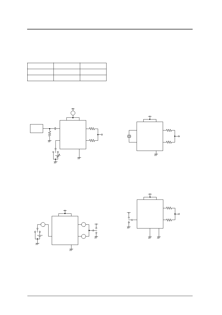
MEASUREMENT CIRCUITS
Measurement Circuit 1
Measurement Circuit 2
Measurement Circuit 3
Measurement Circuit 4
OE
OUT, OUTN
Oscillator
HIGH (or open)
Either f
O
or f
O
/2
Normal operation
LOW
High impedance
Stopped
XIN input signal 500mVp-p, sine wave
C1: 0.001µF
R1: 50
V
T
: V
CC
-
2V
V
OE
: V
CC
, V
IH
, V
IL
Signal
Generator
VCC
R1
C1
XIN
OE
VCC2
OUT
GND
OUTN
V
OE
R1
R1
V
T
A
I
EE1,
I
EE2
0.7V
CC
A
A
A
VCC
OE
VCC2
OUT
GND
OUTN
R1: 50
, V
T
: V
CC
-
2V
R1: 50
, V
T
: V
CC
-
2V
XOUT = HIGH: OUT pin is fixed HIGH (V
OH
).
OUTN pin is fixed LOW (V
OL
).
XOUT = LOW: OUT pin is fixed LOW (V
OL
).
OUTN pin is fixed HIGH (V
OH
).
VCC
XIN
XOUT
VCC2
OUT
GND
OUTN
R1
R1
V
T
VCC
XIN
XOUT
VCC2
OUT
GND
OUTN
R1
R1
V
T
TEST