CF5073 series
NIPPON PRECISION CIRCUITS INC.--1
VCXO Module ICs with Built-in Varicap
OVERVIEW
The CF5073 series are VCXO ICs with built-in varicap diode. They use a recently developed negative-resis-
tance switching oscillation circuit, at oscillation startup and during normal oscillation, for both good oscilla-
tion startup characteristics and wide pullrange. Furthermore, it employs a CMOS process varicap diode, and
also features all the necessary VCXO structure circuit components on a single chip, forming a VCXO module
with just the connection of an external crystal.
FEATURES
I
3.0 to 3.6V supply voltage range
I
10MHz to 60MHz operating frequency
(varies with version)
I
Uses negative-resistance switching function
I
Varicap diode built-in
I
Frequency divider built-in (varies with version: f
O
,
f
O
/2, f
O
/4, f
O
/8, f
O
/16, f
O
/32)
I
CMOS output level
I
50 � 10% output duty
I
6mA (min) output drive capability
I
15pF output load capacitance C
L
I
Standby function
(high impedance in standby mode)
I
Chip form (CF5073
��
)
SERIES LINEUP
APPLICATIONS
I
VCXO modules
I
Communications application
I
Networking application
I
Broadcasting application
ORDERING INFORMATION
Version
Typical oscillation
frequency
1
[MHz]
1. The typical oscillation frequency is the oscillation frequency criteria for use when selecting the device version. Note that the oscillation
characteristics and pullability vary with the crystal used and the mounting conditions. Even for the same frequency, the optimal version can vary
with crystal characteristics, so careful evaluation should be exercised when selecting the device version.
Output frequency
CF5073
�
1
CF5073
�
2
2
2. These versions are produced after receiving a purchase order. Please ask our Sales & Marketing section for further detail.
CF5073
�
3
2
CF5073
�
4
2
CF5073
�
5
2
CF5073
�
6
2
CF5073A
�
16
f
O
f
O
/2
f
O
/4
f
O
/8
f
O
/16
f
O
/32
CF5073B
�
23
CF5073C
�
30
CF5073D
�
37
CF5073E
�
44
CF5073F
�
51
Device
Package
CF5073
��-
1
Chip form

CF5073 series
NIPPON PRECISION CIRCUITS INC.--2
PAD LAYOUT
(Unit: �m)
PAD DESCRIPTION AND DIMENSIONS
Chip size: 1.24
�
1.4mm
Chip thickness: 300 � 30�m
Chip base: V
DD
potential
Pad No.
Name
I/O
Description
Function
Pad dimensions [�m]
X
Y
1
VC
I
Oscillation frequency control
voltage input pin
Positive polarity (frequency increases with
increasing voltage)
134
915
2
INHN
I
Output state control voltage
input pin
High-impedance output when LOW, pull-up
resistor built-in
137
295
3
VSS
�
(
-
) supply pin
458
137
4
Q
O
Output pin
Output frequency determined by internal
circuit to one of f
O
, f
O
/2, f
O
/4, f
O
/8, f
O
/16, f
O
/32
1086
155
5
VDD
�
(+) supply pin
1106
772
6
XT
I
Amplifier input pin
Crystal connection pins.
Crystal is connected between XT and XTN.
829
1263
7
XTN
O
Amplifier output pin
416
1260
XT
VC
(0,0)
(1240,1400)
HA5073
XTN
INHN
VSS
Q
VDD
1
2
3
4
5
6
7
CF5073 series
NIPPON PRECISION CIRCUITS INC.--3
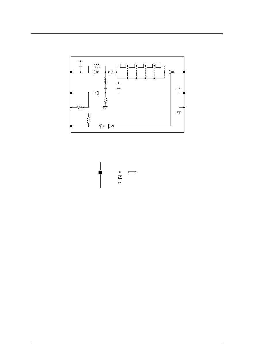
BLOCK DIAGRAM
Note. ESD of XT pin is inferior to other pins.
ESD of all pins excluding XT pin is equivalent to that of our other oscillator products.
VC pin has no protection circuit at V
DD
side. (See figure below.)
XTN
Q
C
G
R
f
XT
INHN
VC
C
D
C
C
C
V
R
D
R
B
1
R
B
2
R
UP
VDD
VSS
1/2
1/2
1/2
1/2
1/2
VC
Internal circuit
CF5073 series
NIPPON PRECISION CIRCUITS INC.--4
ABSOLUTE MAXIMUM RATINGS
V
SS
= 0V unless otherwise noted.
RECOMMENDED OPERATING CONDITIONS
V
SS
= 0V, f = 10MHz to 60MHz, C
L
15pF unless otherwise noted.
Parameter
Symbol
Conditions
Rating
Unit
Supply voltage range
V
DD
-
0.5 to 7.0
V
Input voltage range
V
IN
All input pins excluding VC pin
-
0.5 to V
DD
+ 0.5
V
VC pin
-
0.5 to V
DD
+ 2.5
1
1. It should not exceed + 7.0V.
V
Output voltage range
V
OUT
-
0.5 to V
DD
+ 0.5
V
Operating temperature range
T
opr
-
40 to +85
�
C
Storage temperature range
T
STG
-
65 to +150
�
C
Output current
I
OUT
20
mA
Parameter
Symbol
Conditions
Rating
Unit
Min
Typ
Max
Operating supply voltage
V
DD
3.0
�
3.6
V
Input voltage
V
IN
V
SS
�
V
DD
V
Operating temperature
T
OPR
�40
�
+85
�
C

CF5073 series
NIPPON PRECISION CIRCUITS INC.--5
ELECTRICAL CHARACTERISTICS
CF5073A
�
V
DD
= 3.0 to 3.6V, V
C
= 1.65V, V
SS
= 0V, Ta = �40 to +85
�
C, unless otherwise noted.
Parameter
Symbol
Conditions
Rating
Unit
Min
Typ
Max
HIGH-level output voltage
V
OH
Q: Measurement circuit 1, I
OH
= 6mA
2.5
2.75
�
V
LOW-level output voltage
V
OL
Q: Measurement circuit 1, I
OL
= 6mA
�
0.2
0.4
V
Output leakage current
I
Z
Q: Measurement circuit 6,
INHN = LOW
V
OH
= V
DD
�
�
10
�A
V
OL
= V
SS
�
�
10
�A
HIGH-level input voltage
V
IH
INHN
0.7V
DD
�
�
V
LOW-level input voltage
V
IL
INHN
�
�
0.3V
DD
V
Current consumption
I
DD
Measurement circuit 2,
load circuit 1,
INHN = open, C
L
= 15pF,
f = 16MHz
CF5073A1
�
8
20
mA
CF5073A2
�
7.5
19.5
mA
CF5073A3
�
7
19.5
mA
CF5073A4 to 6
�
7
19
mA
INHN pull-up resistance
R
UP
Measurement circuit 3
50
100
180
k
Built-in resistance
R
f
Design value, determined by internal wafer
pattern
150
300
540
k
R
D
0.67
0.96
1.25
k
R
B1
Measurement circuit 4
100
200
360
k
R
B2
Design value, determined by internal wafer
pattern
50
100
180
k
Built-in capacitance
C
V
Design value, determined
by internal wafer pattern
V
C
= 0.3V
11.0
14.4
17.8
pF
V
C
= 3.0V
2.4
4.0
5.6
pF
C
G
Design value, determined by internal wafer
pattern
25.5
30
34.5
pF
C
D
34
40
46
pF
C
C
8.5
10
11.5
pF