 | –≠–ª–µ–∫—Ç—Ä–æ–Ω–Ω—ã–π –∫–æ–º–ø–æ–Ω–µ–Ω—Ç: CF5741BA | –°–∫–∞—á–∞—Ç—å:  PDF PDF  ZIP ZIP |

CF5741 series
NIPPON PRECISION CIRCUITS--1
NIPPON PRECISION CIRCUITS INC.
Analog Clock CMOS IC
OVERVIEW
The CF5741 series are analog clock driver ICs
using 32.768kHz reference frequency of crystal
oscillator. Some versions in accordance with the
combinations of each motor drive and alarm output
characteristics can provide a wide range of applica-
tions for various clock specifications.
FEATURES
s
Operating voltage 1.2 to 2.0V
s
Low current 1.2
µ
A (typ) / 1.5V
s
Built-in oscillator circuits (32.768 kHz)
s
Built-in crystal oscillator capacitors (C
G
, C
D
)
s
Motor output
Various motor output
s
Alarm output
Various alarm output
s
Reset function
s
Input debounce function (AI, RST/TC)
s
Chip form (CF5741
◊◊
)
PINOUT
(Top View)
SERIES LINEUP
ORDERING INFORMATION
Chip size : 1.22
◊
1.20 mm
Chip thickness : 400
±
30
µ
m
Pad size : 100
◊
100
µ
m
Reverse side : V
DD
level
1
XT
VSS
(0,0)
X
Y
SA5741
2
3
4
5
10
9
8
7
6
XTN
AO2/F
AO1
VDD
OUT2
AI
RST/TC
OUT1
CF5741AA
CF5741AB
CF5741BA
CF5741BB
Built-in capacitor
XT terminal C
G
(pF)
0
25
0
27
XTN terminal C
D
(pF)
25
25
25
25
Reset input
Active level
Low
(Pull-up resistor)
Low
(Pull-up resistor)
Low
(Pull-up resistor)
Low
(Pull-up resistor)
Motor output
Active level
High
High
High
High
Hand drive cycle t
CY
(sec)
1
1
1
1
Pulse width t
PW
(msec)
31.25
31.25
46.875
46.875
Alarm input
Active level
Low
(Pull-up resistor)
Low
(Pull-up resistor)
Low
(Pull-up resistor)
Low
(Pull-up resistor)
Test function (1/2V
DD
)
Yes
Yes
Yes
Yes
Alarm output
Terminal
AO1
AO2/F
AO1
AO2/F
AO1
AO2/F
1
1. AO is complete reverse phase of AO. (even output is inactive.)
AO1
AO2/F
1
Active level
High
High
High
High
High
Low
High
Low
Fundamental frequency f
PW
(Hz)
2048
32
2048
32
2048
2048
2048
2048
Modulation frequency f
CY
(Hz)
8
+
1
-
8
+
1
-
8
+
1
8
+
1
8
+
1
8
+
1
Device
Package
CF5741
◊◊
Chip form
CF5741 series
NIPPON PRECISION CIRCUITS--2
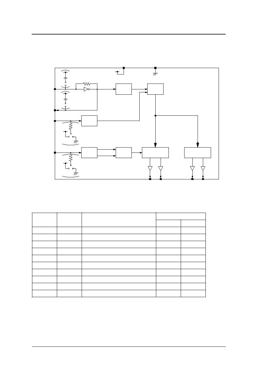
BLOCK DIAGRAM
PIN DESCRIPTION
Number
Name
Description
Dimensions (
µ
m)
X
Y
1
VSS
Ground
147
1048
2
AO1
Alarm signal output1
147
867
3
AO2 / F
Alarm signal output2/Frequency output
147
685
4
XTN
Crystal oscillator connection
146
446
5
XT
Crystal oscillator connection
146
206
6
VDD
Power supply pin
1072
147
7
RST / TC
Reset/Test clock input
1073
386
8
AI
Alarm input
1073
626
9
OUT1
Motor drive output 1
1072
867
10
OUT2
Motor drive output 2
1072
1048
4 Stage
Divider
13 Stage
Divider
Reset
Input
Alarm
Input
AO
Test
Alarm Output
Control
Motor Output
Control
VDD
VSS
AO1 AO2/F
OUT1 OUT2
XT
RST/TC
AI
Alarm
Test
XTN
C
D
C
G
CF5741 series
NIPPON PRECISION CIRCUITS--3
SPECIFICATIONS
Absolute Maximum Ratings
Electrical Characteristics
Ta
=
25
∞
C, V
DD
=
1.5V, V
SS
=
0V, X
tal (fo
=
32.768kHz, C
I
35k
), unless otherwise noted.
Parameter
Symbol
Condition
Rating
Unit
Supply voltage
V
DD
-
V
SS
-
0.3 to 5.0
V
Input voltage
V
IN
V
SS
V
IN
V
DD
V
Operating temperature
T
OPR
-
30 to 80
∞
C
Storage temperature
T
STG
-
65 to 150
∞
C
Parameter
Symbol
Condition
Rating
Unit
min
typ
max
Supply voltage
V
DD
1.2
1.5
2.0
V
Current consumption
I
DD
OUT1, OUT2
=
Open
1.2
4.0
µ
A
Oscillator start-up time
t
STA
V
DD
=
1.2V
5.0
sec
V
DD
=
1.5V
2.0
sec
Motor output current
I
MOT
V
DD
=
1.2V, R
L
=
200
1
1. R
L
is resistor of motor coil, that connect OUT1 between OUT2.
4.0
mA
Input resistance
2
(AI, RST/TC)
2. R
IN
=
V
DD
/I
IS
. I
IS
is current that flow into VSS from AI, RST/TC, when AI, RST/TC short VSS. (AI,RST/TC build-in pull-up resistor.)
R
IN
200
1200
k
Oscillator stability
f/f
V
DD
=
1.2V to 2.0V
0.5
1.0
ppm / 0.1V
Alarm output current
(AO1, AO2/F)
I
OL1
V
OL
=
0.75V
900
µ
A
I
OL2
V
OL
=
0.75V
10
µ
A
I
OH1
V
OH
=
0.75V
900
µ
A
I
OH2
V
OH
=
0.75V
10
µ
A
Frequency output voltage
V
F
V
DD
=
1.2V, C
L
=
50pF
0.4
V
Internal capacitance
3
3. C
G
is internal capacitor between VDD and XT. C
D
is internal capacitor between VDD and XTN.
C
G
pF
C
D
pF
CF5741 series
NIPPON PRECISION CIRCUITS--4
FUNCTIONAL DESCRIPTION
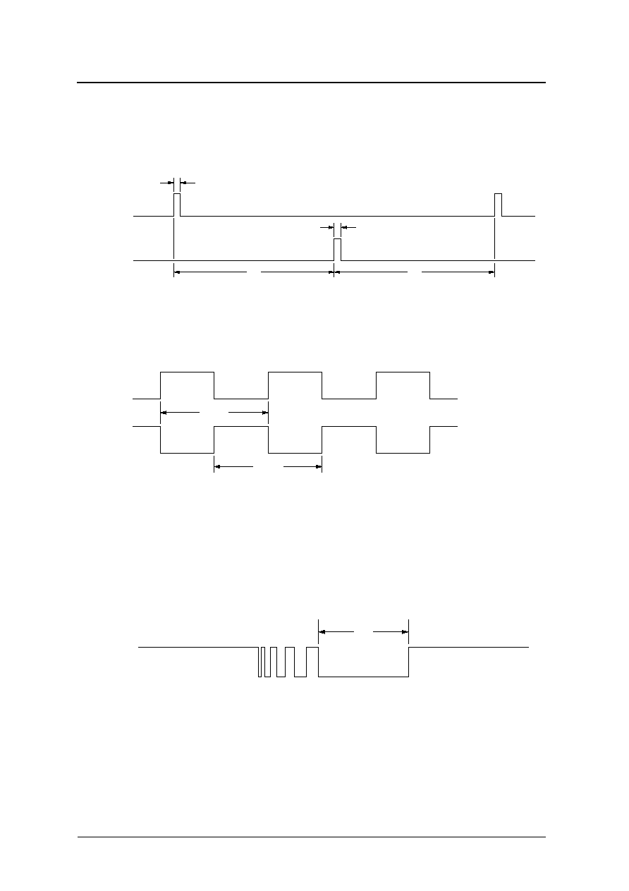
Motor Output
Stepping motor drive type
Sweeping motor drive type
Input Debounce Function (AI ,RST/TC)
Setting bouncing delay time prevents the circuit from the erroneous operation by AI and RST/TC input
bouncing.
t
ON
<
62.5 msec : Alarm and reset input is ignored.
62.5
t
ON
125 msec : Alarm and reset input is ignored or accepted.
t
ON
>
125 msec : Alarm and reset input is accepted.
OUT1
(Active High)
OUT2
(Active High)
t
PW
t
PW
t
CY
1sec
t
CY
1sec
t
CY
: Needle period
t
PW
: Pulse width
OUT1
OUT2
t
CY
125msec
t
CY
125msec
t
CY
: Needle period
t
PW
: Pulse width
t
ON
AI , RST/TC
(Active Low)

CF5741 series
NIPPON PRECISION CIRCUITS--5
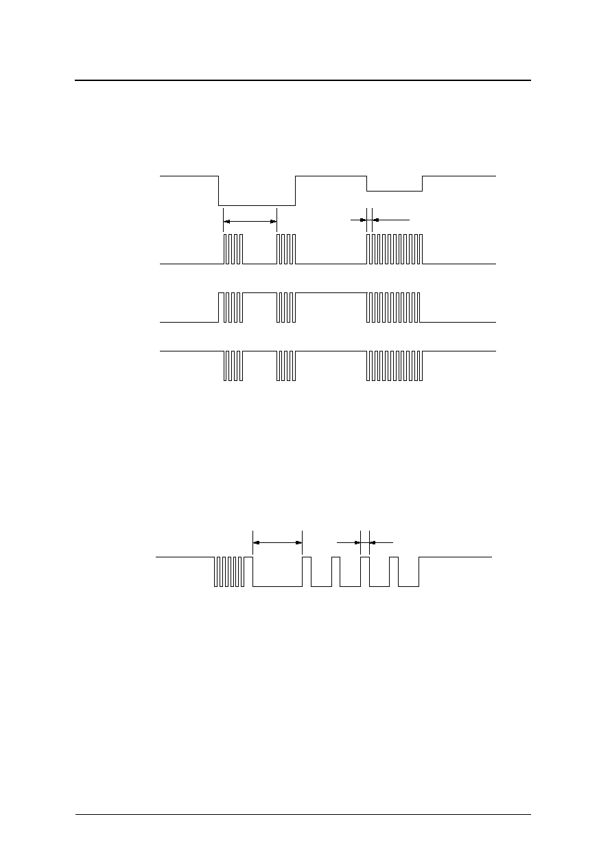
Reset Function
RST/TC goes to active level when motor output can be stopped. Motor output(AO1,AO2) restart of another
stopped output after reset off.
Alarm Output
Alarm input/output
*1 : AO2 / F is the reverse phase of AO1, when output is active.
*2 : AO2 / F is complete reverse phase of AO1.
f
PW
: Alarm fundamental frequency
f
CY
: Alarm modulation frequency
OUT1
(Active High)
OUT2
(Active High)
t
PW
t
PW
t
CY
t
CY
RST/TC
(Active Low)
t
CY
+
0
-
125msec
t
ON
AO1
(Active High)
AO2/F
(Active High)
AI
(Active Low)
AO2/F
(Active Low)
f
PW
(Hz)
f
CY
(Hz)
t
ON
*2
*1
CF5741 series
NIPPON PRECISION CIRCUITS--6
Test Function
Fundamental frequency alarm output function
AI goes to 1/2V
DD
when AO1 and AO2 output alarm fundamental frequency. This frequency can used to
adjust frequency.
Gain fast function
RST/TC is active level more than 125 msec. And RST/TC input outside clock when motor output gain fast.
t
CPW
is more less than 0.9765625 msec.
*1 : AO2 / F is the reverse phase of AO1, when output is active.
*2 : AO2 / F is complete reverse phase of AO1.
f
PW
: Alarm fundamental frequency
f
CY
: Alarm modulation frequency
t
RES
125msec
t
CPW
0.9765625msec
AO1
(Active High)
AO2/F
(Active High)
AI
(Active Low)
AO2/F
(Active Low)
f
PW
(Hz)
f
CY
(Hz)
*2
1/2V
DD
*1
RST/TC
(Active Low)
t
CPW
t
RES

CF5741 series
NIPPON PRECISION CIRCUITS--7
NIPPON PRECISION CIRCUITS INC. reserves the right to make changes to the products described in this data sheet in order to
improve the design or performance and to supply the best possible products. Nippon Precision Circuits Inc. assumes no responsibility for
the use of any circuits shown in this data sheet, conveys no license under any patent or other rights, and makes no claim that the circuits
are free from patent infringement. Applications for any devices shown in this data sheet are for illustration only and Nippon Precision
Circuits Inc. makes no claim or warranty that such applications will be suitable for the use specified without further testing or modification.
The products described in this data sheet are not intended to use for the apparatus which influence human lives due to the failure or
malfunction of the products. Customers are requested to comply with applicable laws and regulations in effect now and hereinafter,
including compliance with export controls on the distribution or dissemination of the products. Customers shall not export, directly or
indirectly, any products without first obtaining required licenses and approvals from appropriate government agencies.
NIPPON PRECISION CIRCUITS INC.
4-3, Fukuzumi 2-chome
Koto-ku, Tokyo 135-8430, Japan
Telephone: 03-3642-6661
Facsimile: 03-3642-6698
NC9613DE
1998.08
NIPPON PRECISION CIRCUITS INC.
APPLICATION CIRCUITS
AI
XTN
X'tal
AO1
VSS
VDD
XT
Battery
1.5V
Alarm
Switch
Speaker
Transistor
C
IN
RST/TC
Reset
Switch
AO2/F
OUT1
OUT2
M
CF5741AA
CF5741AB
CF5741BA
CF5741BB
Stepping
Motor