 | ÐлекÑÑоннÑй компоненÑ: SM1350 | СкаÑаÑÑ:  PDF PDF  ZIP ZIP |
Äîêóìåíòàöèÿ è îïèñàíèÿ www.docs.chipfind.ru
SM1350 series
NIPPON PRECISION CIRCUITS--1
NIPPON PRECISION CIRCUITS INC.
High Tone Quality Melody LSI
OVERVIEW
The SM1350 series are single-chip high tone quality
melody ICs, fabricated using NPC's Molybdenum-
gate CMOS process. Melodies are selected in serial
or binary (parallel) mode, up to a maximum of 16
melody blocks. There are 4 sound generators
incorporated to produce 4 kinds of output tone
controlled by 16-tone data, making these ICs ideal
for mechanical clocks and similar applications where
high tone quality output is demanded.
FEATURES
s
Basic Functions
· 4.0 MHz oscillator frequency
· Power-save function
- Oscillator stopped when no output
- S0 to S3, MODE, LH pull-up resistors open
· BTL or A-class outputs
· Chattering prevention circuit (STN, STOP, S0
to S3)
· 10-bit D/A converter
s
Sound Generator Functions
· DWS (dual wave synthesis) sound generators
· 4 simultaneous sounds for 4 tones
· G2 to F#7 note range
· 16-tone programmable
s
Melody Functions
· Up to 16 programmable melodies (singly or in
medleys)
· 1024-step length (notes, rests, jumps, end
codes)
· Level hold/one-shot melody modes
· Serial/binary (parallel) select modes
· 4.8 to 605.6 tempo range in 127 steps
· 12 rhythm values
· Ties and slurs programmable
s
Control Signal Outputs
· BUSYN signal LOW during melody output
· CT signal output for external control
s
2.4 to 5.5 V supply voltage
s
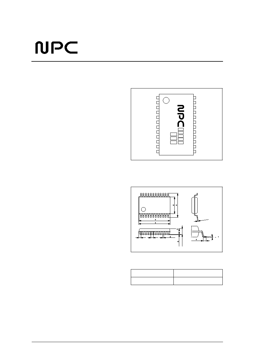
Package
· 24-pin SSOP (SM1350
×××
)
s
Molybdenum-gate CMOS
PINOUT
(TOP VIEW)
PACKAGE DIMENSIONS
24-pin SSOP (Unit: mm)
ORDERING INFOMATION
3
3
3
3
D evice
Packag e
SM1350
×××
M
24pin SSOP
VDD
S0
S1
S2
S3
MODE
LH
XT
XTN
TO
T3N
T2N
T1N
MSBN
SM
1
35
0
STOP
MSB
STN
BUSYN
CT
SP
SPN
VOL
ICN
VSS
1
12
13
24
0.7
0.8
0.36 0.10
10.20 0.30
10.05 0.20
0.10 0.10
2.10MAX
1.80 0.10
7.80 0.30
5.40 0.20
0.15
+
0.1
-
0.05
0 10
0.50 0.20
SM1350 series
NIPPON PRECISION CIRCUITS--2
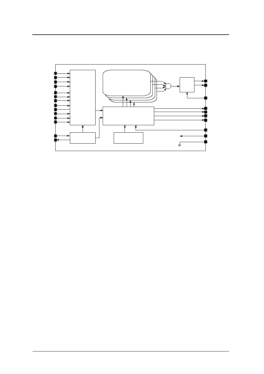
BLOCK DIAGRAM
Arithmetic block Circuit
Control Circuit
Wave ROM
Parameter ROM
Input Circuit
Score ROM
DAC
Oscillator
SP
SPN
VOL
MSB
MSBN
BUSYN
CT
S3
S2
S1
S0
MODE
LH
STOP
STN
TO
T1N
T2N
T3N
XT
XTN
+
ICN
VDD
VSS
SM1350 series
NIPPON PRECISION CIRCUITS--3
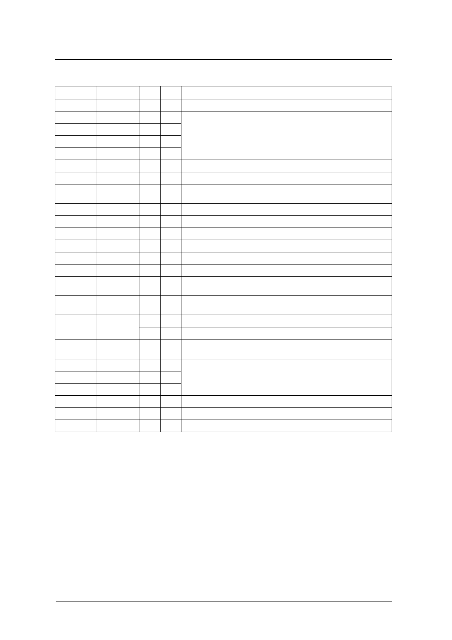
PIN DESCRIPTION
N u m b e r
N a m e
I/O
State
1
1. U = pull-up resistor connection, SU : pull-up resistor connection only when melody output starts,
P = p-channel open drain, C = complementary output.
U or O = pull-up resistance or open drain (master slice)
Description
2
2. BTL/A-class output mode is selected by mask option.
1
VDD
Supply pin
2
S0
I
SU
Binary select mode: Phrase select pins.
Serial select mode: S0 and S1 control melody output.
3
S1
I
SU
4
S2
I
SU
5
S3
I
SU
6
MODE
I
SU
Melody select mode control. Binary mode when LOW, and serial mode when HIGH.
7
LH
I
SU
Melody output mode control. One-shot when LOW, and level hold when HIGH.
8
STOP
I
U or O
One-shot melody mode: Melody output stop control.
Level hold melody mode: Invalid input.
9
STN
I
U or O
Melody start control
10
BUSYN
O
C
Busy output signal. LOW when a melody is output.
11
CT
O
C
External control pulse output
12
ICN
I
U
Initialization clear input
13
VSS
Ground pin
14
VOL
I
Volume adjust control. Volume adjusted using an external resistor.
15
SPN
O
P
9-bit D/A converter output in BTL output mode.
VOL current output in A-class output mode.
16
SP
O
P
BTL output mode: 9-bit D/A converter output.
A-class output mode: 10-bit D/A converter output.
17
MSB
O
C
BTL output mode: Signed-bit output. HIGH when no melody is output.
I
U
A-class output mode: BUSYIN input
18
MSBN
O
C
BTL output mode: Signed-bit output. HIGH when no melody is output.
A-class output mode: ENDN output. HIGH when no melody is output.
19
T1N
I
U
Test signal inputs
20
T2N
I
U
21
T3N
I
U
22
TO
O
C
Test signal output. 62.5 kHz output when not in test mode.
23
XTN
O
Oscillator output
24
XT
I
Oscillator input
SM1350 series
NIPPON PRECISION CIRCUITS--4
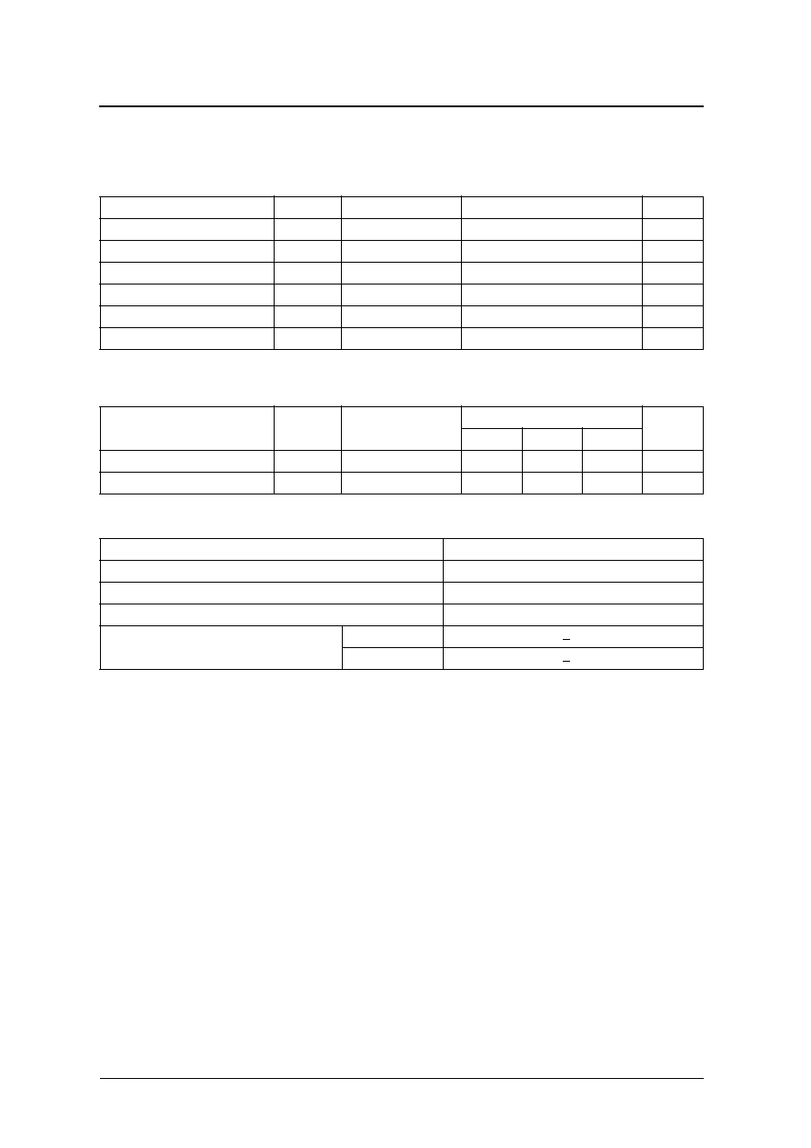
SPECIFICATIONS
Absolute Maximum Ratings
V
SS
= 0 V
Recommended Operating Conditions
V
SS
= 0 V
Master slice
Underlined entries are the default standard options. Throughout this datasheet, the standard options are
assumed unless otherwise specified.
U: pull-up resistance O: open input
P arameter
S y m b o l
Condition
Rating
Unit
Supply voltage
V
DD
-
0.3 to 7.0
V
Input voltage
V
IN
V
SS
-
0.3 to V
DD
+ 0.3
V
Storage temperature
T
stg
-
40 to 125
°
C
Power dissipation
P
D
650
mW
Soldering temperature
T
sld
255
°
C
Soldering time
t
sld
10
s
P arameter
S y m b o l
Condition
Rating
Unit
m i n
typ
m a x
Supply voltage
V
DD
2.4
5.5
V
Operating temperature
T
opr
-
20
80
°
C
S p e c i fi cations
Function Selected condition
Serial-mode melody selections
1 to 16
Melody output circuit
BTL / A-class
Level-hold melody select change retrigger
Yes / No
Pull-up/pull-down resistance
STN
U / O
STOP
U / O
SM1350 series
NIPPON PRECISION CIRCUITS--5
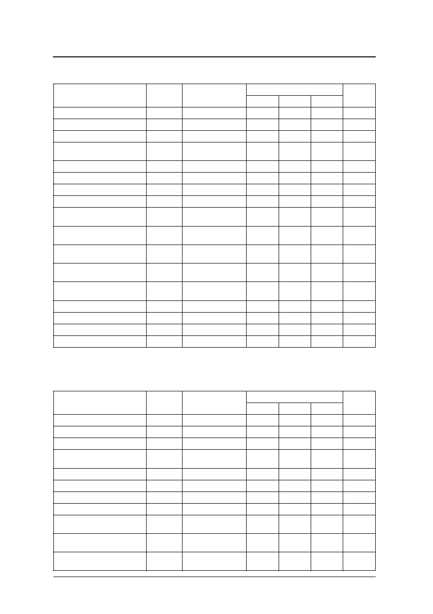
DC Characteristics
V
DD
= 3 V, T
a
= 25
°
C, V
SS
= 0 V, f
O
= 4.0 MHz
1.Supply voltage ratings shown are with oscillator running and all functions operating normally.
2.Clock frequency and duty cycle are ratings for the clock input on pin XT.
3.Output current when 20 k
volume control resistor is connected to VOL, and all D/A converter bits ON, measured using the circuit of the next page.
V
DD
= 5 V, T
a
= 25
°
C, V
SS
= 0 V, f
O
= 4.0 MHz
P arameter
S y m b o l
Condition
Rating
Unit
m i n
typ
m a x
Minimum operating supply voltage
1
V
MIN
2.4
V
Maximum operating supply voltage
1
V
MAX
5.5
V
Standby current consumption
I
STBY
No melody output
1.0
µA
Operating current consumption
I
DD
BUSYN, CT, TO, SP, SPN,
MSB, MSBN all open
3.5
mA
XT external capacitance
C
G
30
pF
XTN external capacitance
C
D
30
pF
Clock frequency
2
f
XTI
3.8
4.0
4.2
MHz
Clock duty cycle
2
R
XTI
40
50
60
%
S0 to S3, MODE, LH, STOP, STN, ICN
HIGH-level input voltage
V
IH
V
DD
-
0.3
V
DD
V
S0 to S3, MODE, LH, STOP, STN, ICN
LOW-level input voltage
V
IL
V
SS
V
SS
+ 0.3
V
S0 to S3, MODE, LH, STOP, STN, ICN
HIGH-level input current
I
IH
V
IH
= V
DD
10
20
µA
S0 to S3, MODE, LH, STOP, STN, ICN
LOW-level input current
I
IL
V
IL
= V
SS
10
20
µA
BUSYN, CT, TO HIGH-level output
current
I
OH1
V
OH1
= V
DD
-
0.7
2.0
mA
BUSYN, CT, TO LOW-level output current
I
OL1
V
OL1
= V
SS
+ 0.7
2.0
mA
MSB, MSBN HIGH-level output current
I
OH2
V
OH2
= V
DD
-
0.7
3.0
mA
MSB, MSBN LOW-level output current
I
OL2
V
OL2
= V
SS
+ 0.7
3.0
mA
SP, SPN output current
3
I
OH3
V
OH3
= V
SS
+ 0.7
4.0
mA
P arameter
S y m b o l
Condition
Rating
Unit
m i n
typ
m a x
Minimum operating supply voltage
1
V
MIN
2.4
V
Maximum operating supply voltage
1
V
MAX
5.5
V
Standby current consumption
I
STBY
No melody output
1.0
µA
Operating current consumption
I
DD
BUSYN, CT, TO, SP, SPN,
MSB, MSBN all open
9.5
mA
XT external capacitance
C
G
30
pF
XTN external capacitance
C
D
30
pF
Clock frequency
2
f
XTI
3.8
4.0
4.2
MHz
Clock duty cycle
2
R
XTI
40
50
60
%
S0 to S3, MODE, LH, STOP, STN, ICN
HIGH-level input voltage
V
IH
V
DD
-
0.3
V
DD
V
S0 to S3, MODE, LH, STOP, STN, ICN
LOW-level input voltage
V
IL
V
SS
V
SS
+ 0.3
V
S0 to S3, MODE, LH, STOP, STN, ICN
HIGH-level input current
I
IH
V
IH
= V
DD
30
50
µA