 | –≠–ª–µ–∫—Ç—Ä–æ–Ω–Ω—ã–π –∫–æ–º–ø–æ–Ω–µ–Ω—Ç: 100329FC | –°–∫–∞—á–∞—Ç—å:  PDF PDF  ZIP ZIP |
100329
Low Power Octal ECL/TTL Bidirectional Translator with
Register
General Description
The 100329 is an octal registered bidirectional translator
designed to convert TTL logic levels to 100K ECL logic levels
and vice versa. The direction of the translation is determined
by the DIR input. A LOW on the output enable input (OE)
holds the ECL outputs in a cut-off state and the TTL outputs
at
a
high
impedance
level.
The
outputs
change
synchronously with the rising edge of the clock input (CP)
even though only one output is enabled at the time.
The cut-off state is designed to be more negative than a
normal
ECL
LOW
level.
This
allows
the
output
emitter-followers to turn off when the termination supply is
-2.0V, presenting a high impedance to the data bus. This
high impedance reduces the termination power and prevents
loss of low state noise margin when several loads share the
bus.
The 100329 is designed with FAST
Æ
TTL output buffers,
featuring optimal DC drive and capable of quickly charging
and discharging highly capacitive loads. All inputs have
50 k
pull-down resistors.
Features
n
Bidirectional translation
n
ECL high impedance outputs
n
Registered outputs
n
FAST TTL outputs
n
TRI-STATE
Æ
outputs
n
Voltage compensated operating range = -4.2V to -5.7V
n
Standard Microcircuit Drawing
(SMD) 5962-9206601
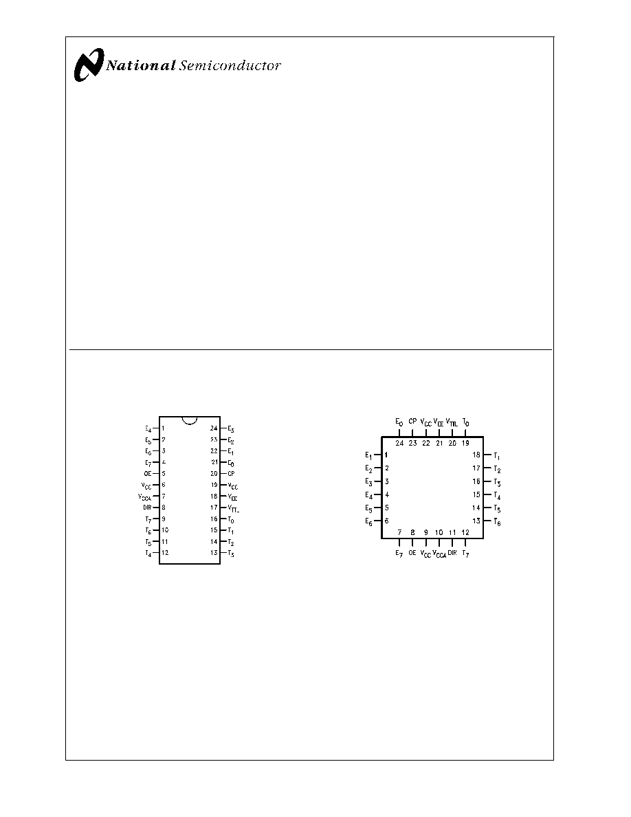
Connection Diagrams
TRI-STATE
Æ
is a registered trademark of National Semiconductor Corporation.
FAST
Æ
is a registered trademark of Fairchild Semiconductor.
24-Pin DIP
DS100306-2
24-Pin Quad Cerpack
DS100306-4
September 1999
100329
Low
Power
Octal
ECL/TTL
Bidirectional
T
ranslator
with
Register
© 2001 National Semiconductor Corporation
DS100306
www.national.com

Logic Symbol
Pin Descriptions
Pin Names
Description
E
0
≠E
7
ECL Data I/O
T
0
≠T
7
TTL Data I/O
OE
Output Enable Input
CP
Clock Pulse Input
(Active Rising Edge)
DIR
Direction Control Input
All pins function at 100K ECL levels except for T
0
≠T
7
.
Functional Diagram
DS100306-1
DS100306-5
Note: DIR and OE use ECL logic levels
100329
www.national.com
2
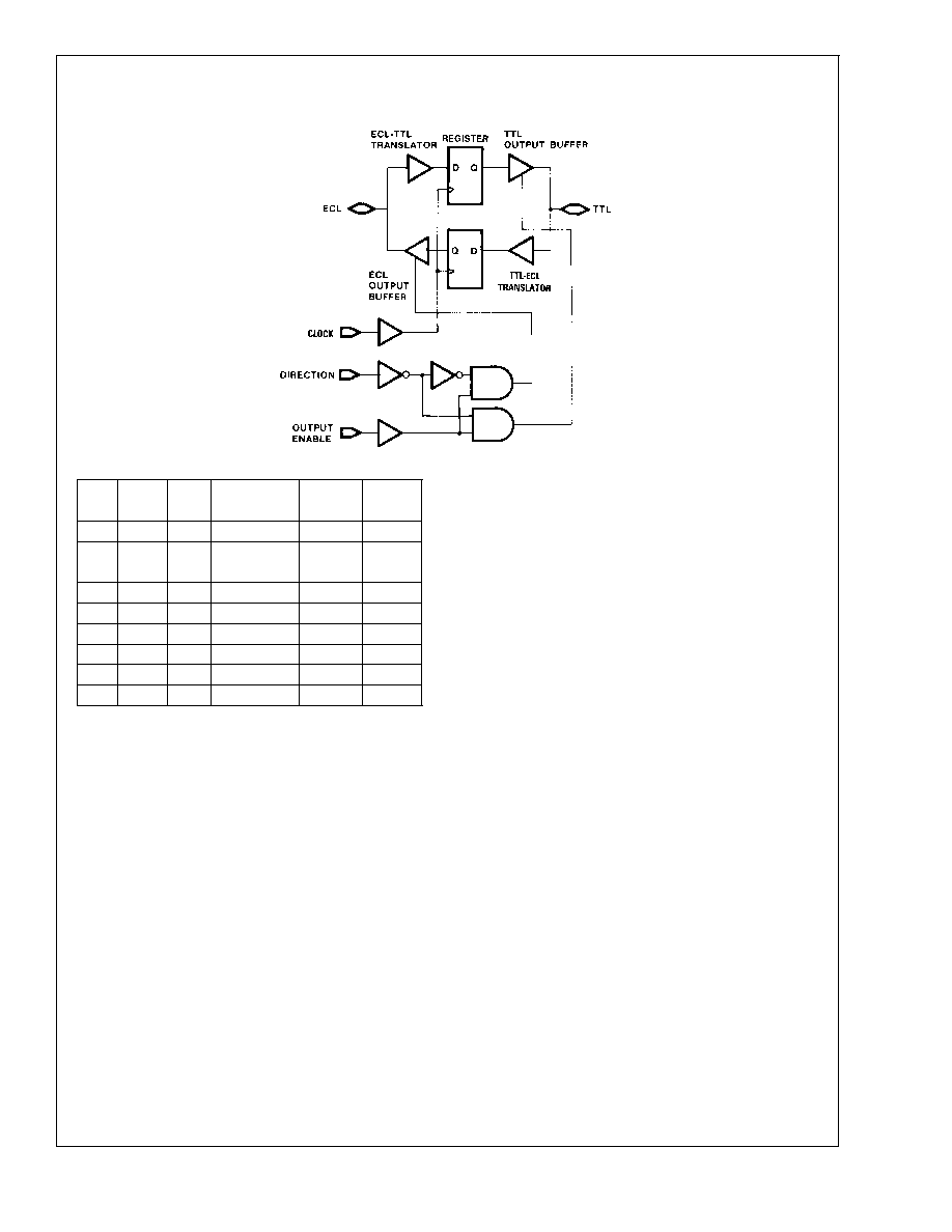
Detail
OE
DIR
CP
ECL
TTL
Notes
Port
Port
L
L
X
Input
Z
1, 3
L
H
X
LOW
Input
2, 3
(Cut-Off)
H
L
N
L
L
1
H
L
N
H
H
1
H
L
L
X
NC
1, 3
H
H
N
L
L
2
H
H
N
H
H
2
H
H
L
NC
X
2, 3
H = HIGH Voltage Level
L = LOW Voltage Level
X = Don't Care
Z = High Impedance
N
= LOW-to-HIGH Clock Transition
NC = No Change
Note 1: ECL input to TTL output mode.
Note 2: TTL input to ECL output mode.
Note 3: Retains data present before CP.
DS100306-6
100329
www.national.com
3

Absolute Maximum Ratings
(Note 4)
If Military/Aerospace specified devices are required,
please contact the National Semiconductor Sales
Office/Distributors for availability and specifications.
Storage Temperature (T
STG
)
-65∞C to +150∞C
Maximum Junction Temperature (T
j
)
Ceramic
+175∞C
V
EE
Pin Potential to
Ground Pin
-7.0V to +0.5V
V
TTL
Pin Potential to
Ground Pin
-0.5V to +6.0V
ECL Input Voltage (DC)
V
EE
to +0.5V
ECL Output Current
(DC Output HIGH)
-50 mA
TTL Input Voltage (Note 6)
-0.5V to +6.0V
TTL Input Current (Note 6)
-30 mA to +5.0 mA
Voltage Applied to Output in HIGH State
TRI-STATE Output
-0.5V to +5.5V
Current Applied to TTL
Output in LOW State (Max)
Twice the Rated I
OL
(mA)
ESD (Note 5)
2000V
Recommended Operating
Conditions
Case Temperature (T
C
)
Military
≠55∞C to +125∞C
ECL Supply Voltage (V
EE
)
-5.7V to -4.2V
TTL Supply Voltage (V
TTL
)
+4.5V to +5.5V
Note 4: Absolute maximum ratings are those values beyond which the
device may be damaged or have its useful life impaired. Functional operation
under these conditions is not implied.
Note 5: ESD testing conforms to MIL-STD-883, Method 3015.
Note 6: Either voltage limit or current limit is sufficient to protect inputs.
Military Version
TTL-to-ECL DC Electrical Characteristics
V
EE
= -4.2V to -5.7V, V
CC
= V
CCA
= GND, T
C
= -55∞C to +125∞C, V
TTL
= +4.5V to +5.5V
Symbol
Parameter
Min
Max
Units
T
C
Conditions
Notes
V
OH
Output HIGH Voltage
-1025
-870
mV
0∞C to
Loading with
50
to -2.0V
(Notes 7, 8,
9)
+125∞C
-1085
-870
mV
-55∞C
V
IN
= V
IH
(Max)
V
OL
Output LOW Voltage
-1830
-1620
mV
0∞C to
or V
IL
(Min)
+125∞C
-1830
-1555
mV
-55∞C
Cutoff Voltage
-1950
mV
0∞C to
+125∞C
OE or DIR Low
-1850
mV
-55∞C
V
OHC
Output HIGH Voltage
-1035
mV
0∞C to
(Notes 7, 8,
9)
+125∞C
-1085
mV
-55∞C
V
IN
= V
IH
(Min)
Loading with
V
OLC
Output LOW Voltage
-1610
mV
0∞C to
or V
IL
(Max)
50
0 to -2.0V
+125∞C
-1555
mV
-55∞C
V
IH
Input HIGH Voltage
2.0
V
-55∞C to
Over V
TTL
, V
EE
, T
C
Range
(Notes 7, 8,
9, 10)
+125∞C
V
IL
Input LOW Voltage
0.8
V
-55∞C to
Over V
TTL
, V
EE
, T
C
Range
(Notes 7, 8,
9, 10)
+125∞C
I
IH
Input HIGH Current
70
µA
-55∞C to
V
IN
= +2.7V
(Notes 7, 8,
9)
125∞C
Breakdown Test
1.0
mA
-55∞C to
V
IN
= +5.5V
+125∞C
I
IL
Input LOW Current
-1.0
mA
-55∞C to
V
IN
= +0.5V
(Notes 7, 8,
9)
+125∞C
V
FCD
Input Clamp
-1.2
V
-55∞C to
I
IN
= -18 mA
(Notes 7, 8,
9)
Diode Voltage
+125∞ C
I
EE
V
EE
Supply Current
-55∞C to
OE and DIR High
(Notes 7, 8,
9)
Inputs Open
-206
-70
mA
+125∞C
V
EE
= -4.2V to -5.7V
100329
www.national.com
4

Military Version
ECL-to-TTL DC Electrical Characteristics
V
EE
= -4.2V to -5.7V, V
CC
= V
CCA
= GND, T
C
= -55∞C to +125∞C, C
L
= 50 pF, V
TTL
= +4.5V to + 5.5V
Symbol
Parameter
Min
Max Units
T
C
Conditions
Notes
V
OH
Output HIGH Voltage
2.5
mV
0∞C to +125∞C
I
OH
= -1 mA, V
TTL
= 4.50V
(Notes 7, 8, 9)
2.4
-55∞C
V
OL
Output LOW Voltage
0.5
mV
-55∞C
I
OL
= 24 mA, V
TTL
= 4.50V
+125∞C
V
IH
Input HIGH Voltage
-1165
-870
mV
-55∞C
Guaranteed HIGH Signal
(Notes 7, 8, 9, 10)
+125∞C
for All Inputs
V
IL
Input LOW Voltage
-1830 -1475
mV
-55∞C to
Guaranteed LOW Signal
(Notes 7, 8, 9, 10)
+125∞C
for All Inputs
I
IH
Input HIGH Current
350
µA
0∞C to
V
EE
= -5.7V
(Notes 7, 8, 9)
500
+125∞C
V
IN
= V
IH
(Max)
I
IL
Input LOW Current
0.50
µA
-55∞C to
V
EE
= -4.2V
(Notes 7, 8, 9)
+125∞C
V
IN
= V
IL
(Min)
I
OZHT
TRI-STATE Current
70
µA
-55∞C to
V
OUT
= +2.7V
(Notes 7, 8, 9)
Output High
+125∞C
I
OZLT
TRI-STATE Current
-1.0
mA
-55∞C to
V
OUT
= +0.5V
(Notes 7, 8, 9)
Output Low
+125∞C
I
OS
Output Short-Circuit
-60
-150
mA
-55∞C to
V
OUT
= 0.0V, V
TTL
= +5.5V
(Notes 7, 8, 9)
CURRENT
+125∞C
I
TTL
V
TTL
Supply Current
70
mA
-55∞C to
TTL Outputs Low
(Notes 7, 8, 9)
47
mA
+125∞C
TTL Output High
70
mA
TTL Output in TRI-STATE
Note 7: F100K 300 Series cold temperature testing is performed by temperature soaking (to guarantee junction temperature equals -55∞C), then testing
immediately without allowing for the junction temperature to stabilize due to heat dissipation after power-up. This provides "cold start" specs which can be considered
a worst case condition at cold temperatures.
Note 8: Screen tested 100% on each device at -55∞C, +25∞C, and +125∞C, Subgroups, 1, 2 3, 7, and 8.
Note 9: Sample tested (Method 5005, Table I) on each manufactured lot at -55∞C, +25∞C, and +125∞C, Subgroups A1, 2, 3, 7, and 8.
Note 10: Guaranteed by applying specified input condition and testing V
OH
/V
OL
.
Military Version
TTL-to-ECL AC Electrical Characteristics
V
EE
= -4.2V to -5.7V, V
TTL
= +4.5V to +5.5V, V
CC
= V
CCA
= GND
Symbol
Parameter
T
C
= -55∞C
T
C
= 25∞C
T
C
=
+125∞C
Units
Conditions
Notes
Min
Max
Min
Max
Min
Max
t
PLH
CP to E
n
1.3
3.8
1.6
3.7
1.9
4.3
ns
Figures 1, 2
(Notes 11,
12, 13)
t
PHL
ns
t
PZH
OE to E
n
1.0
4.3
1.5
4.4
1.7
9.0
ns
Figures 1, 2
(Notes 11,
12, 13)
(Cutoff to HIGH)
t
PHZ
OE to E
n
1.5
5.0
1.6
4.5
1.6
5.0
ns
Figures 1, 2
(HIGH to Cutoff)
t
PHZ
DIR to E
n
1.6
4.7
1.6
4.3
1.7
4.7
ns
Figures 1, 2
(HIGH to Cutoff)
t
set
T
n
to CP
2.5
2.0
2.5
ns
Figures 1, 2
(Note 14)
t
hold
T
n
to CP
2.5
2.0
2.5
ns
Figures 1, 2
t
pw
(H)
Pulse Width CP
2.5
2.0
2.5
ns
Figures 1, 2
(Note 14)
t
TLH
Transition Time
0.4
2.3
0.5
2.1
0.4
2.4
ns
Figures 1, 2
(Note 14)
t
THL
20% to 80%, 80% to 20%
f
MAX
CP
250
250
250
MHz
100329
www.national.com
5