 | –≠–ª–µ–∫—Ç—Ä–æ–Ω–Ω—ã–π –∫–æ–º–ø–æ–Ω–µ–Ω—Ç: 4016BC | –°–∫–∞—á–∞—Ç—å:  PDF PDF  ZIP ZIP |
TL F 5661
CD4016BMCD4016BC
Quad
Bilateral
Switch
August 1989
CD4016BM CD4016BC Quad Bilateral Switch
General Description
The CD4016BM CD4016BC is a quad bilateral switch in-
tended for the transmission or multiplexing of analog or digi-
tal signals It is pin-for-pin compatible with CD4066BM
CD4066BC
Features
Y
Wide supply voltage range
3V to 15V
Y
Wide range of digital and analog switching
g
7 5 V
PEAK
Y
``ON'' resistance for 15V operation
400X (typ )
Y
Matched ``ON'' resistance over 15V
signal input
D
R
ON
e
10X (typ )
Y
High degree of linearity
0 4% distortion (typ )
f
IS
e
1 kHz V
IS
e
5 V
p-p
V
DD
b
V
SS
e
10V R
L
e
10 kX
Y
Extremely low ``OFF'' switch leakage
0 1 nA (typ )
V
DD
b
V
SS
e
10V
T
A
e
25 C
Y
Extremely high control input impedance
10
12
X
(typ )
Y
Low crosstalk between switches
b
50 dB (typ )
f
IS
e
0 9 MHz R
L
e
1 kX
Y
Frequency response switch ``ON''
40 MHz (typ )
Applications
Y
Analog signal switching multiplexing
Signal gating
Squelch control
Chopper
Modulator Demodulator
Commutating switch
Y
Digital signal switching multiplexing
Y
CMOS logic implementation
Y
Analog-to-digital digital-to-analog conversion
Y
Digital control of frequency impedance phase and an-
alog-signal gain
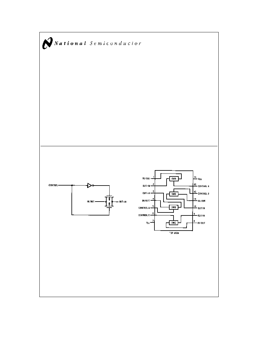
Schematic and Connection Diagrams
Dual-In-Line Package
TL F 5661 ≠ 1
Order Number CD4016B
C1995 National Semiconductor Corporation
RRD-B30M105 Printed in U S A
Absolute Maximum Ratings
If Military Aerospace specified devices are required
please contact the National Semiconductor Sales
Office Distributors for availability and specifications
(Notes 1 and 2)
V
DD
Supply Voltage
b
0 5V to
a
18V
V
IN
Input Voltage
b
0 5V to V
DD
a
0 5V
T
S
Storage Temperature Range
b
65 C to
a
150 C
Power Dissipation (P
D
)
Dual-In-Line
700 mW
Small Outline
500 mW
Lead Temperature (Soldering 10 seconds)
260 C
Recommended Operating
Conditions
(Note 2)
V
DD
Supply Voltage
3V to 15V
V
IN
Input Voltage
0V to V
DD
T
A
Operating Temperature Range
CD4016BM
b
55 C to
a
125 C
CD4016BC
b
40 C to
a
85 C
DC Electrical Characteristics
CD4016BM (Note 2)
Symbol
Parameter
Conditions
b
55 C
25 C
125 C
Units
Min
Max
Min
Typ
Max
Min
Max
I
DD
Quiescent Device Current
V
DD
e
5V V
IN
e
V
DD
or V
SS
0 25
0 01
0 25
7 5
m
A
V
DD
e
10V V
IN
e
V
DD
or V
SS
0 5
0 01
0 5
15
m
A
V
DD
e
15V V
IN
e
V
DD
or V
SS
1 0
0 01
1 0
30
m
A
Signal Inputs and Outputs
R
ON
``ON'' Resistance
R
L
e
10 kX to
V
DD
b
V
SS
2
V
C
e
V
DD
V
IS
e
V
SS
or V
DD
V
DD
e
10V
600
250
660
960
X
V
DD
e
15V
360
200
400
600
X
R
L
e
10 kX to
V
DD
b
V
SS
2
V
C
e
V
DD
V
DD
e
10V V
IS
e
4 75 to 5 25V
1870
850
2000
2600
X
V
DD
e
15V V
IS
e
7 25 to 7 75V
775
400
850
1230
X
D
R
ON
D
``ON'' Resistance
R
L
e
10 kX to
V
DD
b
V
SS
2
Between any 2 of
V
C
e
V
DD
V
IS
e
V
SS
to V
DD
4 Switches
V
DD
e
10V
15
X
(In Same Package)
V
DD
e
15V
10
X
I
IS
Input or Output Leakage
V
C
e
0 V
DD
e
15V
g
50
g
0 1
g
50
g
500
nA
Switch ``OFF''
V
IS
e
15V and 0V
V
OS
e
0V and 15V
Control Inputs
V
ILC
Low Level Input Voltage
V
IS
e
V
SS
and V
DD
V
OS
e
V
DD
and V
SS
I
IS
e
g
10 mA
V
DD
e
5V
0 9
0 7
0 5
V
V
DD
e
10V
0 9
0 7
0 5
V
V
DD
e
15V
0 9
0 7
0 5
V
V
IHC
High Level Input Voltage
V
DD
e
5V
3 5
3 5
3 5
V
V
DD
e
10V
(see Note 6 and
7 0
7 0
7 0
V
V
DD
e
15V
Figure 8 )
11 0
11 0
11 0
V
I
IN
Input Current
V
DD
b
V
SS
e
15V
g
0 1
g
10
b
5
g
0 1
g
1 0
m
A
V
DD
t
V
IS
t
V
SS
V
DD
t
V
C
t
V
SS
2
DC Electrical Characteristics
CD4016BC (Note 2) (Continued)
Symbol
Parameter
Conditions
b
40 C
25 C
85 C
Units
Min
Max
Min
Typ
Max
Min
Max
I
DD
Quiescent Device Current
V
DD
e
5V V
IN
e
V
DD
or V
SS
1 0
0 01
1 0
7 5
m
A
V
DD
e
10V V
IN
e
V
DD
or V
SS
2 0
0 01
2 0
15
m
A
V
DD
e
15V V
IN
e
V
DD
or V
SS
4 0
0 01
4 0
30
m
A
Signal Inputs and Outputs
R
ON
``ON'' Resistance
R
L
e
10 kX to
V
DD
b
V
SS
2
V
C
e
V
DD
V
IS
e
V
SS
or V
DD
V
DD
e
10V
610
275
660
840
X
V
DD
e
15V
370
200
400
520
X
R
L
e
10 kX to
V
DD
b
V
SS
2
V
C
e
V
DD
V
DD
e
10V V
IS
e
4 75 to 5 25V
1900
850
2000
2380
X
V
DD
e
15V V
IS
e
7 25 to 7 75V
790
400
850
1080
X
D
R
ON
D
``ON'' Resistance
R
L
e
10 kX to
V
DD
b
V
SS
2
Between any 2 of
V
C
e
V
DD
V
IS
e
V
SS
to V
DD
4 Switches
V
DD
e
10V
15
X
(In Same Package)
V
DD
e
15V
10
X
I
IS
Input or Output Leakage
V
C
e
0 V
DD
e
15V
g
50
g
0 1
g
50
g
200
nA
Switch ``OFF''
V
IS
e
0V or 15V
V
OS
e
15V or 0V
Control Inputs
V
ILC
Low Level Input Voltage
V
IS
e
V
SS
and V
DD
V
OS
e
V
DD
and V
SS
I
IS
e
g
10 mA
V
DD
e
5V
0 9
0 7
0 4
V
V
DD
e
10V
0 9
0 7
0 4
V
V
DD
e
15V
0 9
0 7
0 4
V
V
IHC
High Level Input Voltage
V
DD
e
5V
3 5
3 5
3 5
V
V
DD
e
10V
(see Note 6 and
7 0
7 0
7 0
V
V
DD
e
15V
Figure 8 )
11 0
11 0
11 0
V
I
IN
Input Current
V
CC
b
V
SS
e
15V
g
0 3
g
10
b
5
g
0 3
g
1 0
m
A
V
DD
t
V
IS
t
V
SS
V
DD
t
V
C
t
V
SS
AC Electrical Characteristics
T
A
e
25 C t
r
e
t
f
e
20 ns and V
SS
e
0V unless otherwise specified
Symbol
Parameter
Conditions
Min
Typ
Max
Units
t
PHL
t
PLH
Propagation Delay Time
V
C
e
V
DD
C
L
e
50 pF (
Figure 1 )
Signal Input to Signal Output
R
L
e
200k
V
DD
e
5V
58
100
ns
V
DD
e
10V
27
50
ns
V
DD
e
15V
20
40
ns
t
PZH
t
PZL
Propagation Delay Time
R
L
e
1 0 kX C
L
e
50 pF (
Figures 2
Control Input to Signal
and
3 )
Output High Impedance to
V
DD
e
5V
20
50
ns
Logical Level
V
DD
e
10V
18
40
ns
V
DD
e
15V
17
35
ns
t
PHZ
t
PLZ
Propagation Delay Time
R
L
e
1 0 kX C
L
e
50 pF (
Figures 2
Control Input to Signal
and
3 )
Output Logical Level to
V
DD
e
5V
15
40
ns
High Impedance
V
DD
e
10V
11
25
ns
V
DD
e
15V
10
22
ns
Sine Wave Distortion
V
C
e
V
DD
e
5V V
SS
e b
5
0 4
%
R
L
e
10 kX V
IS
e
5 V
P-P
f
e
1 kHz
(
Figure 4 )
3
AC Electrical Characteristics
(Continued)
T
A
e
25 C t
r
e
t
f
e
20 ns and V
SS
e
0V unless otherwise specified
Symbol
Parameter
Conditions
Min
Typ
Max
Units
Frequency Response
Switch
V
C
e
V
DD
e
5V V
SS
e b
5V
40
MHz
``ON'' (Frequency at
b
3 dB)
R
L
e
1 kX V
IS
e
5 V
P-P
20 Log
10
V
OS
V
OS
(1 kHz)
b
dB
(
Figure 4 )
Feedthrough
Switch ``OFF''
V
DD
e
5V V
C
e
V
SS
e b
5V
1 25
MHz
(Frequency at
b
50 dB)
R
L
e
1 kX V
IS
e
5 V
P-P
20 Log
10
(V
OS
V
IS
)
e b
50 dB
(
Figure 4 )
Crosstalk Between Any Two
V
DD
e
V
C(A)
e
5V V
SS
e
V
C(B)
e b
5V
0 9
MHz
Switches (Frequency at
b
50 dB)
R
L
e
1 kXV
IS(A)
e
5 V
P-P
20 Log
10
(V
OS(B)
V
OS(A)
)
e b
50 dB
(
Figure 5 )
Crosstalk Control Input to
V
DD
e
10V R
L
e
10 kX
150
mV
P-P
Signal Output
R
IN
e
1 kX V
CC
e
10V Square Wave
C
L
e
50 pF (
Figure 6 )
Maximum Control Input
R
L
e
1 kX C
L
e
50 pF (
Figure 7 )
V
OS(f)
e
V
OS
(1 kHz)
V
DD
e
5V
6 5
MHz
V
DD
e
10V
8 0
MHz
V
DD
e
15V
9 0
MHz
C
IS
Signal Input Capacitance
4
pF
C
OS
Signal Output Capacitance
V
DD
e
10V
4
pF
C
IOS
Feedthrough Capacitance
V
C
e
0V
0 2
pF
C
IN
Control Input Capacitance
5
7 5
pF
AC Paramters are guaranteed by DC correlated testing
Note 1
``Absolute Maximum Ratings'' are those values beyond which the safety of the device cannot be guaranteed They are not meant to imply that the devices
should be operated at these limits The tables of ``Recommended Operating Conditions'' and ``Electrical Characteristics'' provide conditions for actual device
operation
Note 2
V
SS
e
0V unless otherwise specified
Note 3
These devices should not be connected to circuits with the power ``ON''
Note 4
In all cases there is approximately 5 pF of probe and jig capacitance on the output however this capacitance is included in C
L
wherever it is specified
Note 5
V
IS
is the voltage at the in out pin and V
OS
is the voltage at the out in pin V
C
is the voltage at the control input
Note 6
If the switch input is held at V
DD
V
IHC
is the control input level that will cause the switch output to meet the standard ``B'' series V
OH
and I
OH
output levels
If the analog switch input is connected to V
SS
V
IHC
is the control input level
which allows the switch to
sink standard ``B'' series
l
I
OH
l
high level current and still
maintain a V
OL
s
``B'' series These currents are shown in
Figure 8
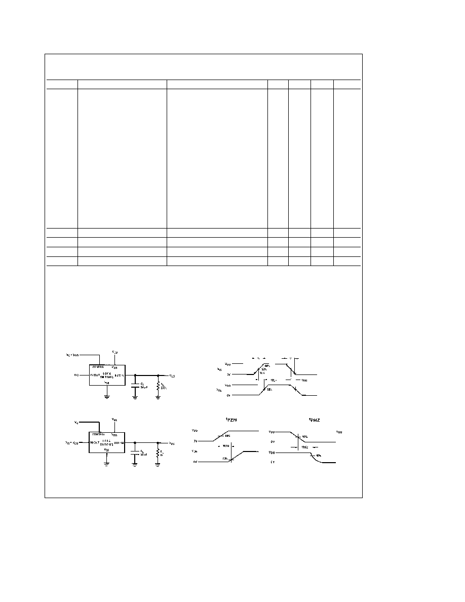
AC Test Circuits and Switching Time Waveforms
Figure 1 t
PLH
t
PLH
Propagation Delay Time Signal Input to Signal Output
TL F 5661 ≠ 2
FIGURE 2 t
PZH
t
PHZ
Propagation Delay Time Control to Signal Output
4

AC Test Circuits and Switching Time Waveforms
(Continued)
FIGURE 3 t
PZH
t
PHZ
Propagation Delay Time Control to Signal Output
V
C
e
V
DD
for distortion and frequency response tests
V
C
e
V
SS
for feedthrough test
FIGURE 4 Sine Wave Distortion Frequency Response and Feedthrough
FIGURE 5 Crosstalk Between Any Two Switches
TL F 5661 ≠ 3
FIGURE 6 Crosstalk
Control to Input Signal Output
5